Learning Eagle from tutorials
At the end of may and beginning of june 2023, I decided to follow some webinars about Eagle. The Autodesk EAGLE team is represented by: Edwin Robledo and Jorge Garcia. The goal is to make a personal documentation, kind of help manual, a reminder, I will know exactly where I have to pick my information.
The webinar is here and there are two parts. Part one is about the control panel and the schematics. Part two is about designing board, manufacturing.
To be quick in the documentation, I will use these shorcuts:
| shorcuts | definition |
|---|---|
| LMB | Left Mouse Button |
| MMB | Middle Mouse Button |
| RMB | Right Mouse Button |
This is my personal documentation, if you need more information, go to the MIT help
Control panel:
You open the software you will face the control panel. It is full of different stuffs important to activate before.
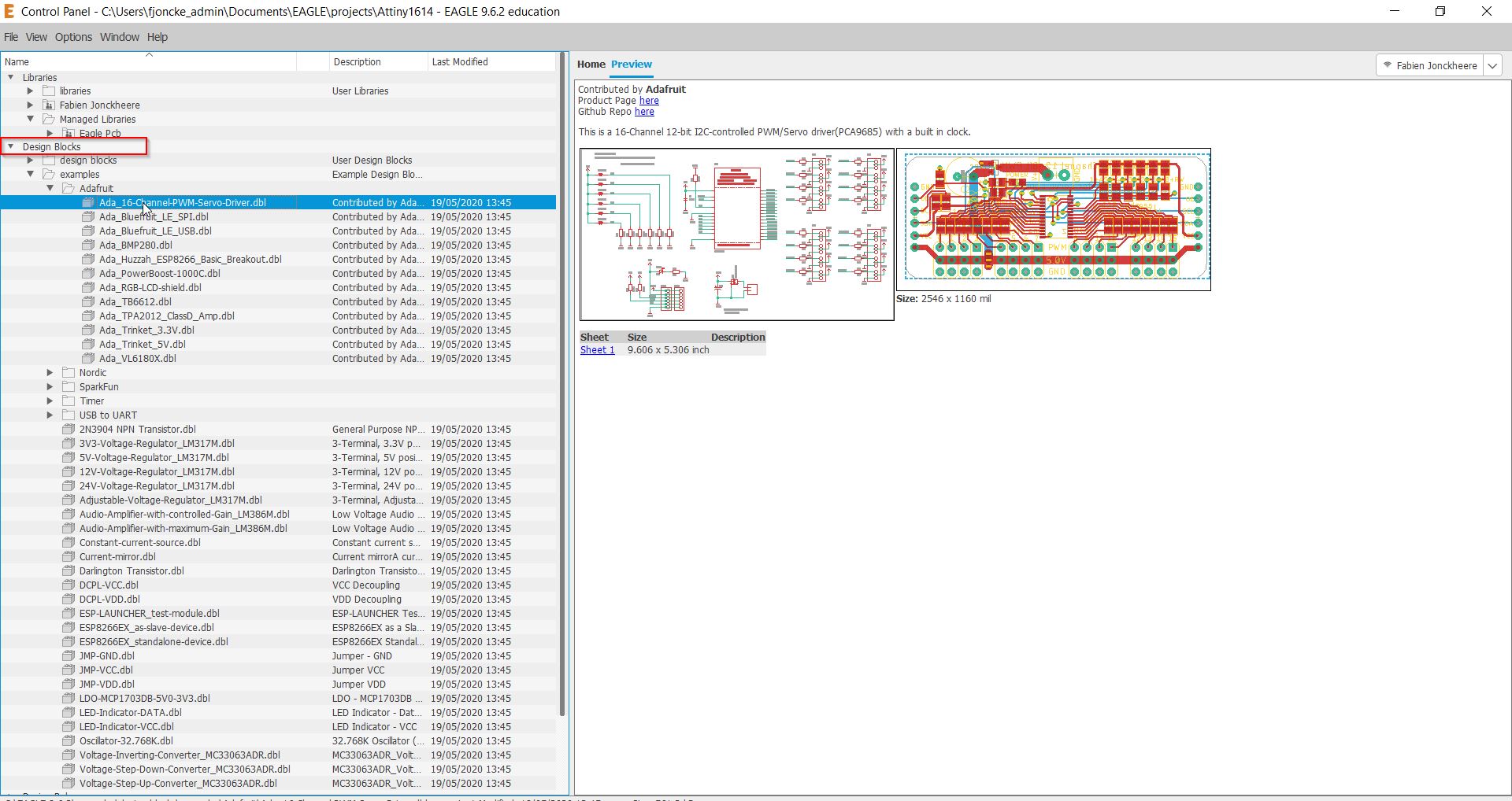
- Libraries:
There are the libraries organized by local, cloud datas.
The folder called Fabien Jonckheere is my local computer library.

- Design blocks
You have the design blocks. Electronics brands such as adafruit, sparkfun have created a lot of electronics blocks ready to add on your projects. You also can create your own design blocks.
- Design rules check
Design Rules define all the parameters that the board layout has to follow. (thickness of routing path, etc…)
- User language Programs.
Not seen yet.
- Scripts
Not seen yet.
- CAM Jobs
Not seen yet.
- Spice models.
From and more info on ROHMS
SPICE is open-source software that simulates the operating conditions of analog circuits. It is short for ‘Simulation Program with Integrated Circuit Emphasis’.
More specifically, it is a general-purpose circuit simulation program that provides linear AC analysis, non-linear transient analysis, and nonlinear DC analysis.
Analysis is performed by solving combinations of theoretical and experimental (device model) equations representing the behavior of elements based on Kirkhoff’s current and voltage laws, utilizing modified nodal point analysis.
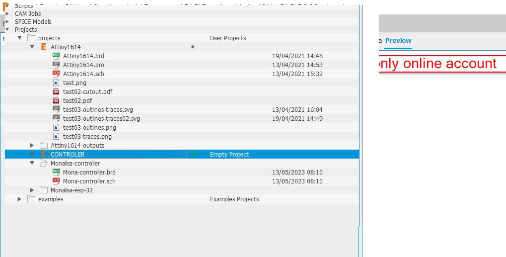
- Projects All your projects including Schematics and boards.
Availibility
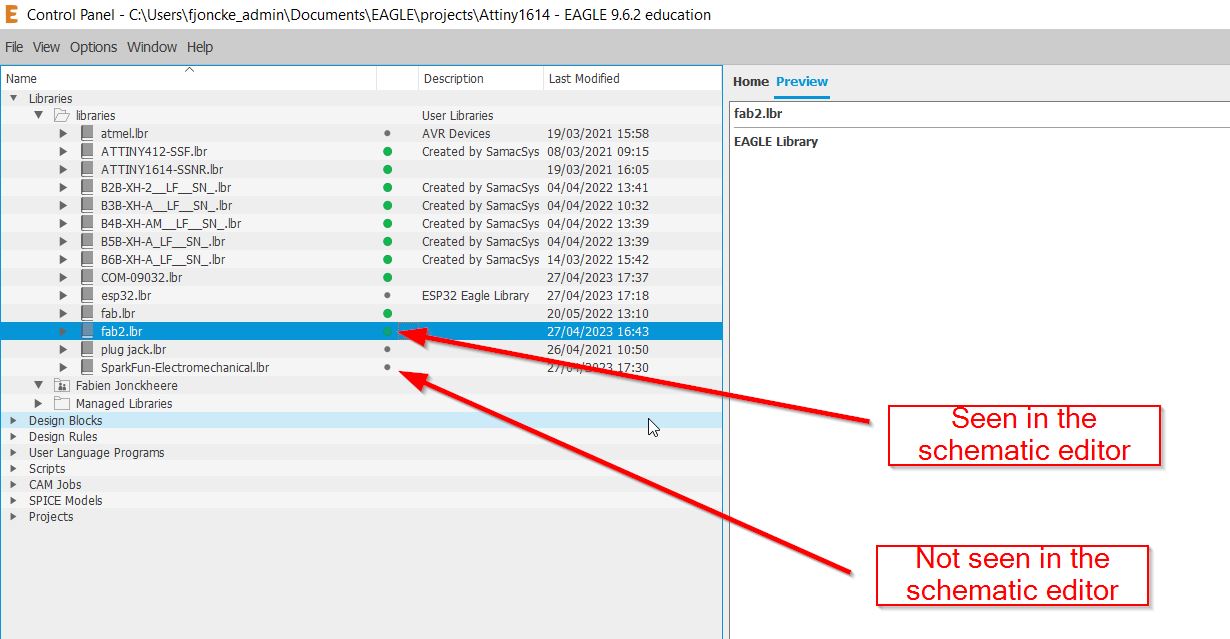
It is easy to get messy if you have everything available, that is why the green light show the availibility or not when you will work on your schematic.
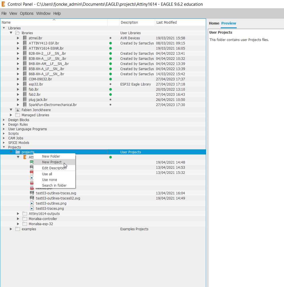
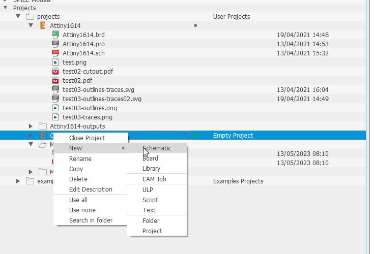
New project
Go to project, and [RMB] to create a new project.
 ///////check this pix///////
New Schematic.
[RMB] and create a new schematic.
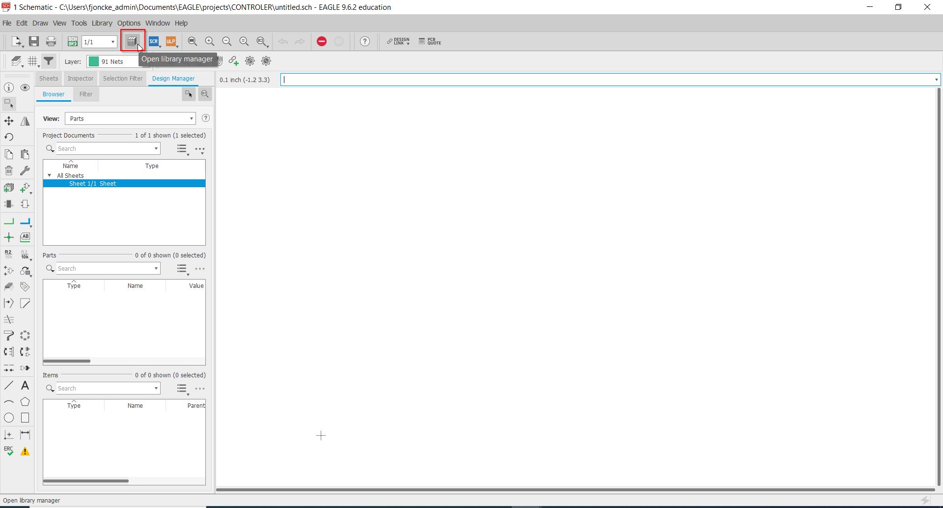
Schematic design
available libraries
On the schematic panel, you will also have the editor of the libraries. And you can see the libraries highlighted in green in the control panel.
add parts
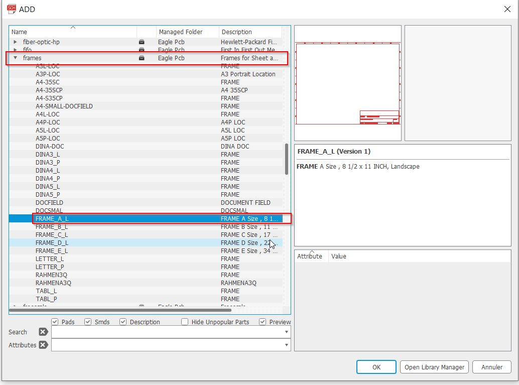
Frame
First at all, you need to get a frame to your schematic. You need to click on “add part”.
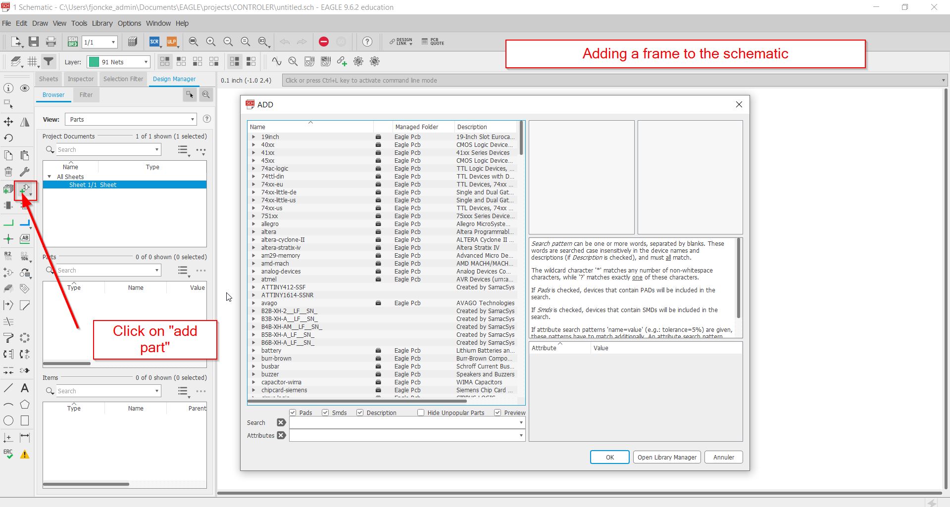
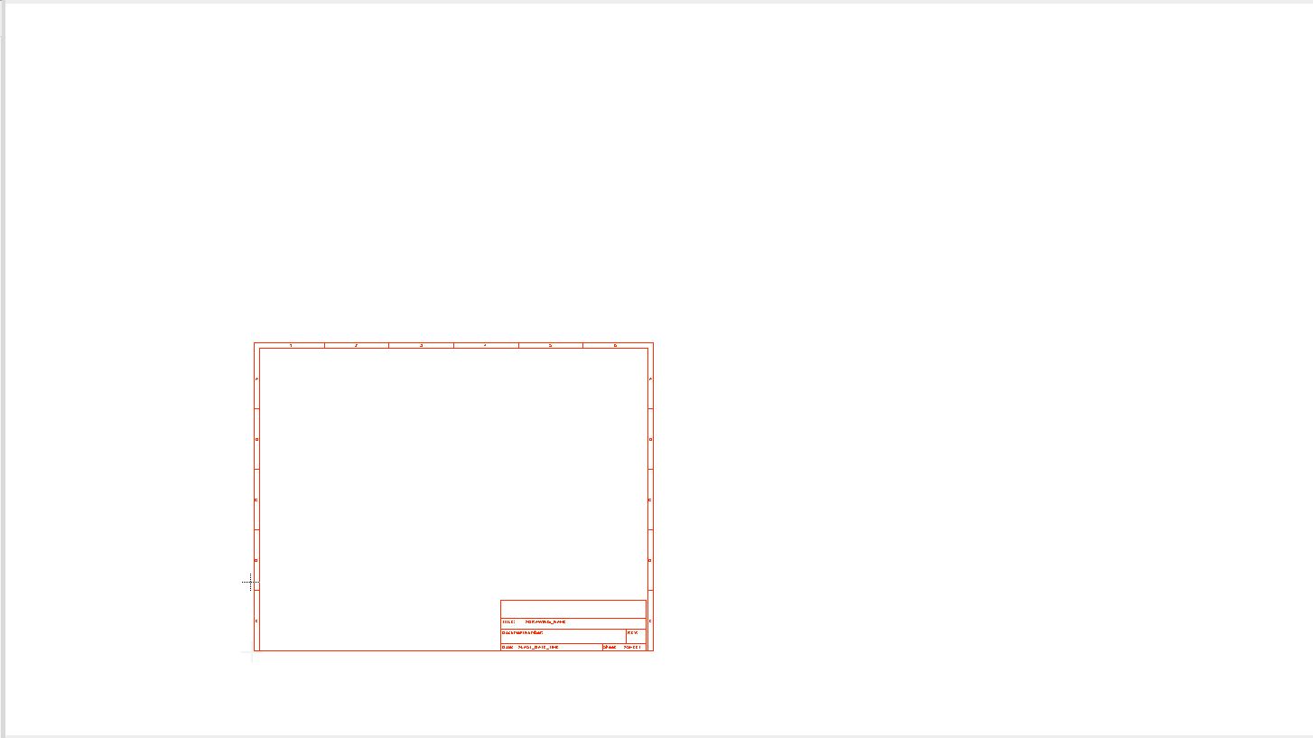
Select the frame you want:
You can easily zoom by [MMB].
 Check the origins 0.0 to install your frame. Always work on the positive side (Look at the bright side of life dixit Monty Python)
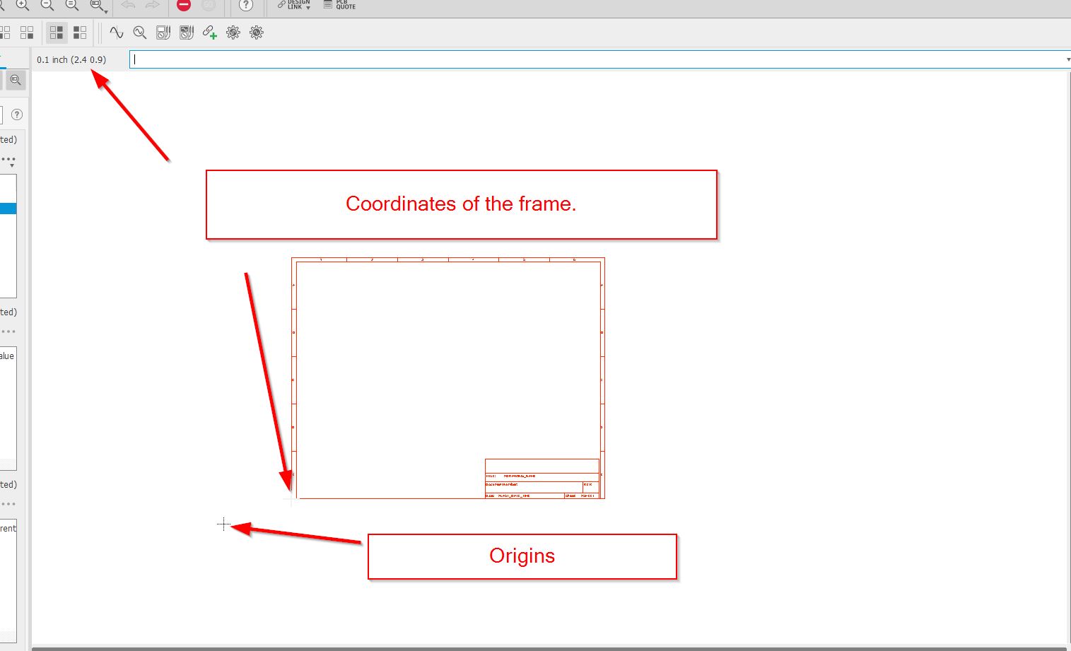
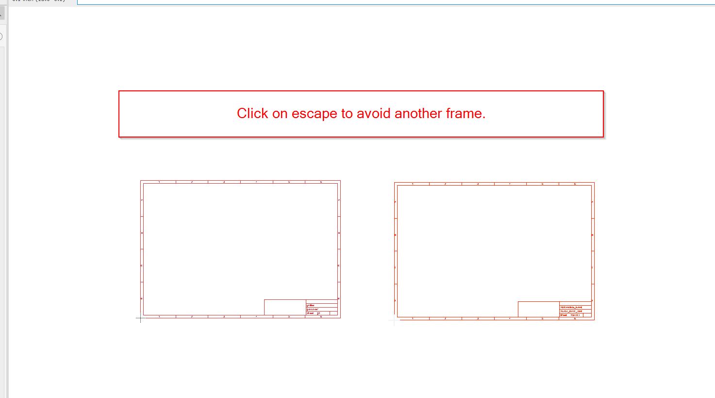
Escape.
components
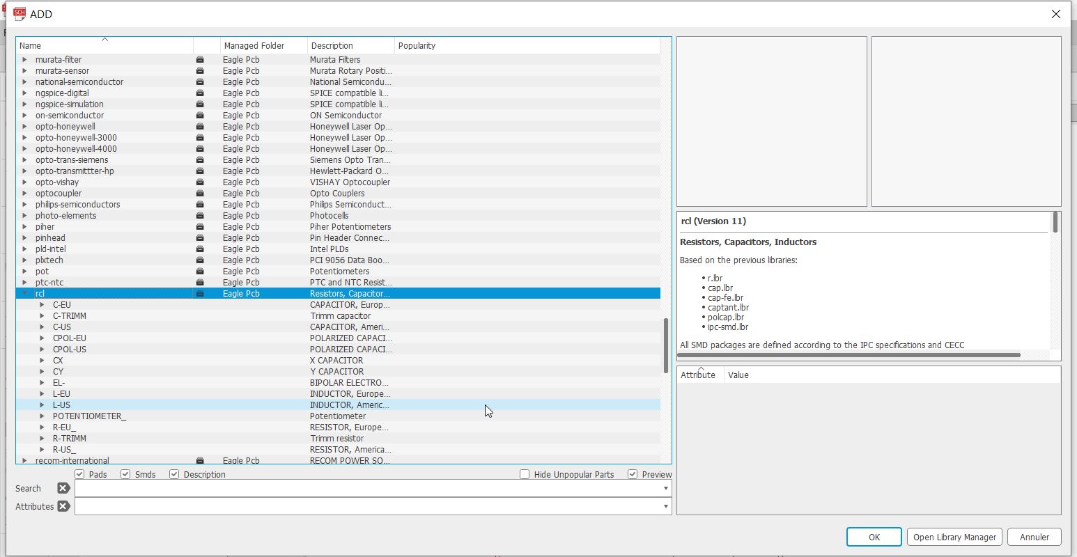
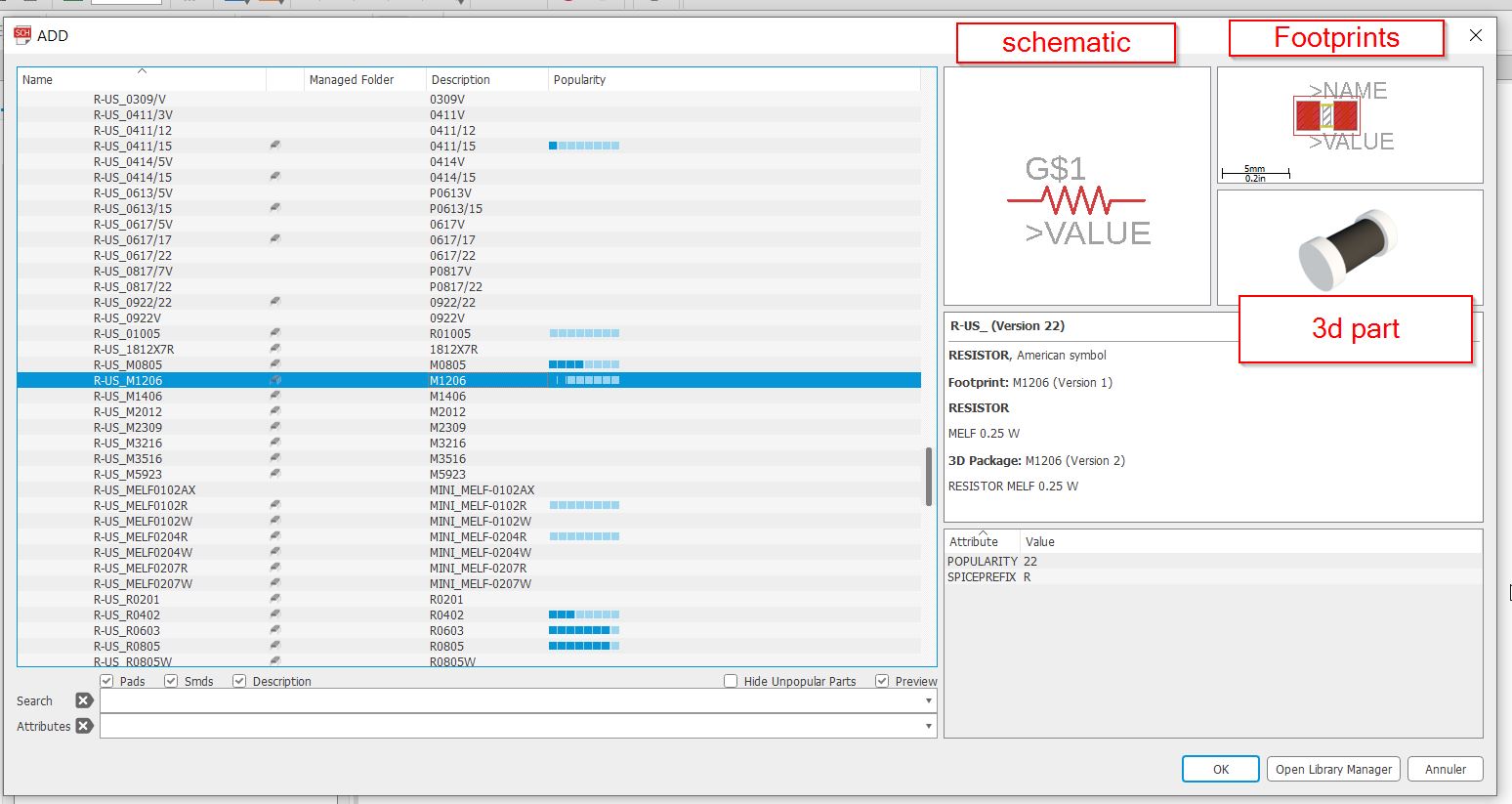
We will add some resistors, go to RCL parts.
There are american and european components.
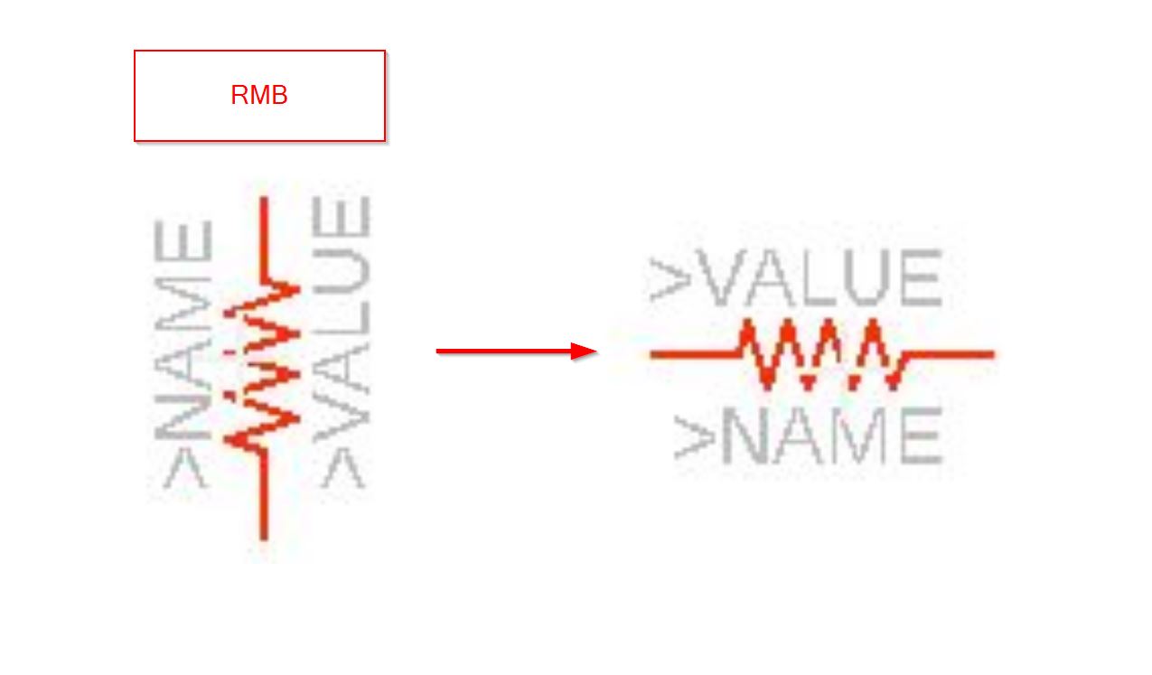
 If you RMB click you will get a90° turn of your component.
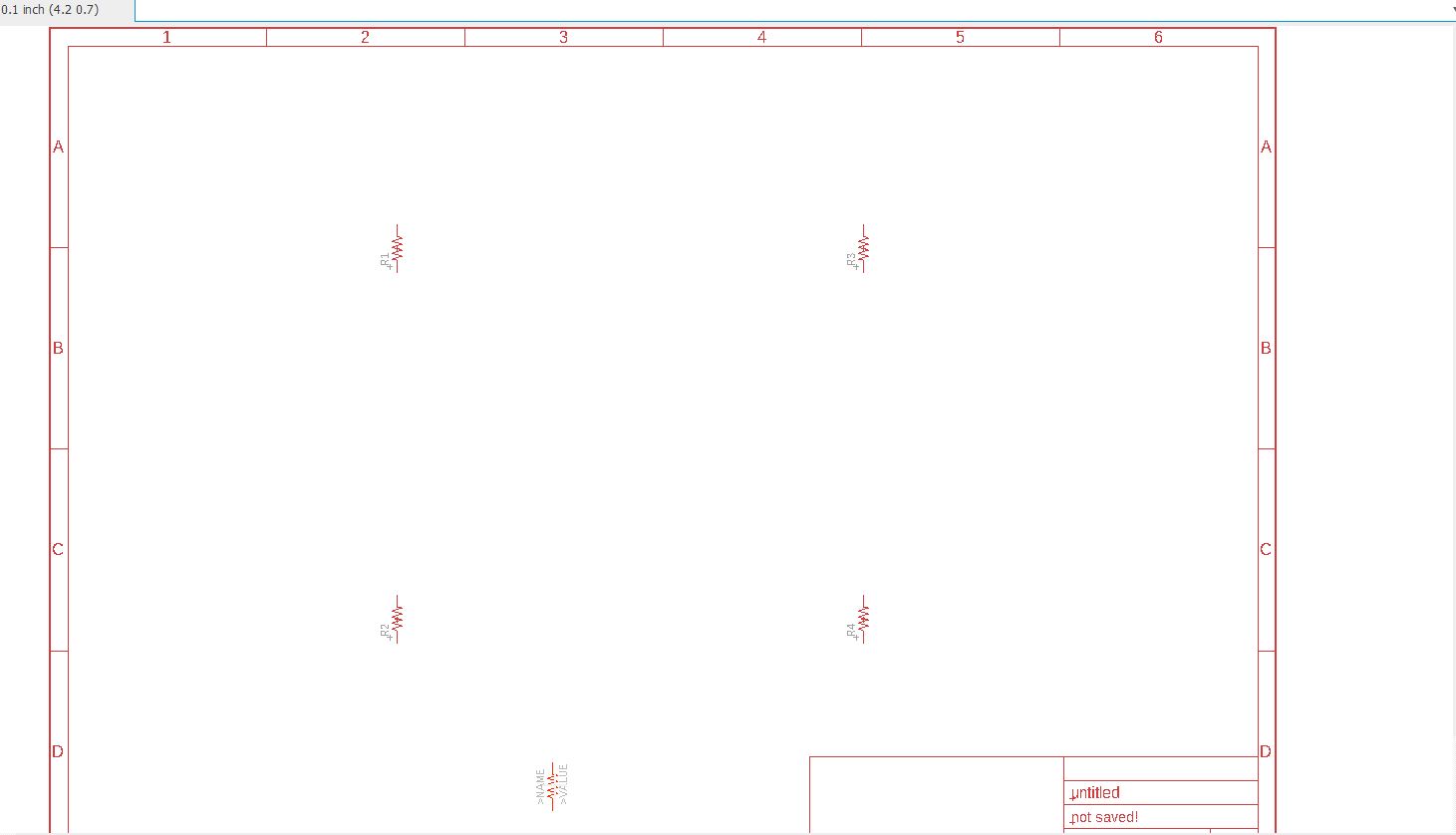
We will get 4 resistors and add timers.
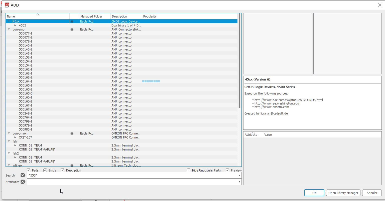
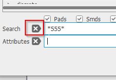
If you look for a part, and you do not have the specific name, just some letters. You have to use the * symbol for your research:
Add the timer.
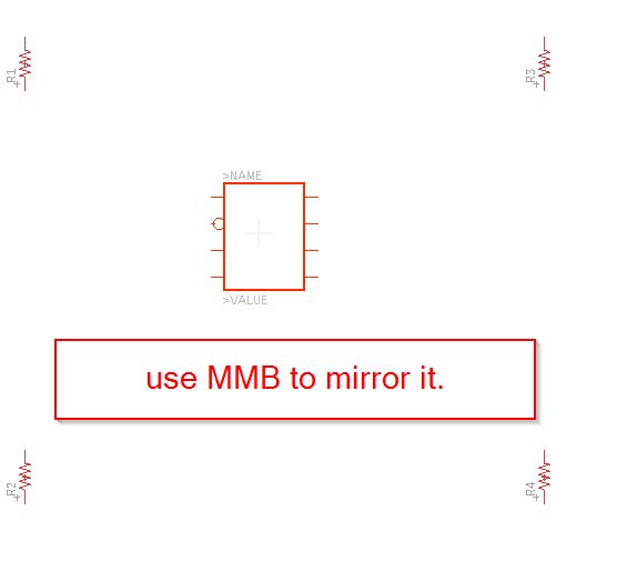
 You can MMB click to mirror the part:
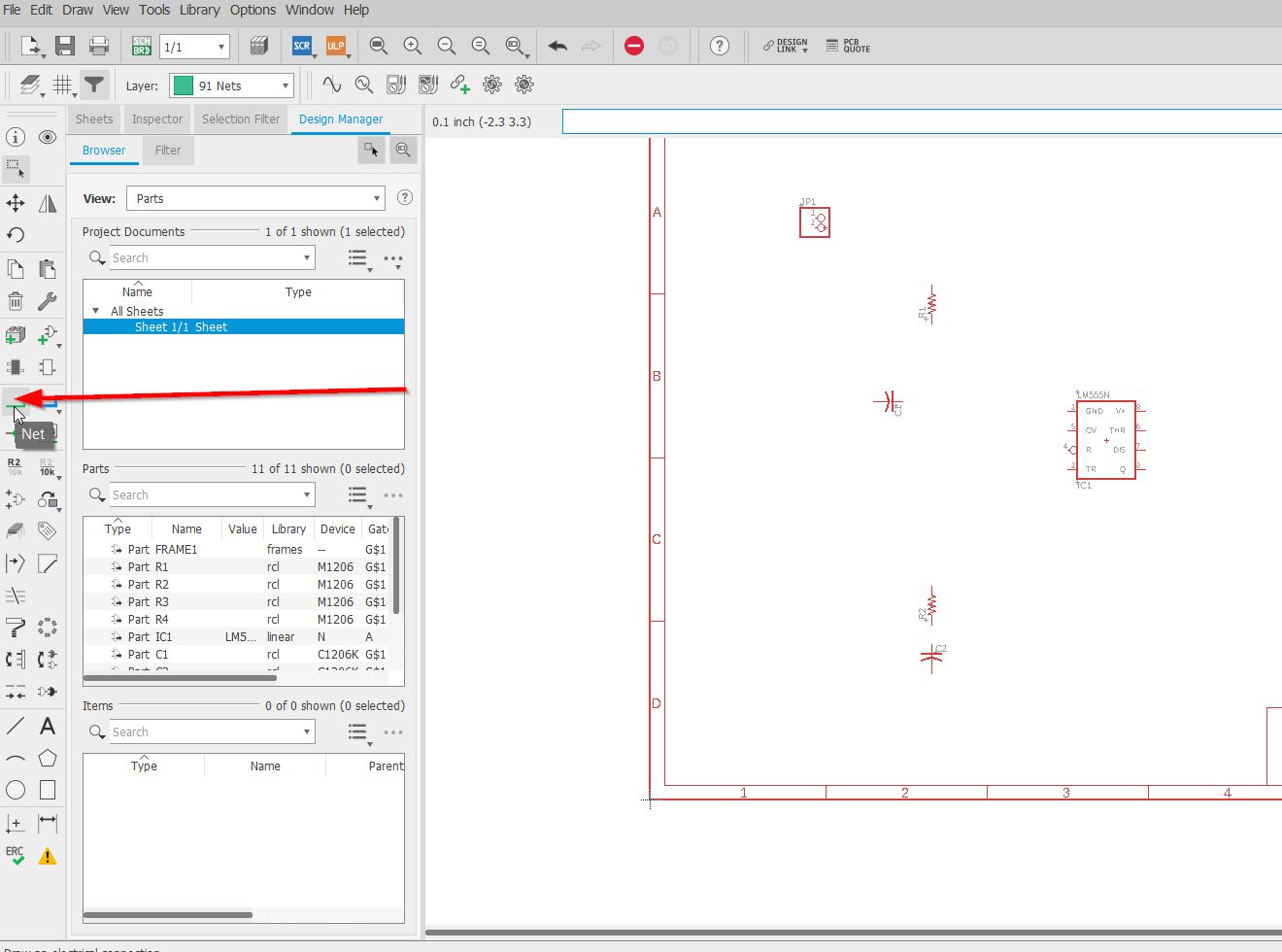
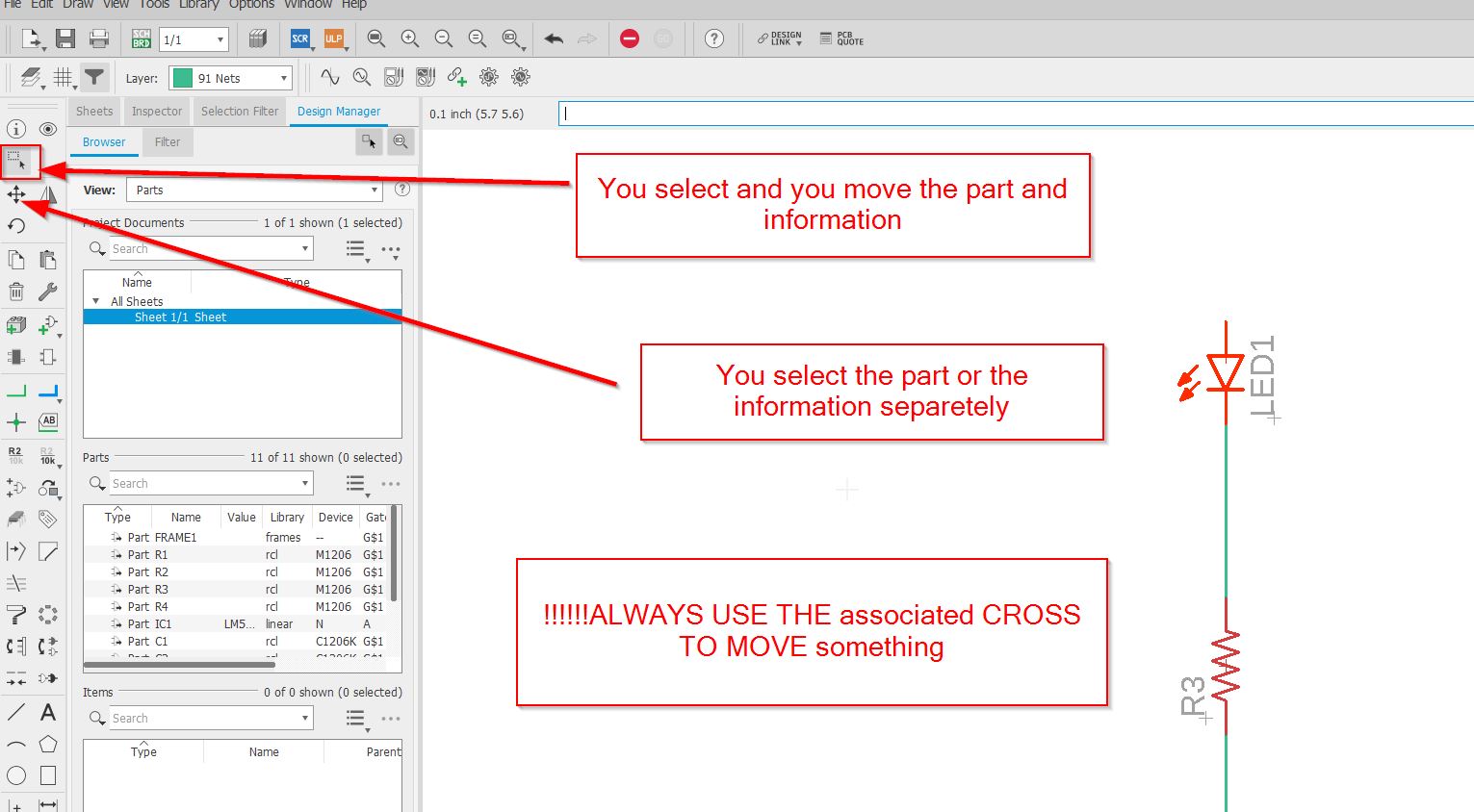
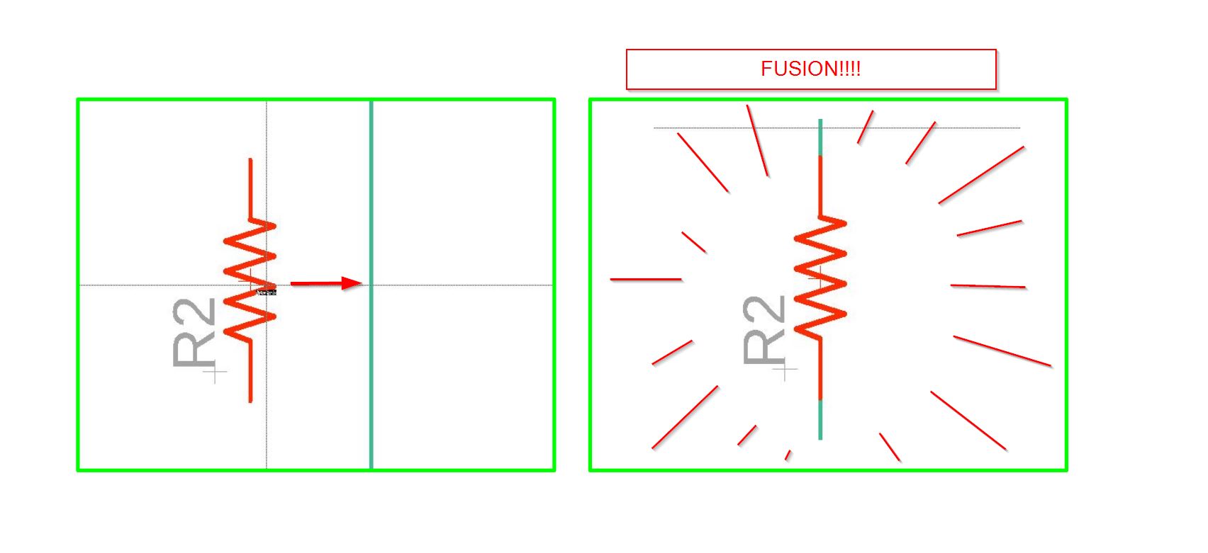
In order to move the whole parts, you select the group tool and click and drag to select all. You will have a small cross. It is important to notice that it is the all thing on this software if you have to move something!!!
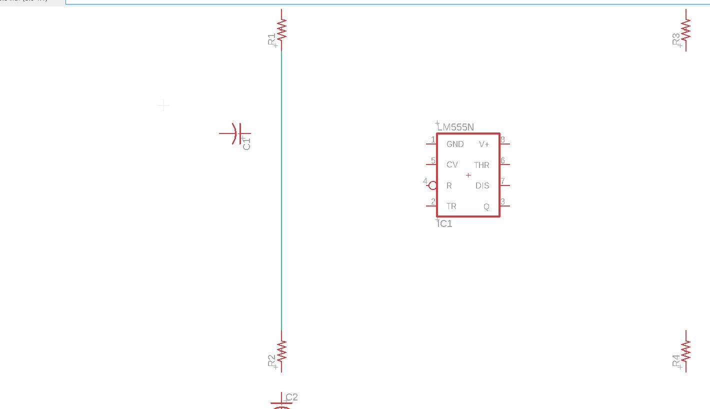
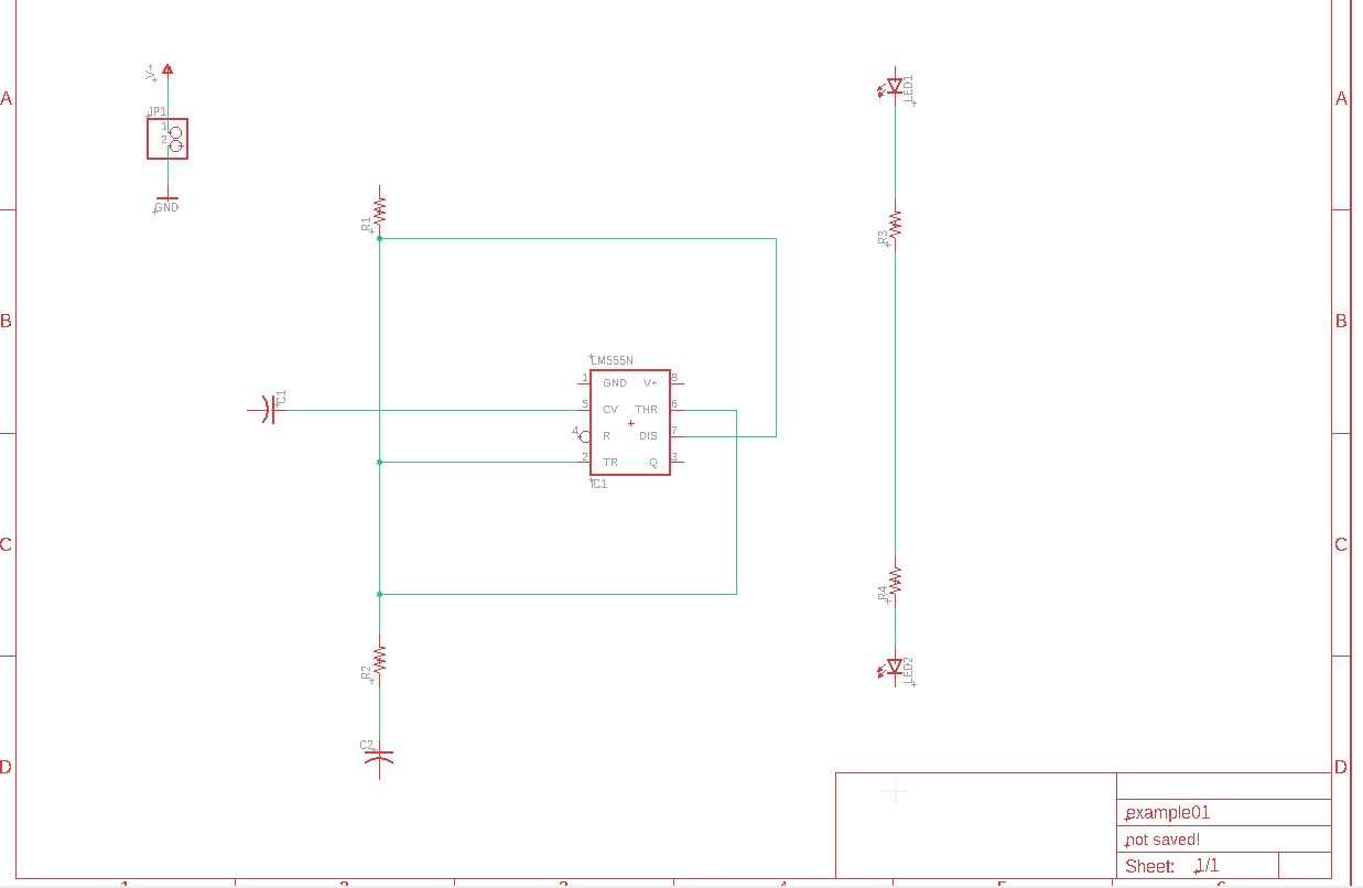
We add capacitors and leds
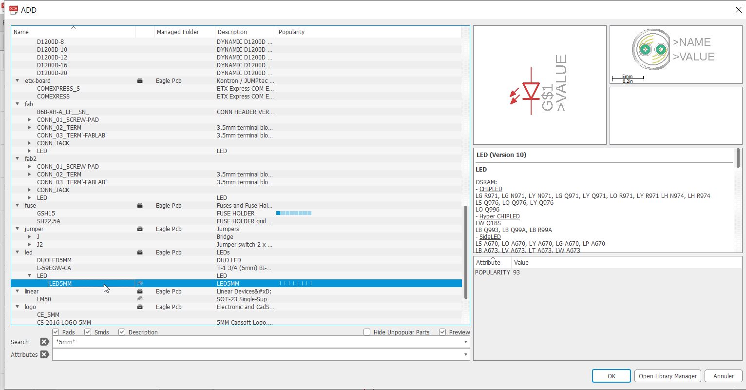
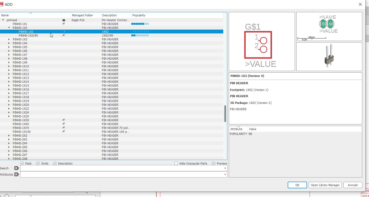
some jumpers. pinhead : PINHD-1x2
Try to get the default grid.
There is a circle around the end of the part, to notice you that you are at the endpoint.
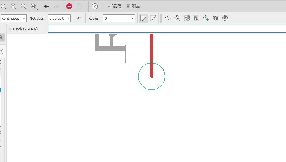
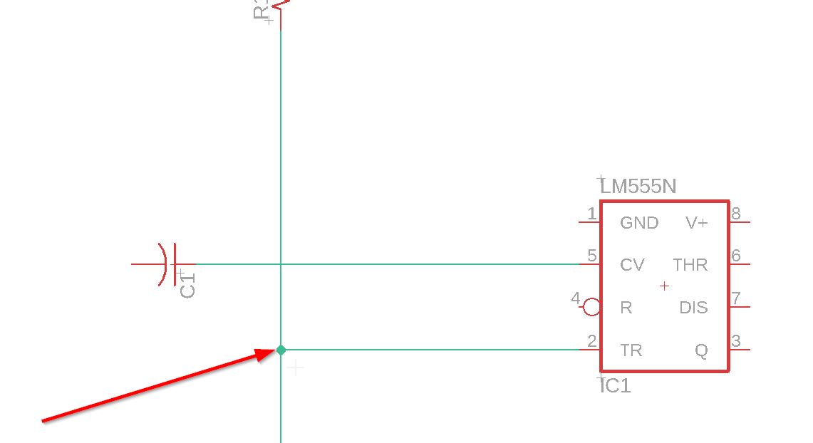
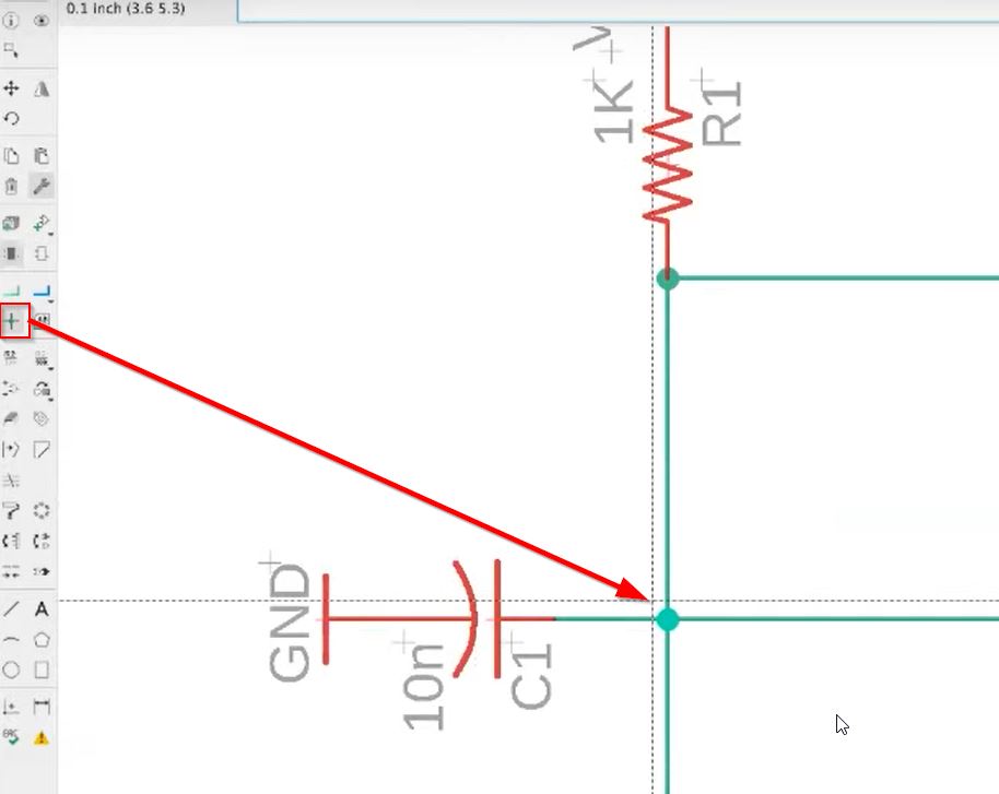
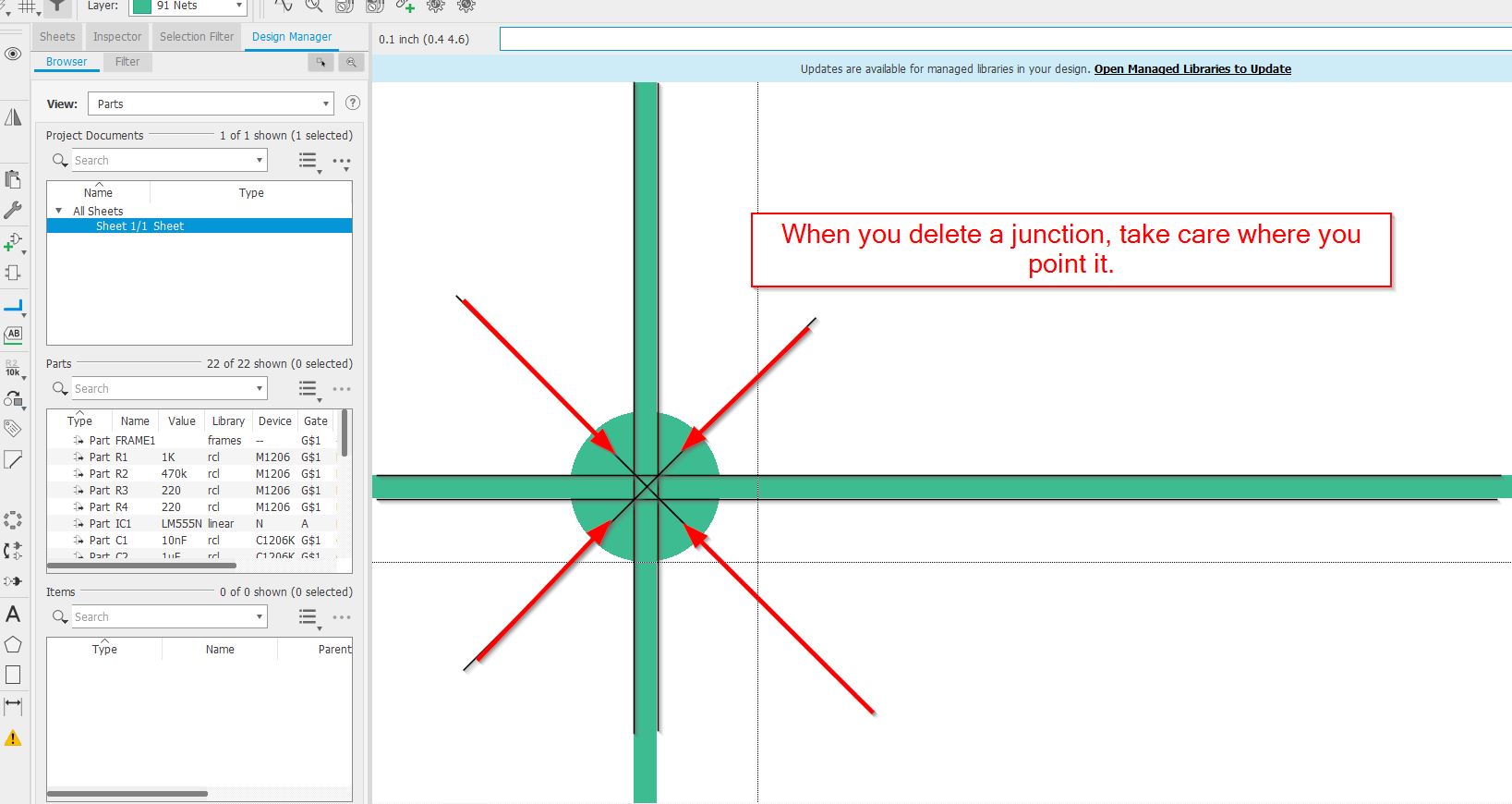
If you connect a net to another net you will see the junction:
C:\github\2023\fabien-jonckheere\docs\images\eagle\junction.jpg
/////Warning, to move separetely items or components, it is important to use precise tools:
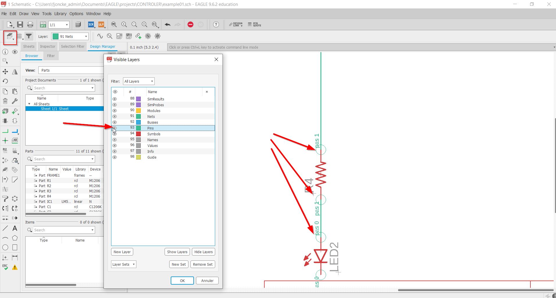
If you have some difficulties to see the endpoints of your components, use the pins layer.
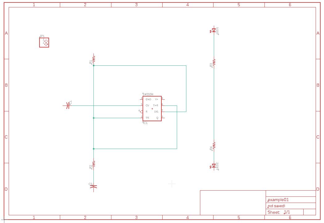
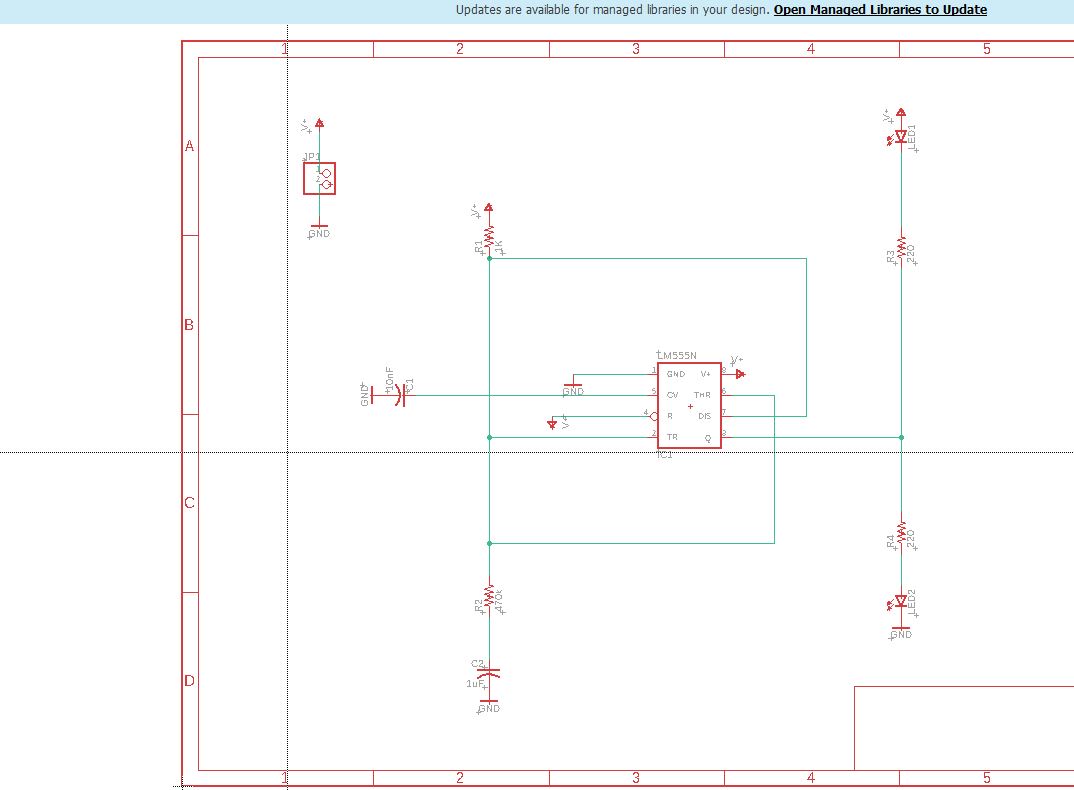
this is an overview of the schematics
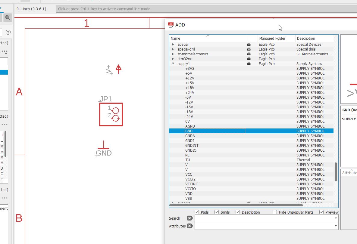
We will add the V+ supply and…
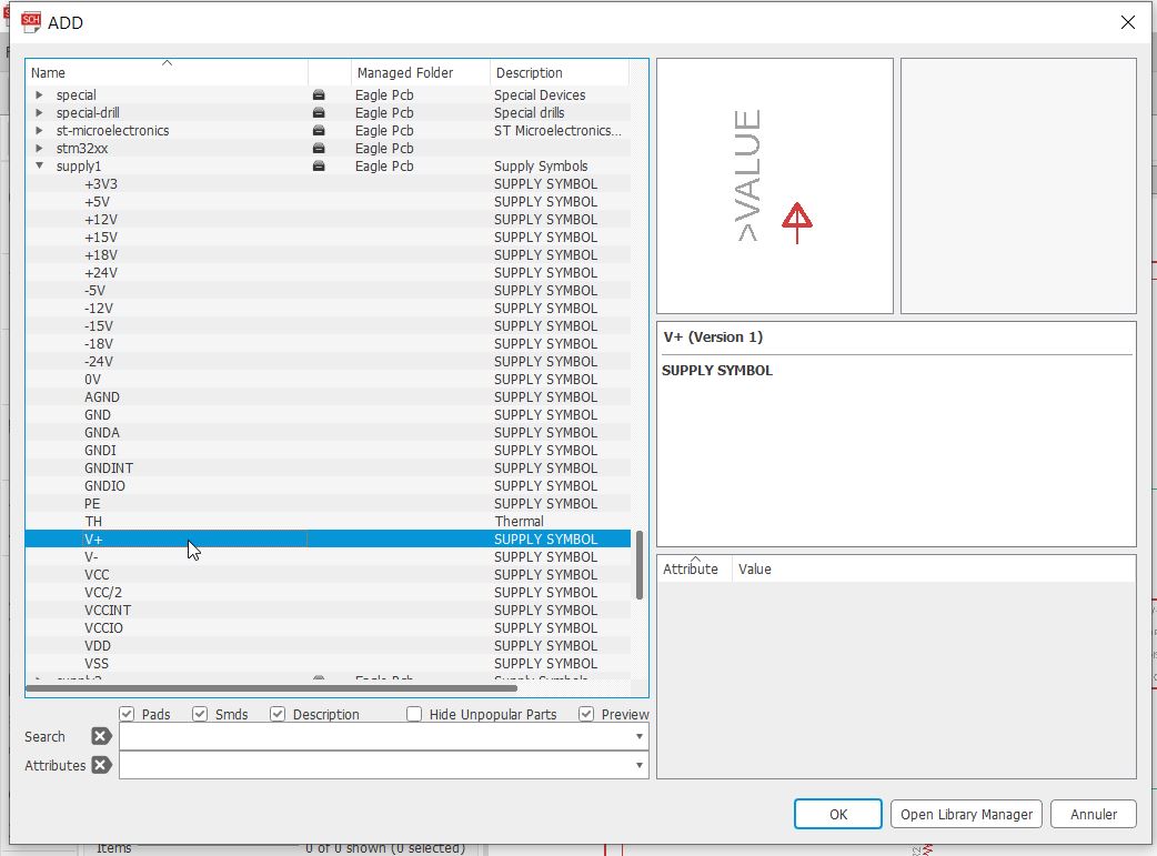
… the ground.
We got that
To copy, you can use the perfect tool.
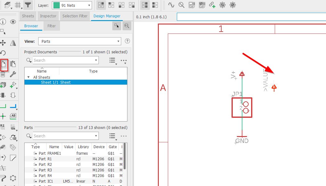
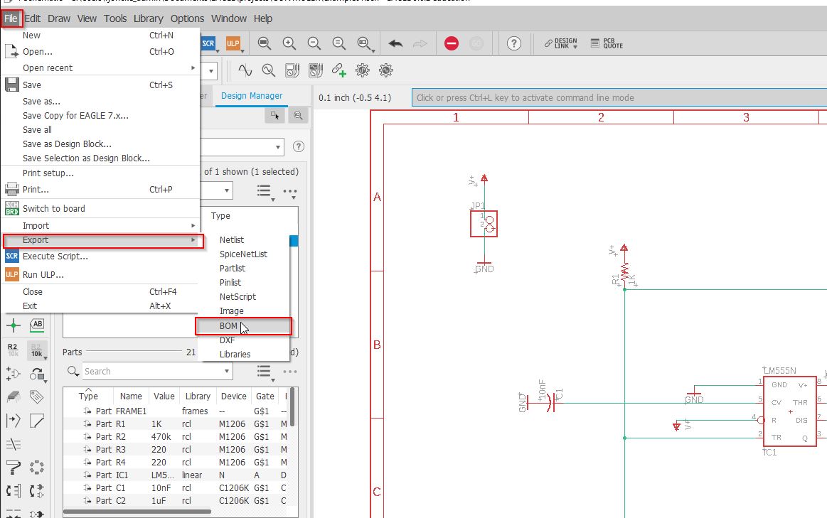
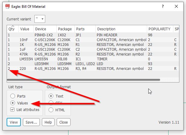
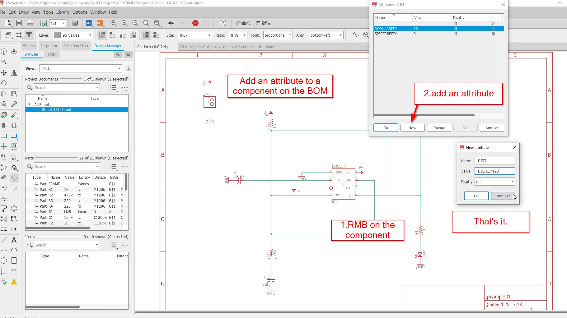
With the BOM option, you can generate a bill of material.
To add specificiations called attribute on the BOM, you right click button on the component, and you will add for example distributor.
Text editor
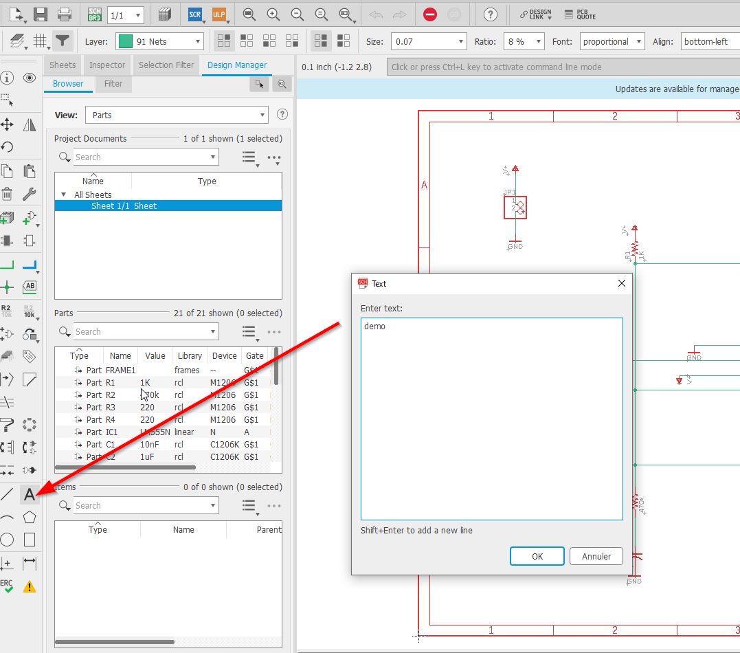
For the text editor, you have to check where you want to have your text out. In my case, I would like get this out of the net layer.
The grid is activated, and the text is moving from 0.1 to 0.1. To avoid that and get a smooth move, press [ALT] key.
If you need to add a junction to cross-over nets, you can use the
Cursor
To get a more precised cursor, you can find a full horizontal and vertical one.
junction selection.
Eagle is sometimes a bit too tricky. To delete a junction, you need to be at the right place. It is sometimes annoying…
Moving parts
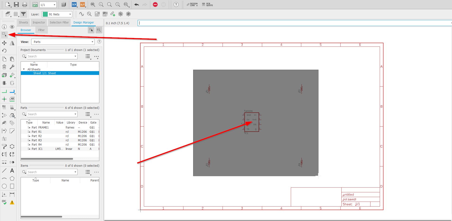
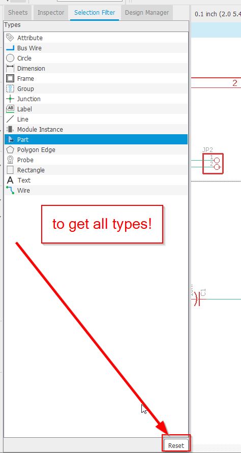
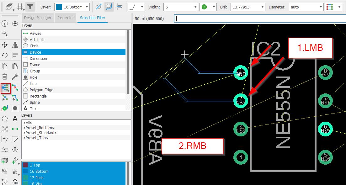
As a beginner, it is important to know that you can filter your selection. There are four tabs: sheets/inspector/selection filter/design manager. Go to selection filter, click on part and select your part
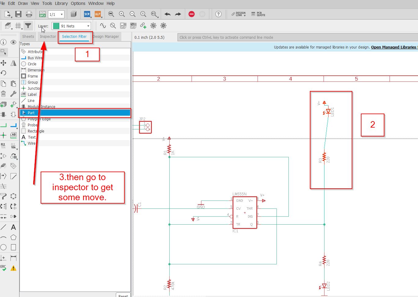
Then you have these options to modify your components.
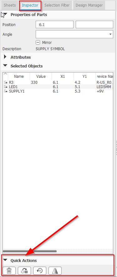
You can delete, rotate, mirror your selection.
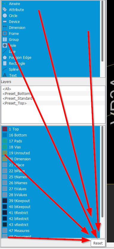
//////// WARNING //////// For any further selection, you have to [RESET] your selection filter:
Adding parts on net:
This is quit easy, just move and drag the component to the net, it will be assimilated to it.
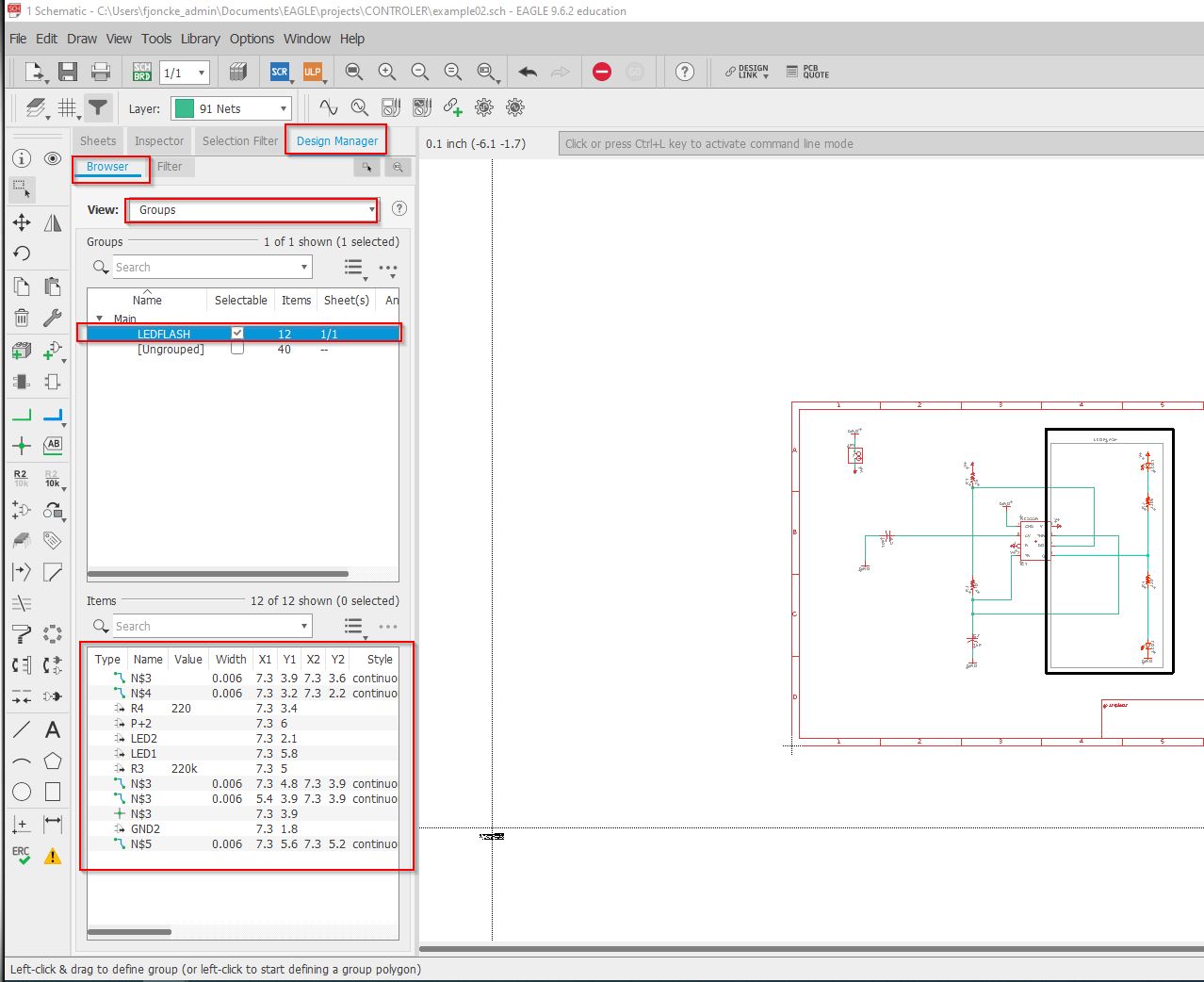
Group
When you have to select or move couple of parts, it is smart to use the group function. You select the components (use the selection filter for that), RMB the selection and choose New group
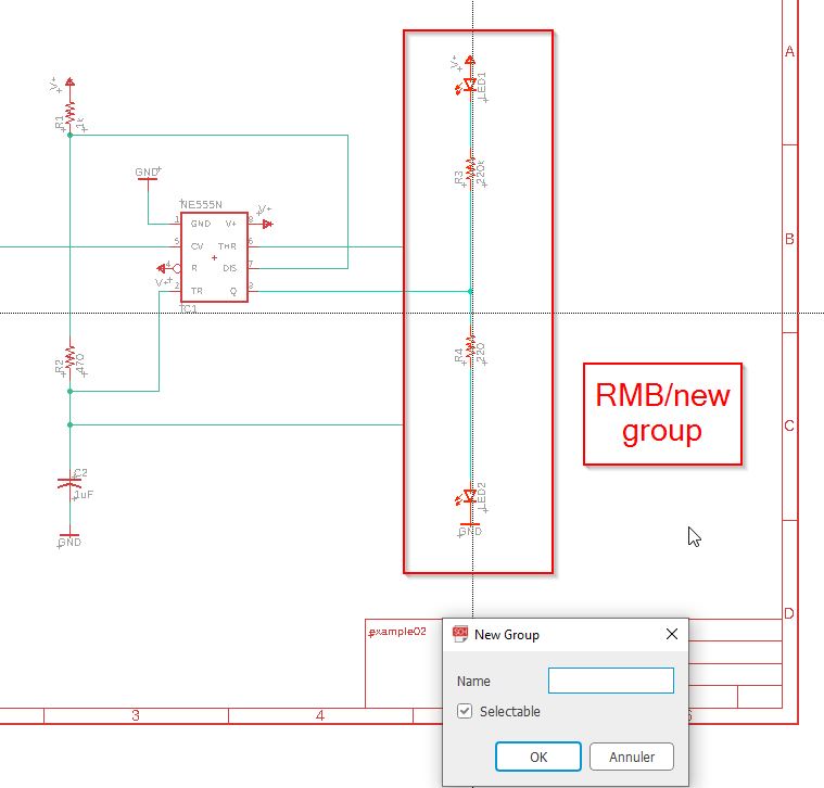
Name your selection. (Here it is LEDFLASH), You will have the full detail by clicking the design manager tab and select the browser. You can select groups n the drop-down menu.
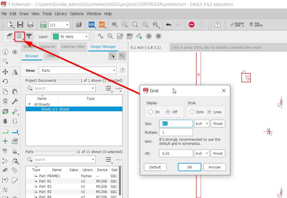
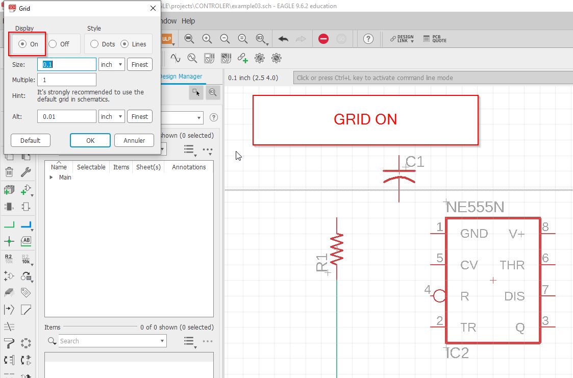
Grid on/off
Sometimes it is convenient to have or to avoid the grid. Go to the main toolbar view. And select grid from the drop-down menu. You can define and visualize it.
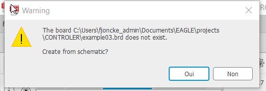
Converting your board into a schematic:
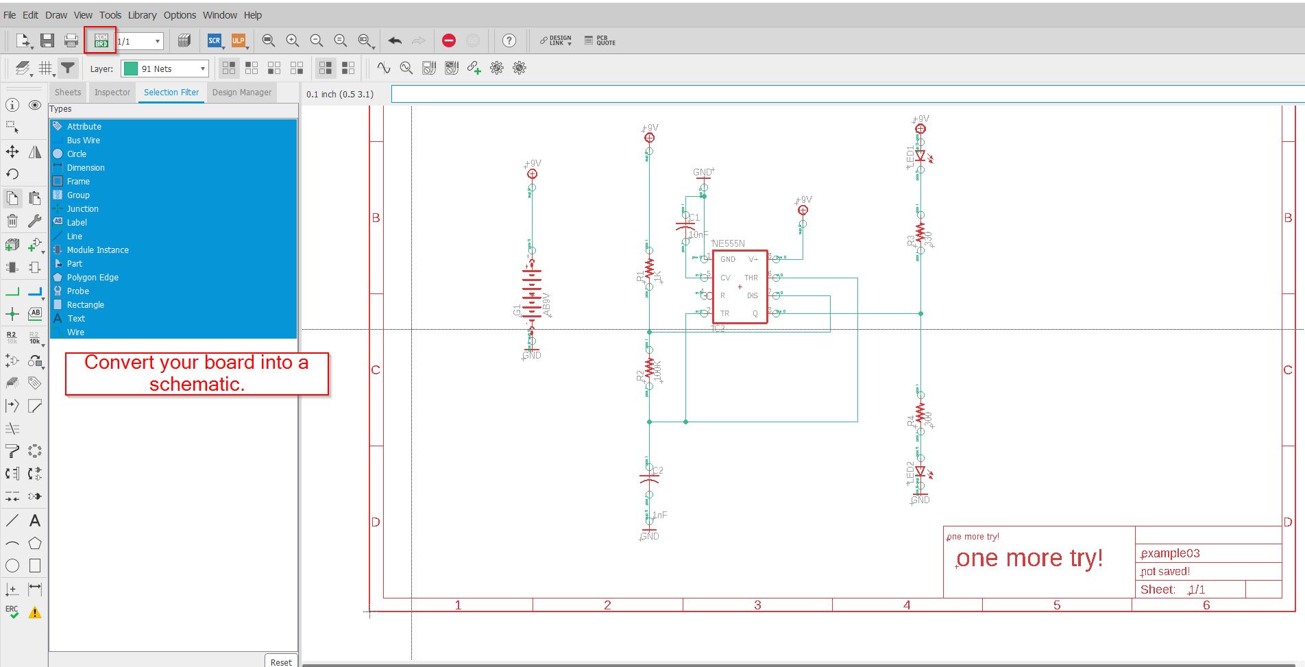
If the board file is not created, it will invite you to generate it:
You will get the components in a black background:
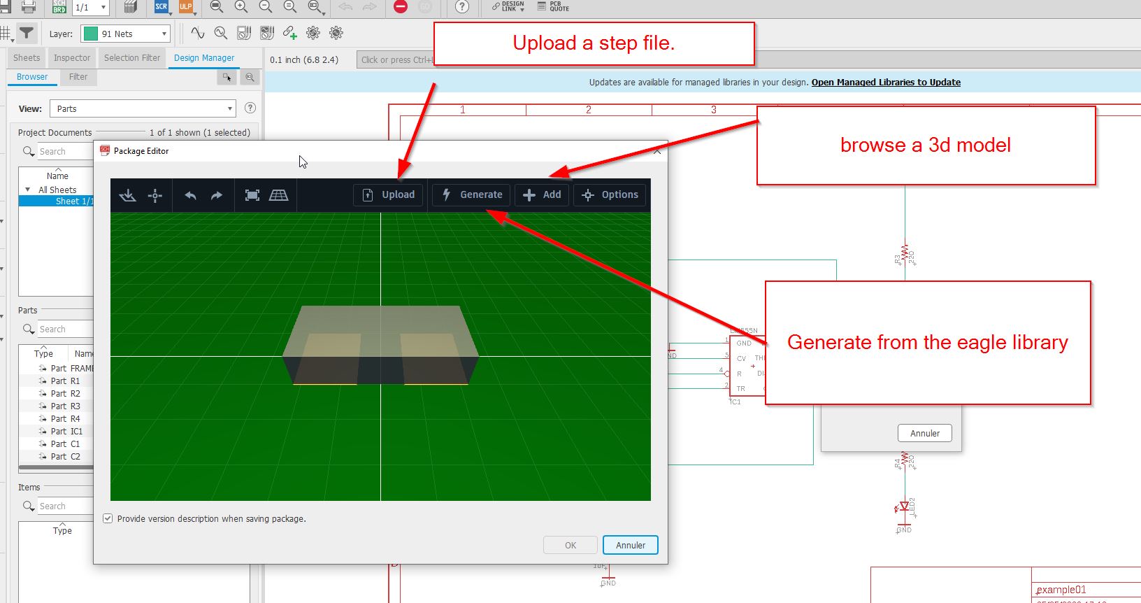
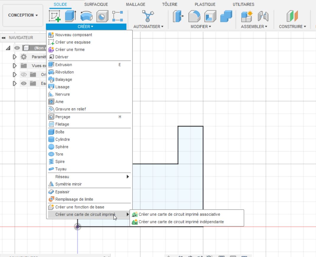
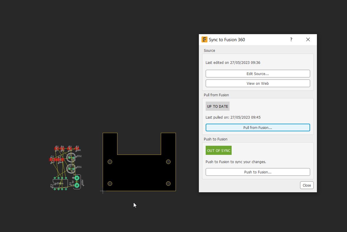
EAGLE TO FUSION 360
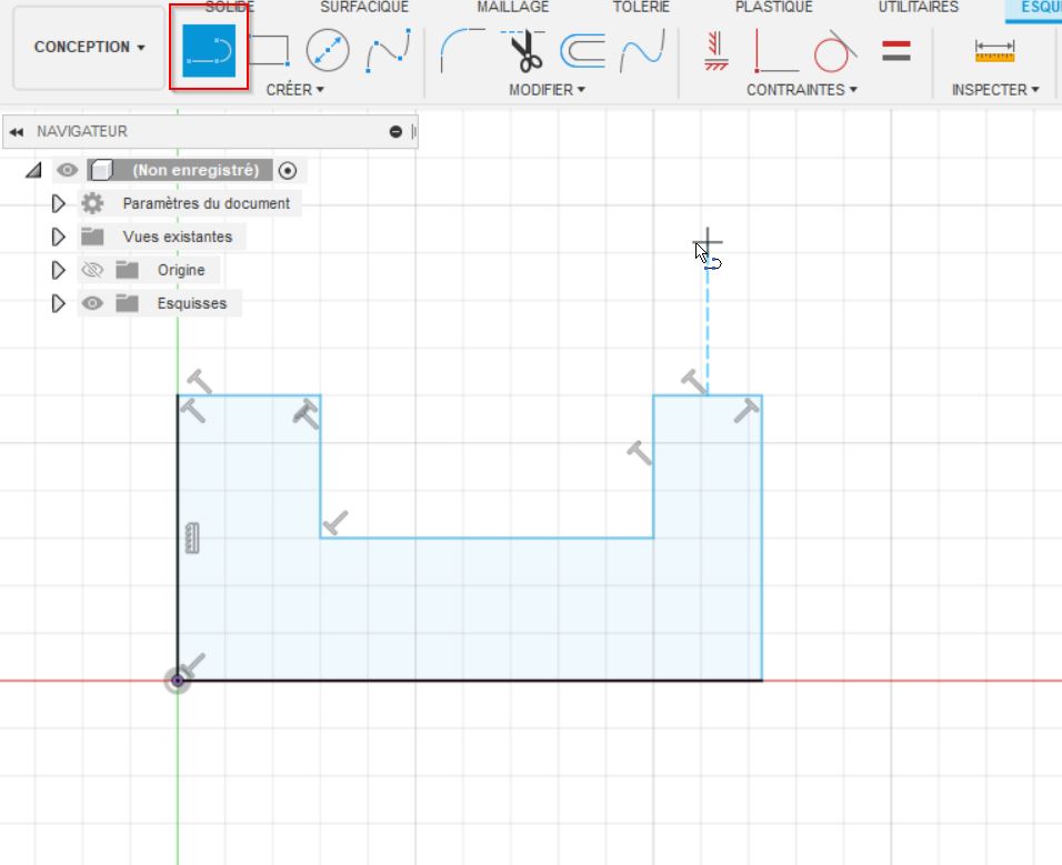
Create a new folder ( Eagle Example) and use the sketch command, select the front view. You can start to make your outer edges of the board.
Use the line tool to create a shape, click on the origin to next point and you come back to the beginning. You will see that the created shape will be highlighted.
To be straight, the constraints command [1] will make equal lines and the [2] tool will get vertical or horizontal ones. For this tool, if you need to have a point at the same level of a line, use the [2] tool by clicking the line and the point.
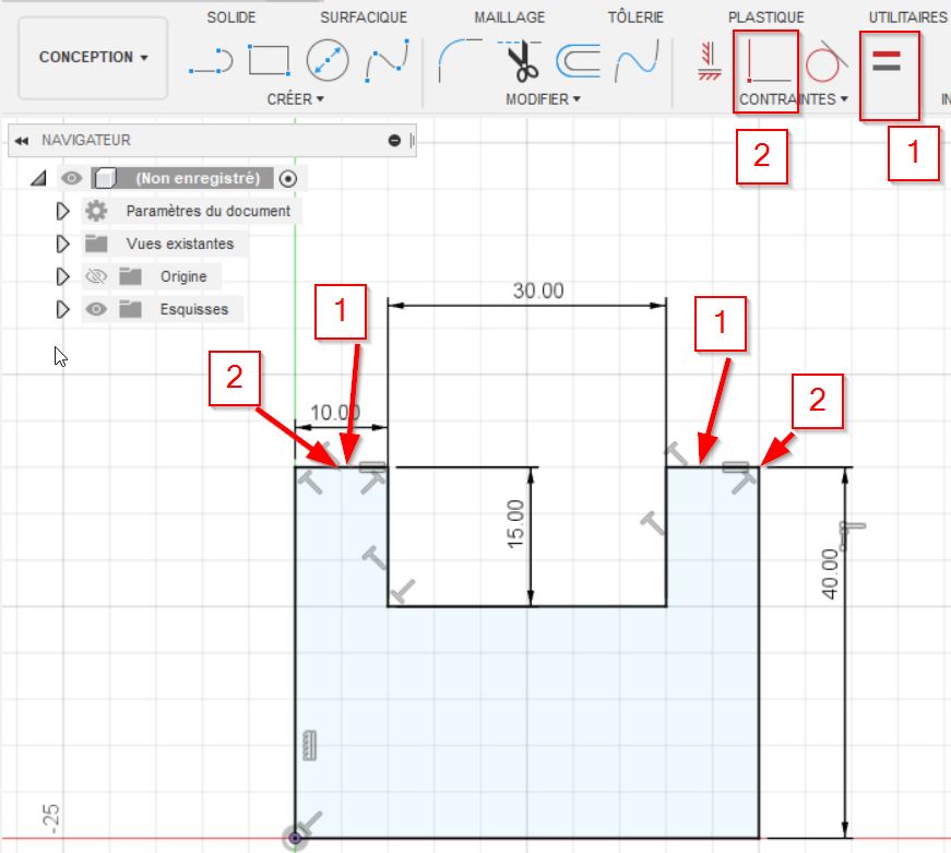
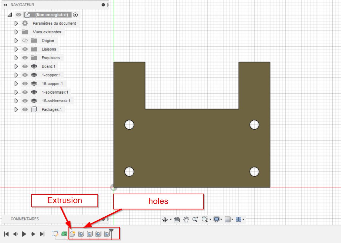
I have added holes to maintain the board.
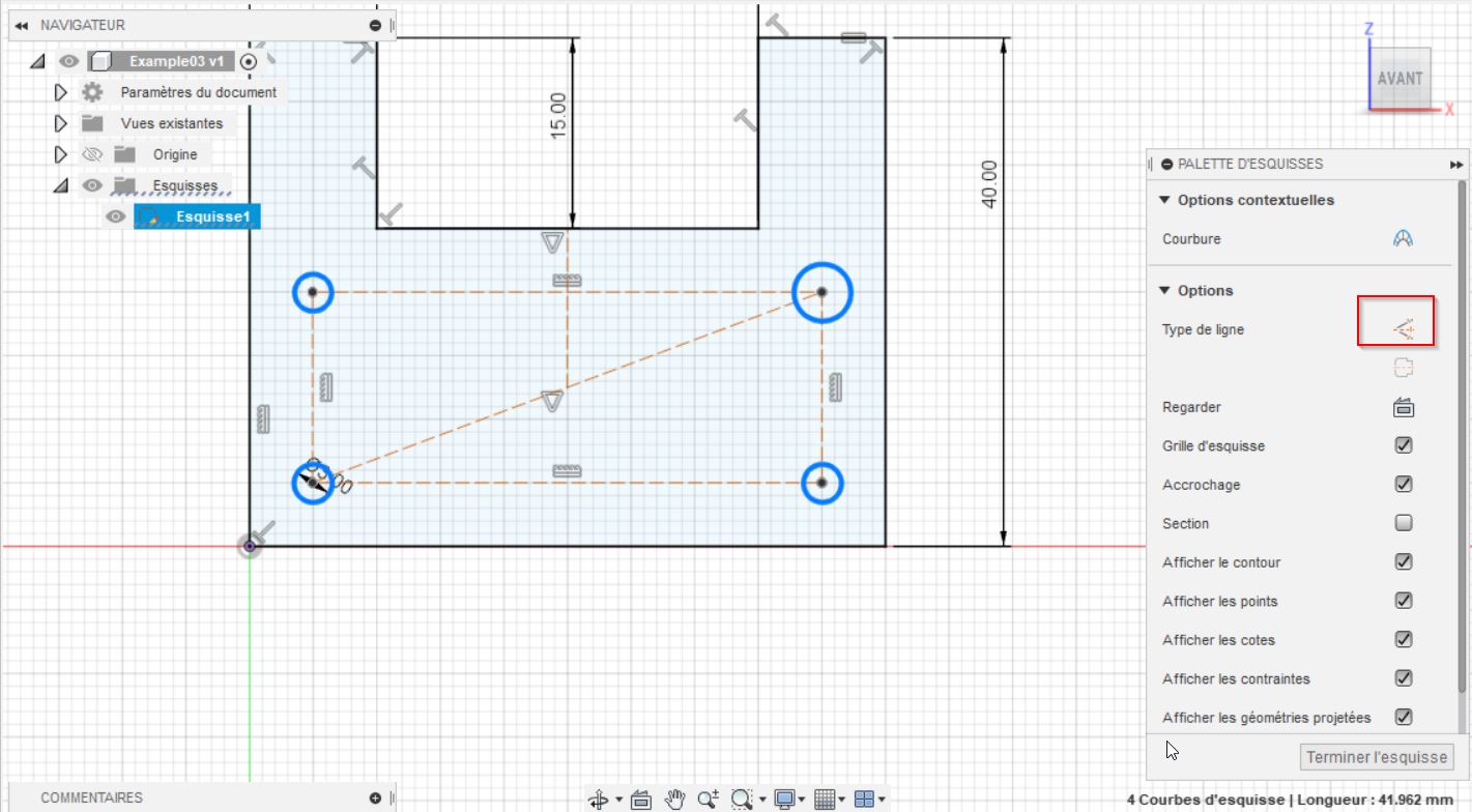
The shortcut [D] provides dimensions, you can find it at the “create folder” When it is dark, the sketch has all required dimensions, you can use the “create PCB” function. Use the independant option.
Select the profil and the origin of your PCB. You can easily change the options: point, directions.
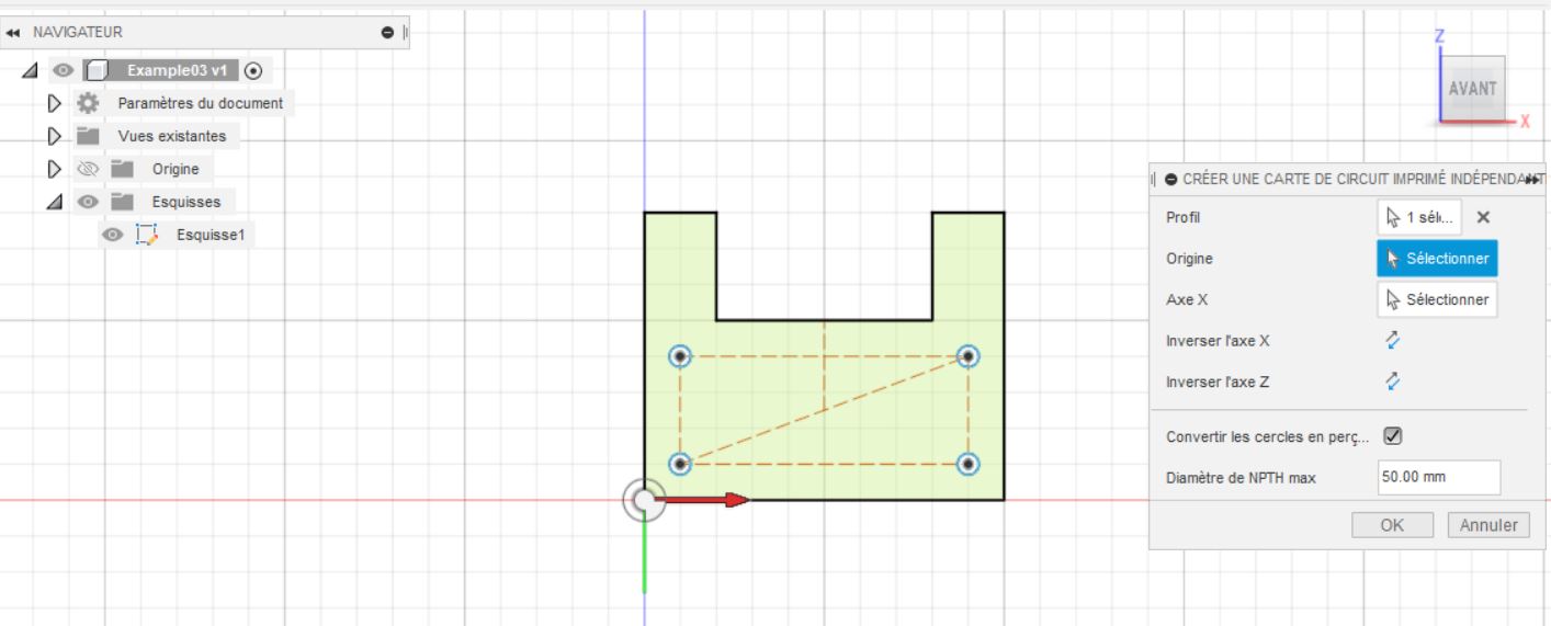
The extrusion and holes are directly converted to PCB functions.
Get back on EAGLE:
Click on the fusion 360 tab, and link to an existing fusion 360 design.
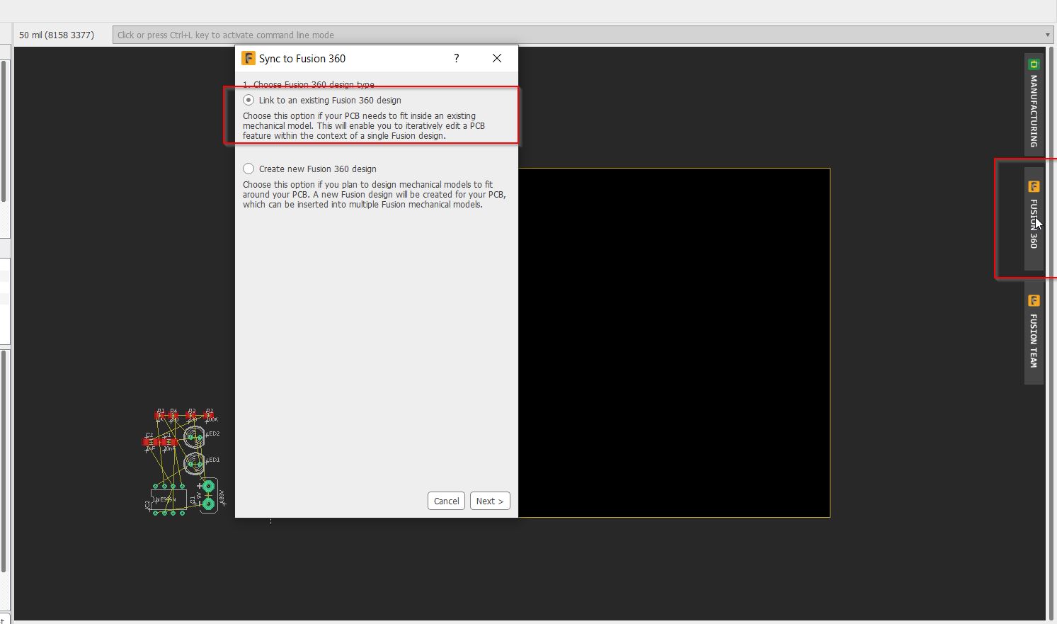
Follow the options:

And finally PULL FROM FUSION:
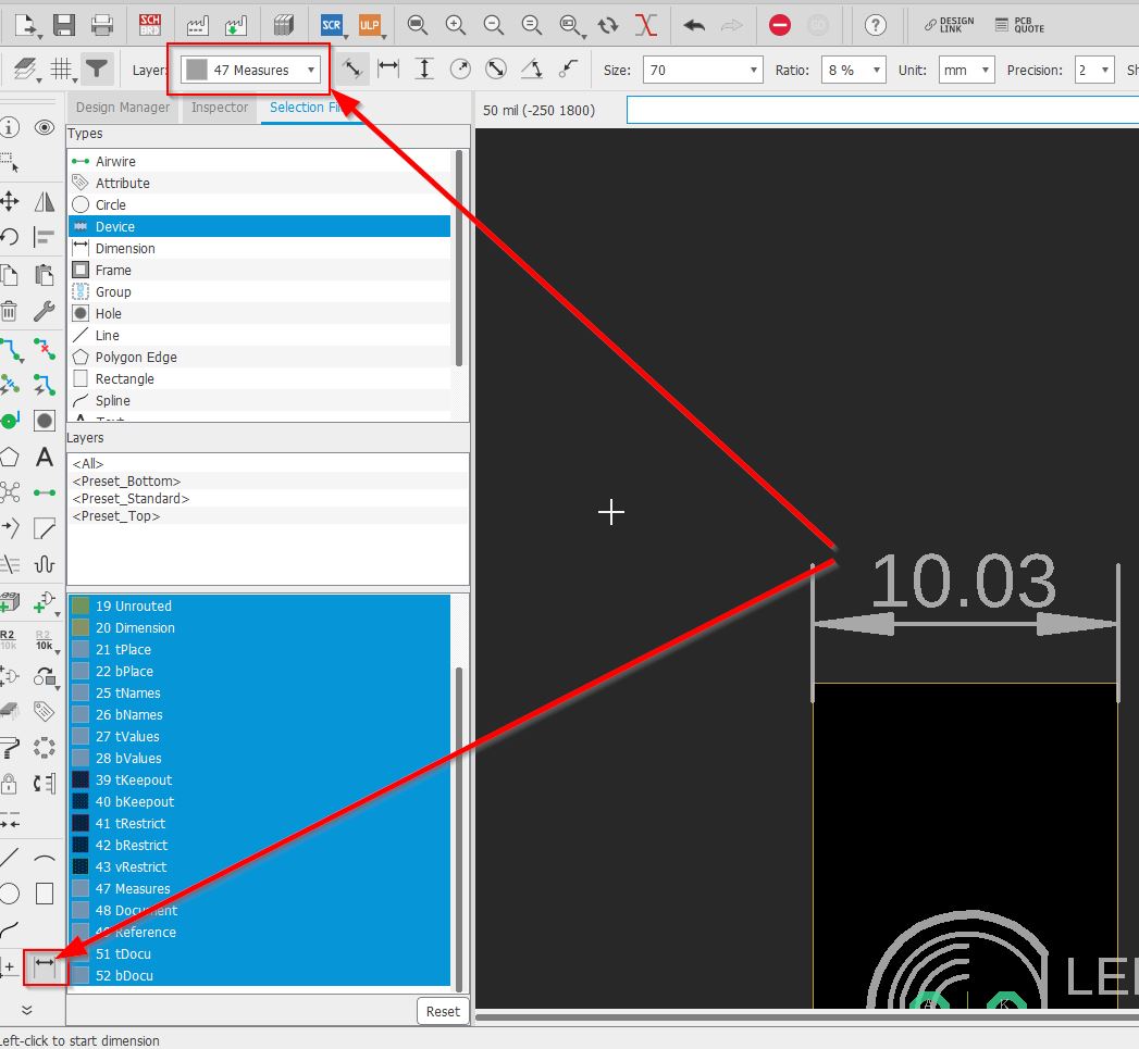
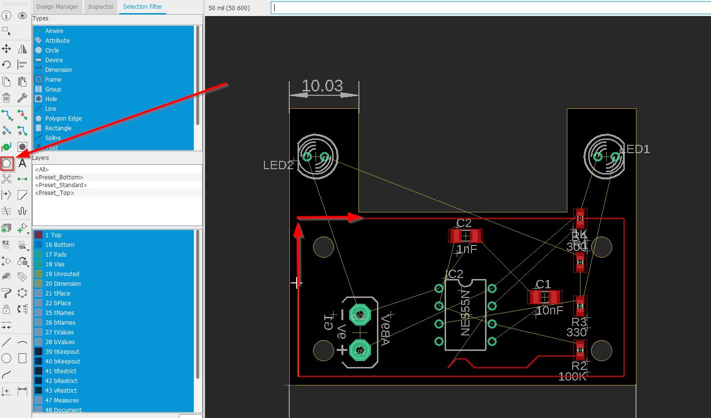
As a beginner, it could be quickly the mess to move items, use the selection filter to get only your devices:
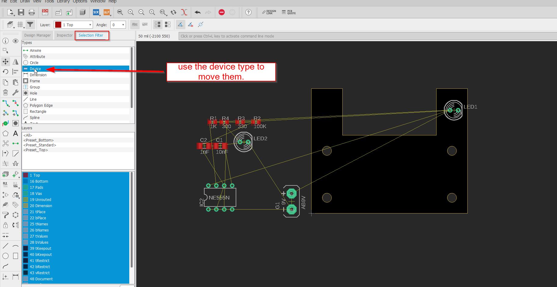
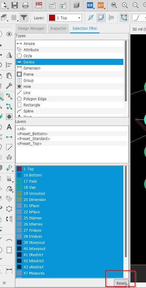
/////// WARNING/////////
It is good to know that if you want to cancel a selection for anything ( components research or this selection filter) you need to click on reset!!!!
Eagle has some tricky operations, and sometimes it makes me crazy. That’s why I write everthing I found down.
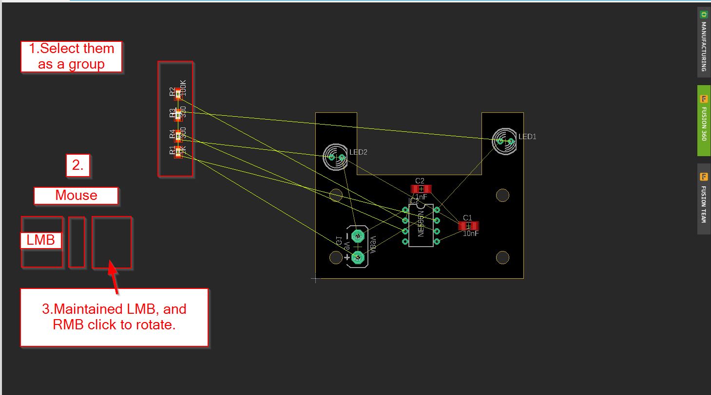
To rotate a group, you do not only select and rotate (which is common on 2D softwares such as inkscape)
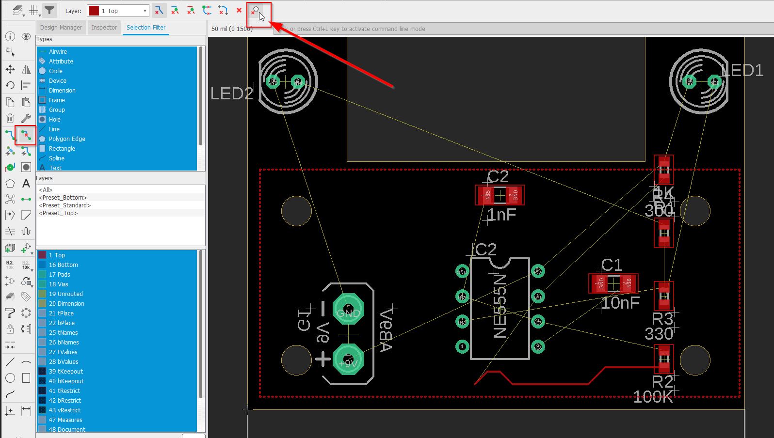
When you are far for the design, use the zoomtofit function.
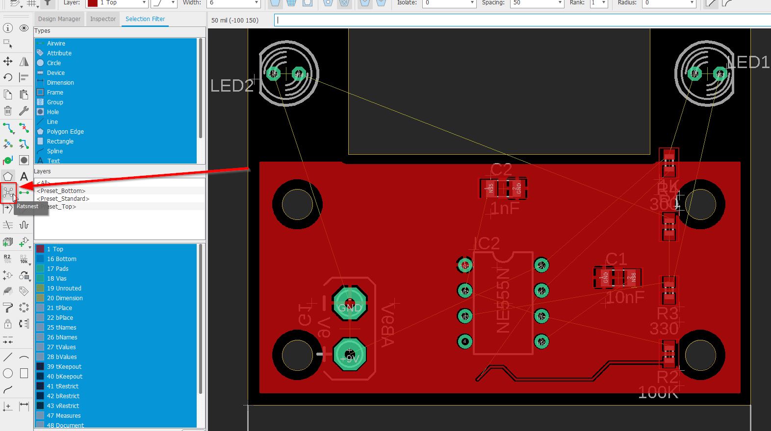
After a while, you have moved components, and the net can be regenerated by using the rastnet process:
When you 2d draw, it is always beautiful to have same spaces between components. You need to know about the alignment functions.
You better get organized for the attributes as well. They are informations related to the components. When you rotate components, they follow the move. So you can reorganize them as well.
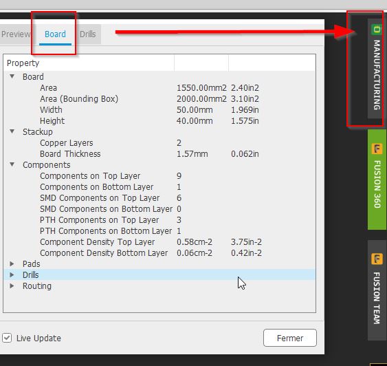
I do not really like the dimensions functions of EAGLE, better to be straight on Fusion and then you get back to Eagle. But It is possible to add measurements.
Dimensions and informations can be found on the manufacturer tab.
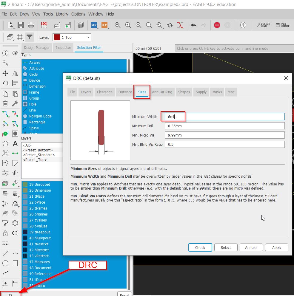
You can start to wire your board circuit, but first look at the thickness of your presets. Here I will change 6 to 12mil. You have to check the design rules check function. You define all your presets for your drawing here.
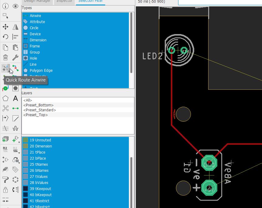
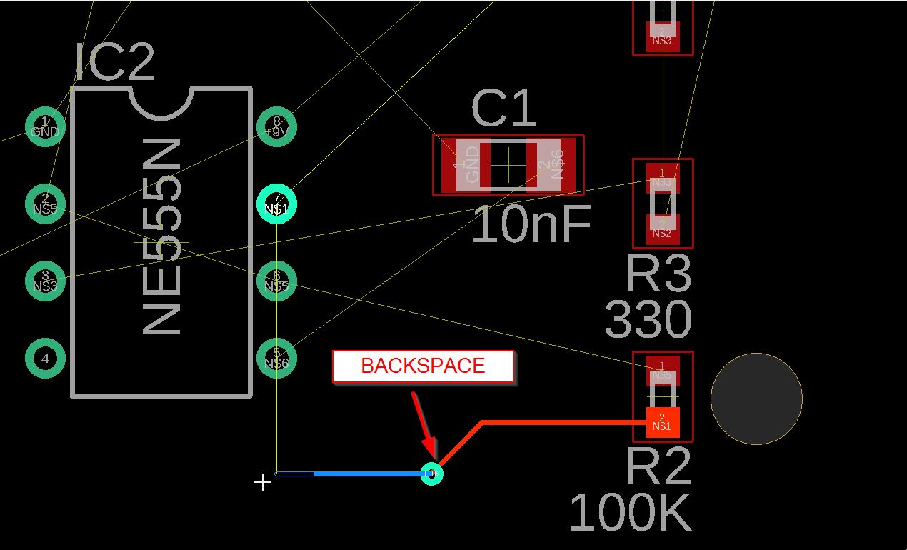
When you have simple paths to make, you can use the quick route airwire tool. Here I have clicked on the LED and the - of 9V. The path comes instantanetely.
/////////// SHORTCUTS:
[backspace] to cancel a route and get back to the previous route. [SPACE BAR] to add a VIA to the end of your route.
When you use this option, the via will guide you from the top layer to the bottom one. The wire will be blue.
It is possible to have a route multiple airwire. You LMB on the pins you want and then RMB and start your route.
You have different options, you can easily get them by writing “assign” in the command line editor: minspacing - Alt+D incspacing - Alt+S decspacing - ALT+A
(see the informations at the bottom part)
rip up function
This function has several options. The default one remove segment.
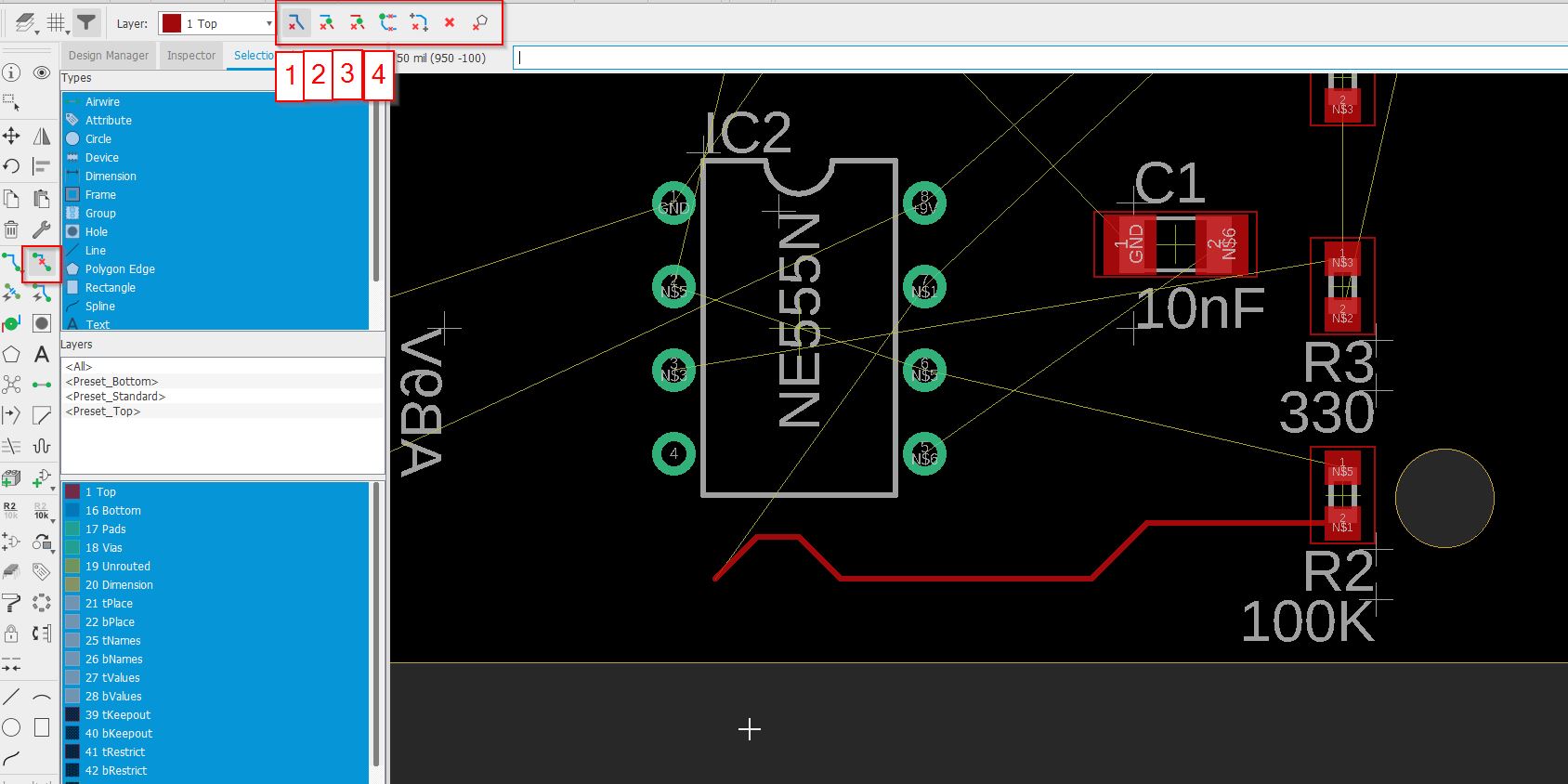
1 just a segment 2 connected copper - delete till the component - top or bottom layer, everything is gone 3 connected copper on same layer 4 signal (not try)
The 5th( which is not marked) is convenient because it rip the wire between two components up. The 6th will remove all wires!! Be carefull!!
/// I was a bit frustrated because the command was not working!! But It rings a bell and thought: you forgot something. I went deeply to what it is annoying on EAGLE. And I remenber… THE SELECTION FILTER!!! I use the reset function to get all default selection.
Create a polygon:
You can easily create different shapes by using the polygon tool.
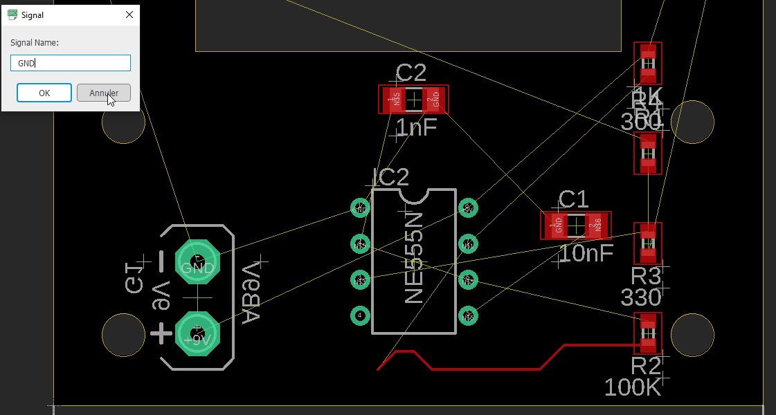 You assign GND to this.
Rastnest will fill the entire shape in. It will create the shape for holes and pins.
How to remove the polygon?
87-ripuppolygon
If you need to remove it, use the ripup command and select the right option.
my board will be a polygon!
It is easy to get the board as a polygon. You RMB an edge of the board, and convert to a polygon by copy the shape.
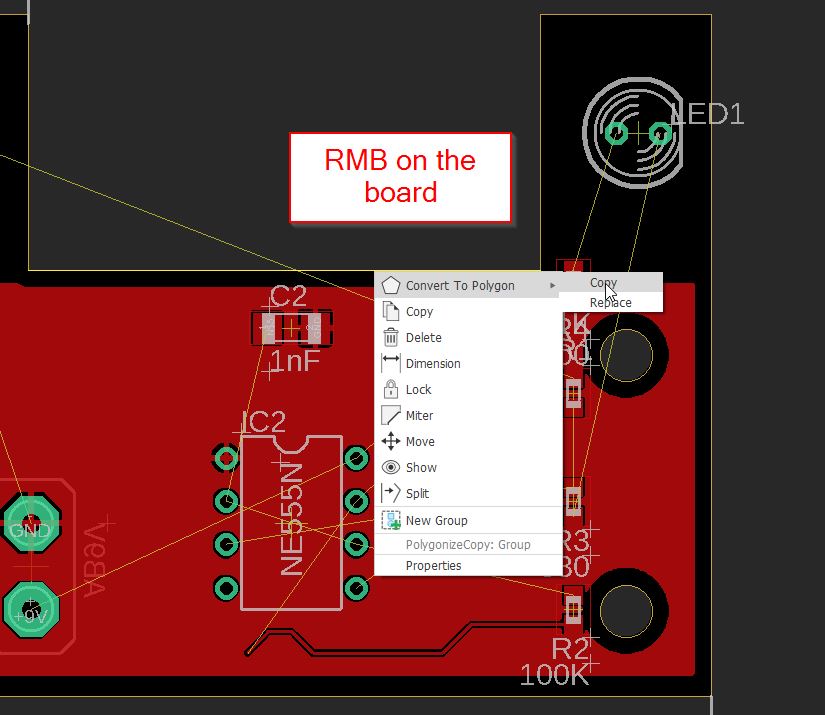
IT will ask you where to copy it, you select the bottom layer. Then you can rastnest, and find the perfect polygon
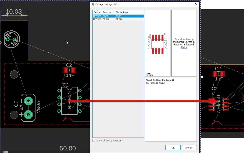
How to change a component?
By using the selection filter, you get the device, RMB the component, choose “package” , not replace.
////////////// WARNING
I have made this change, and I had some problems when I restart my project. “Schematic and board are not consistent”
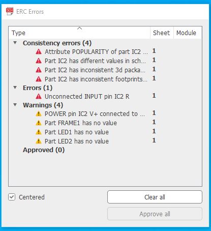
Apparently there was something wrong with the IC2 which is the timer. I came back on the schematic and used the “package” function from RMB. Everything should be clear.
Fan out
I have to go deeply in this field, it seems that
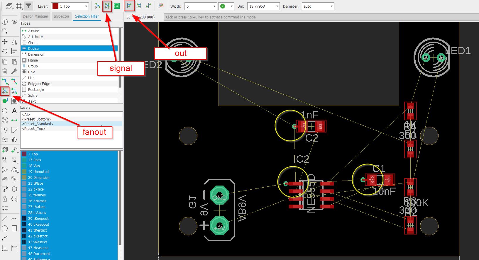
Where GND is somewhere, there will have a VIA.
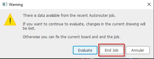
autorouting.
Autorouting is simply a function to route;
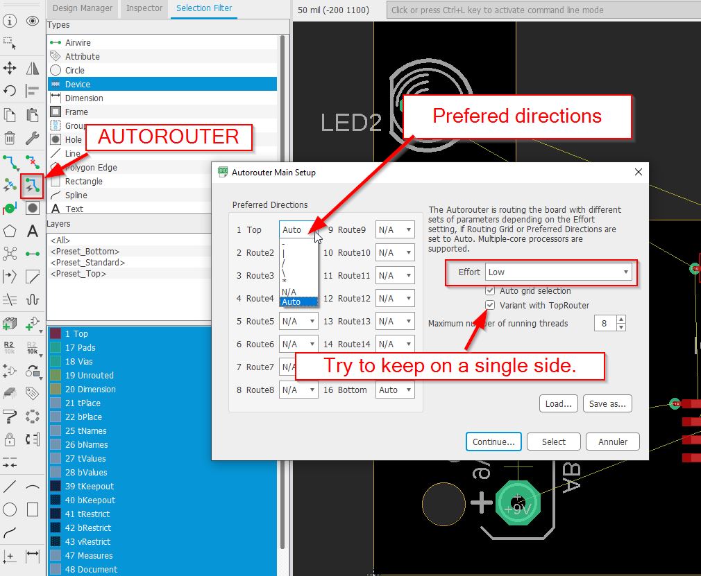
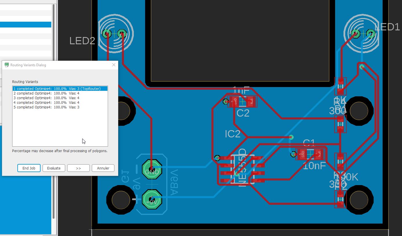
You have different routing variants, select the one you want, (avoid via as much as possible) Click “evaluation” to get an real overview.
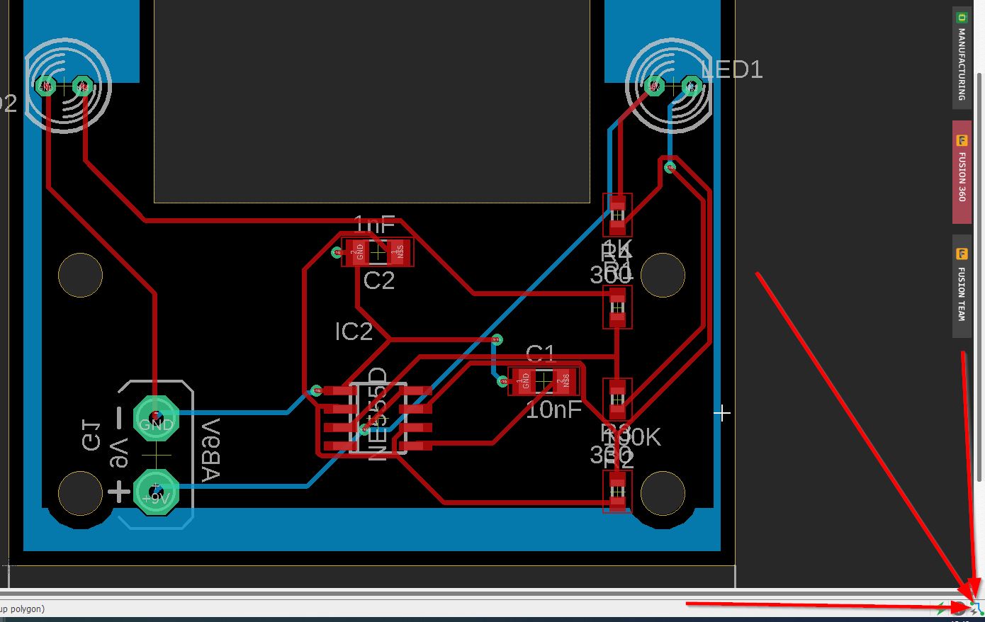
If you are done, click on “end job”.
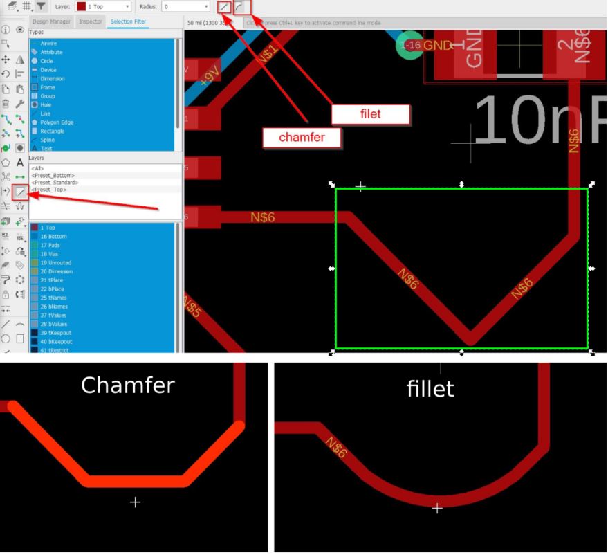
Getting smooth signals.
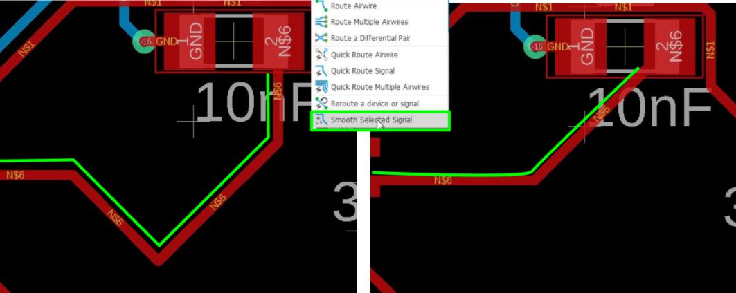
How to miter? (chamfer or fillet)
Design Rules
from MIT
Design Rules define all the parameters that the board layout has to follow. (thickness of routing path, etc…)
The Design Rule Check checks the board against these rules and reports any violations.
The Design Rules of a board can be modified through the Design Rules dialog, which appears if the DRC command is selected without a terminating ‘;’.
Newly created boards take their design rules from the file ‘default.dru’, which is searched for in the first directory listed in the “Options/Directories/Design rules” path. If no such file is present, the program’s builtin default values apply.
Note regarding the values for Clearance and Distance: since the internal resolution of the coordinates is 1/10000mm, the DRC can only reliably report errors that are larger than 1/10000mm.
File
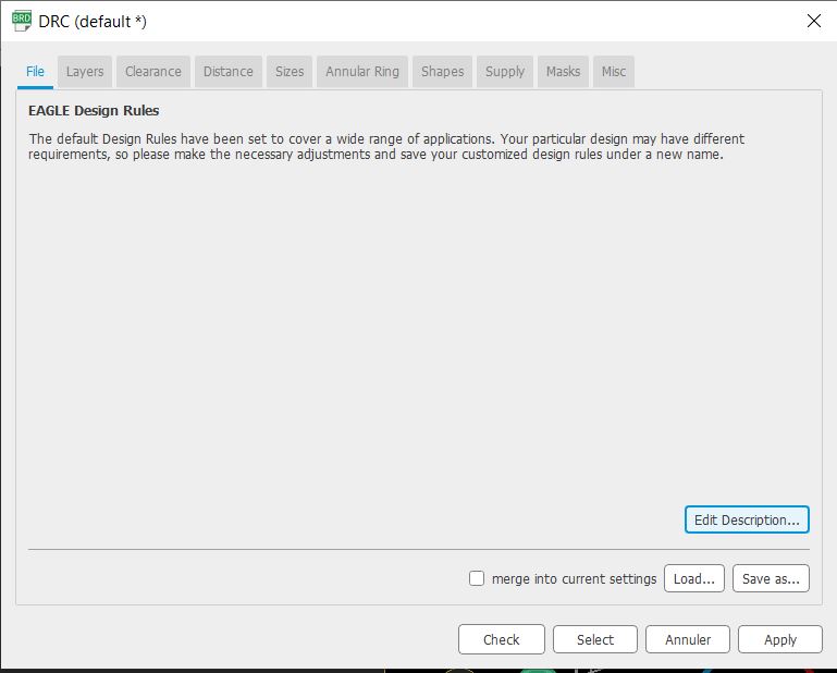
The File tab shows a description of the current set of Design Rules and allows you to change that description (this is strongly recommended if you define your own Design Rules). There are also buttons to load a different set of Design Rules from a disk file and to save the current Design Rules to disk. Note that the Design Rules are stored within the board file, so they will be in effect if the board file is sent to a board house for production. The “Load…” and “Save as…” buttons are merely for copying a board’s Design Rules to and from disk.
Layers
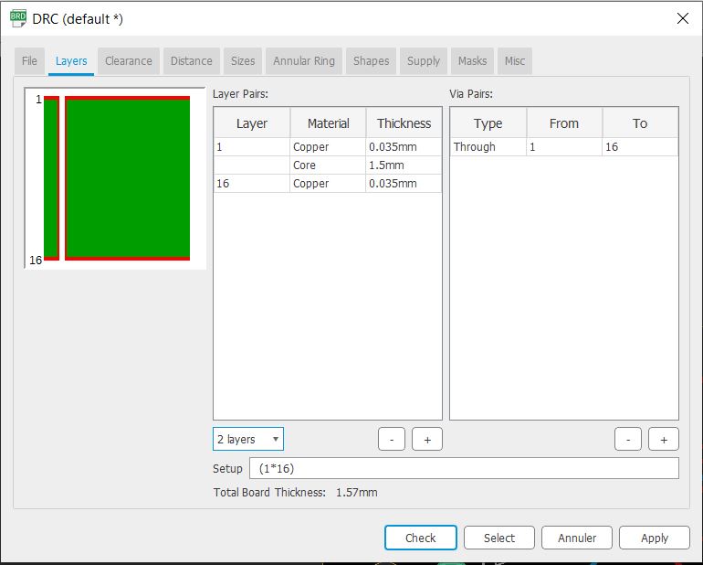
The Layers tab defines which signal layers the board actually uses, how thick the copper and isolation layers are, and what kinds of vias can be placed (note that this applies only to actual vias; so even if no via from layer 1 to 16 has been defined in the layer setup, pads will always be allowed).
The layer setup is defined by the string in the “Setup” field. This string consists of a sequence of layer numbers, separated by one of the characters ‘‘ or ‘+’, where ‘‘ stands for core material (also known as FR4 or something similar) and ‘+’ stands for prepreg (or any other kind of isolation material). The actual core and prepreg sequence has no meaning to EAGLE other than varying the color in the layer display at the top left corner of this tab (the actual multilayer setup always needs to be worked out with the board manufacturer). The vias are defined by enclosing a sequence of layers with (…). So the setup string
(1*16)
would mean a two layer board, using layers 1 and 16 and vias going through the entire board (this is also the default value). When building a multilayer board the setup could be something like
((12)+(1516))
which is a four layer board with layer pairs 1/2 and 15/16 built on core material and vias drilled through them, and finally the two layer pairs pressed together with prepreg between them, and vias drilled all the way through the entire board. Besides vias that go trough an entire layer stack (which are commonly referred to as buried vias in case they have no connection to the Top and Bottom layer) there can also be vias that are not drilled all the way through a layer stack, but rather end at a layer inside that stack. Such vias are known as blind vias and are defined in the “Setup” string by enclosing a sequence of layers with [t:…:b], where t and b are the layers up to which that via will go from the top or bottom side, respectively. A possible setup with blind vias could be
[2:1+((23)+(1415))+16:15]
which is basically the previous example, with two additional outer layers that are connected to the next inner layers by blind vias. It is also possible to have only one of the t or b parameters, so for instance
[2:1+((23)+(1516))]
would also be a valid setup. Finally, blind vias are not limited to starting at the Top or Bottom layer, but may also be used in inner layer stacks, as in
[2:1+[3:2+(3*4)+5:4]+16:5]
A blind via from layer a to layer b also implements all possible blind vias from layer a to all layers between layers a and b, so
[3:1+2+(3*16)]
would allow blind vias from layer 1 to 2 as well as from 1 to 3.
Clearance
![]()
The Clearance tab defines the various minimum clearance values between objects in signal layers. These are usually absolute minimum values that are defined by the production process used and should be obtained from your board manufacturer. The actual minimum clearance between objects that belong to different signals will also be influenced by the net classes the two signals belong to.
Note that a polygon in the special signal named OUTLINES will be used to generate outlines data and as such will not adhere to these clearance values.
Distance
The Distance tab defines the minimum distance between objects in signal layers and the board dimensions, as well as that between any two drill holes. Note that only signals that are actually connected to at least one pad or smd are checked against the board dimensions. This allows edge markers to be drawn in the signal layer without generating DRC errors.
For compatibility with version 3.5x the following applies: If the minimum distance between copper and dimension is set to 0 objects in the Dimension layer will not be taken into account when calculating polygons (except for Holes, which are always taken into account). This also disables the distance check between copper and dimension objects.
Sizes
The Sizes tab defines the minimum width of any objects in signal layers and the minimum drill diameter. These are usually absolute minimum values that are defined by the production process used and should be obtained from your board manufacturer. The actual minimum width of signal wires and drill diameter of vias will also be influenced by the Net Class the signal belongs to.
Restring
The Restring tab defines the width of the copper ring that has to remain after the pad or via has been drilled. Values are defined in percent of the drill diameter and there can be an absolute minimum and maximum limit. Restrings for pads can be different for the top, bottom and inner layers, while for vias they can be different for the outer and inner layers. If the actual diameter of a pad (as defined in the library) or a via would result in a larger restring, that value will be used in the outer layers. Pads in library packages can have their diameter set to 0, so that the restring will be derived entirely from the drill diameter.
Shapes
The Shapes tab defines the actual shapes for smds and pads. Smds are normally defined as rectangles in the library (with a “roundness” of 0), but if your design requires rounded smds you can specify the roundness factor here. Pads are normally defined as octagons in the library (long octagons where this makes sense), and you can use the combo boxes to specify whether you want to have pads with the same shapes as defined in the library, or always square, round or octagonal. This can be set independently for the top and bottom layer. If the “first” pad of a package has been marked as such in the library it will get the shape as defined in the third combo box (either round, square or octagonal, or no special shape). The Elongation parameters define the appearance of pads with shape Long or Offset.
Supply
The Supply tab defines the dimensions of Thermal and Annulus symbols used in supply layers. Please note that the actual shape of supply symbols may be different when generating output for photoplotters that use specific thermal/annulus apertures! See also the notes about “Supply Layers” in the LAYER command.
Masks
The Masks tab defines the dimensions of solder stop and cream masks. They are given in percent of the smaller dimension of smds, pads and vias and can have an absolute minimum and maximum value. Solder stop masks are generated for smds, pads and those vias that have a drill diameter that exceeds the given Limit parameter. Cream masks are generated for smds only.
Misc
The Misc tab allows you to turn on a grid and angle check.