The assignment goals
This week aims to design and produce something with a digital fabrication process not covered in another assignment, documenting the requirements that your assignment meets, and including everything necessary to reproduce it.
Intaglio PCBs?
Although I am not very skilled at fabricating electronics I am curious about exploring new and faster methods of fabrication. My idea is to test an approach similar to intaglio), a traditional printmaking method to craft a working PCB.
](https://cdn-images-1.medium.com/max/2000/1*dOjIeBFJJ3blgxmurpvEkw.jpeg)
This blog: 21st-century renaissance print maker explains the classic intaglio process in detail.
Adapting intaglio to PCB fabrication means carving the PCB material traces and then filling them with conductive ink, later, placing the SMD components with the same conductive ink to fix them.
This will allow for rapid prototyping of the traces with a common use laser cutter and the possibility of using various materials for the PCB matrix such as acrylic (transparent PCBs maybe?). This also reduces the time of soldering the components.
Although intaglio is intended to transfer the carved design on the matrix to a paper sheet, I will be using the matrix (carved material) as the final PCB, but some sort of traces transfer could be tested, like the opposite of etching.
Materials
PCB: I’ll be using 3mm transparent acrylic as matrix material
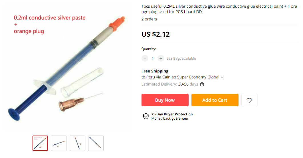
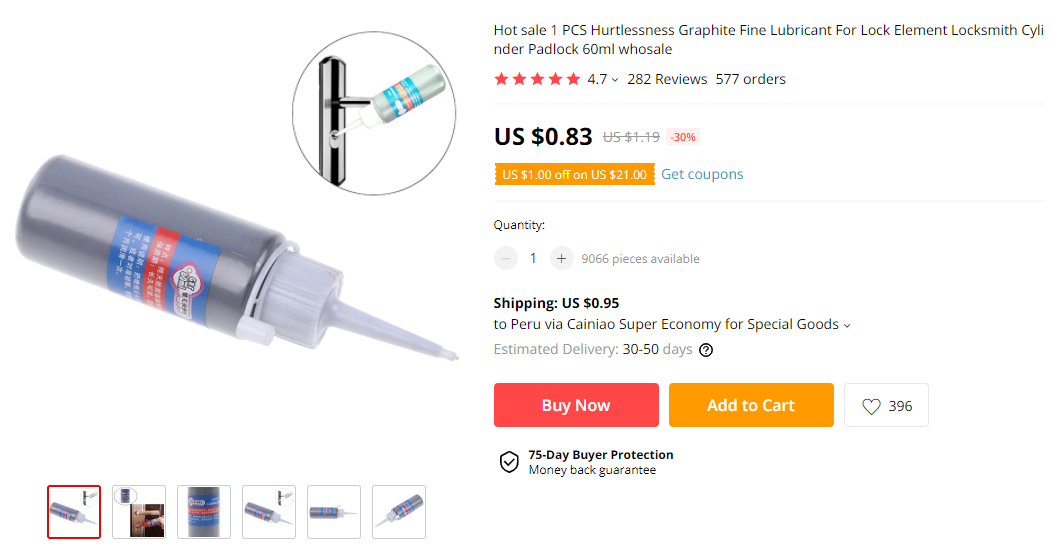
Conductive ink: I ordered conductive silver paste from Aliexpress, which is normally used to repair traces, and powder graphite (lock lubricant?) to make my own conductive ink.
Electronic Components: Various SMD components used in Electronics production and related assignments.
Engraving the traces
The engraving is made with the Trotec Speedy 100 laser cutter, the same used in the Computer-controlled cutting assignment.
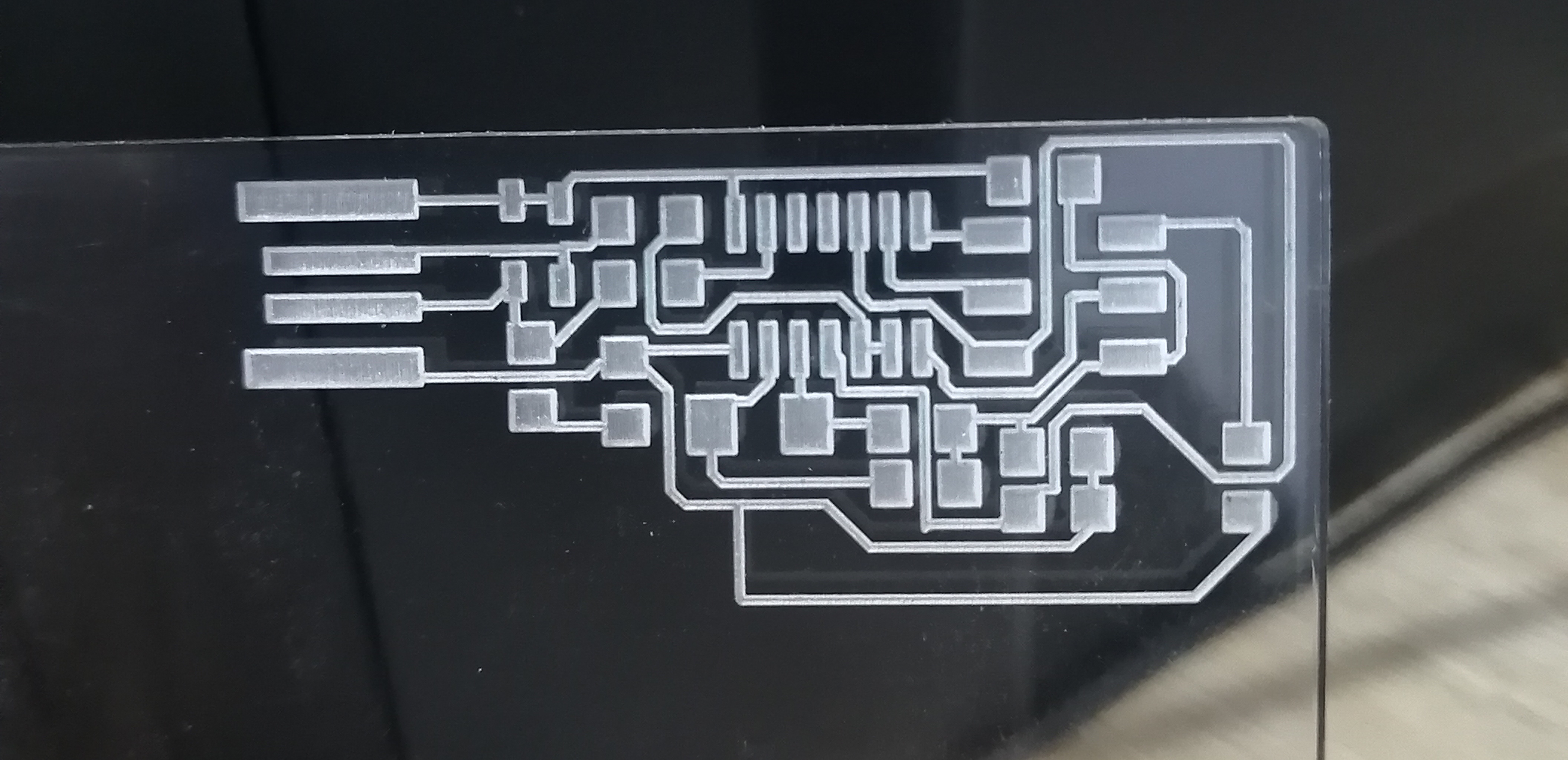
I’ll be testing the engraving process with the Fab ISP design from Valentin Heun because I already made it in the previous assignment.
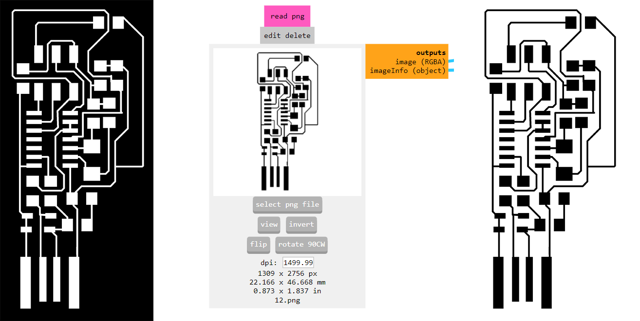
The circuit fabrication files are in .png format, which is fine for PCB fabrication on the model milling machine and can also be used for the laser cutter, but having them in vector format would be better. (more on this later)
The first step is to invert the color, I made it with mods, but any image editing software will do. While working with image (raster) format in the laser engraving, black means full engraving power, we could tweak the values or have different color gradients to indicate the power used. This will cause a deeper or shallow engraving in the matrix.
As this is the first test I’ll be using the default settings for acrylic engraving
It is very important to maintain the image size because these are the real Fab ISP measurements!
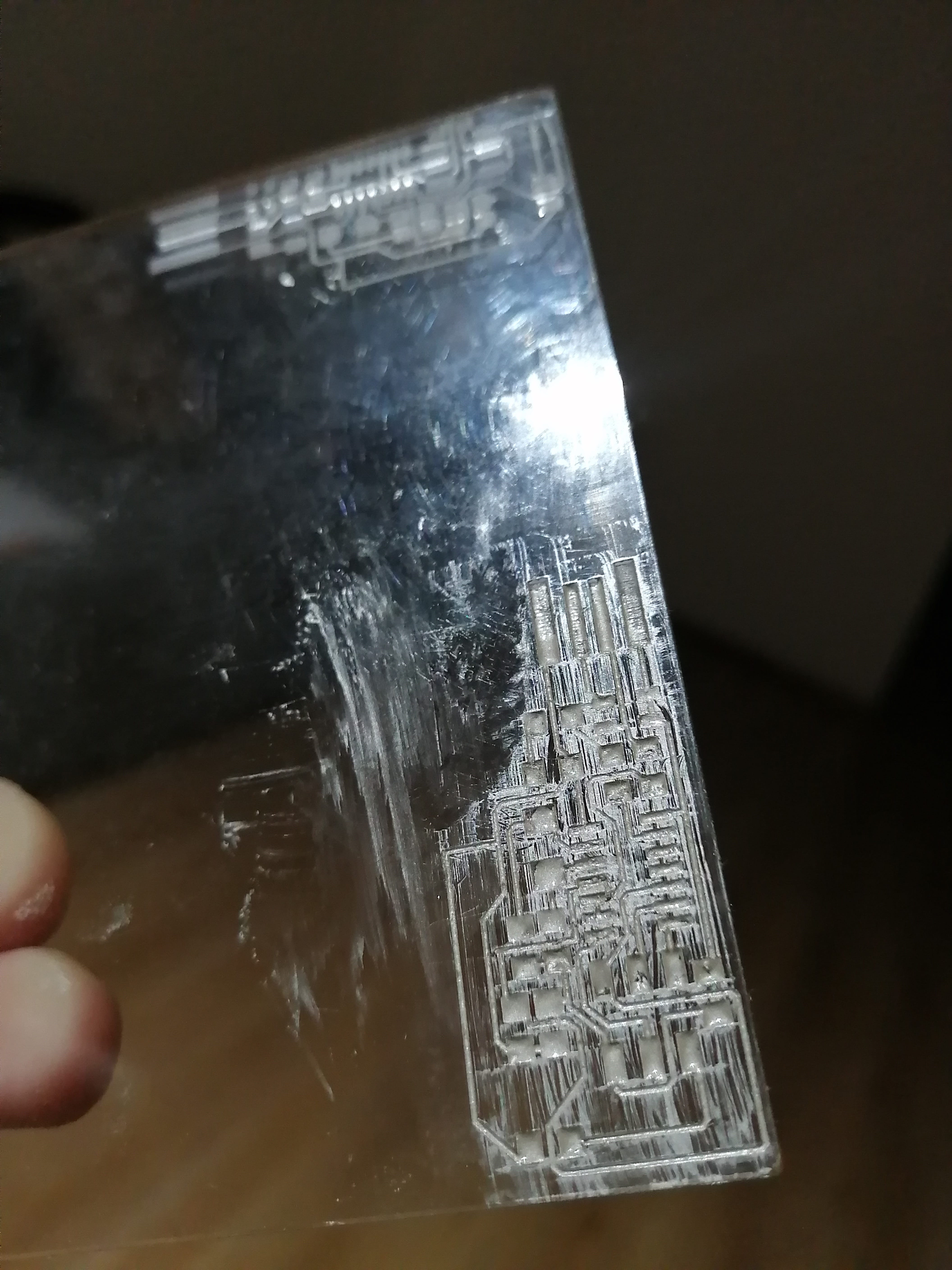
I made this engraving acrylic test to have an idea of how deep the traces would be made, I used a Power 100 / Speed 20 / PPI 1k values to have 0.4mm deep engraved traces.
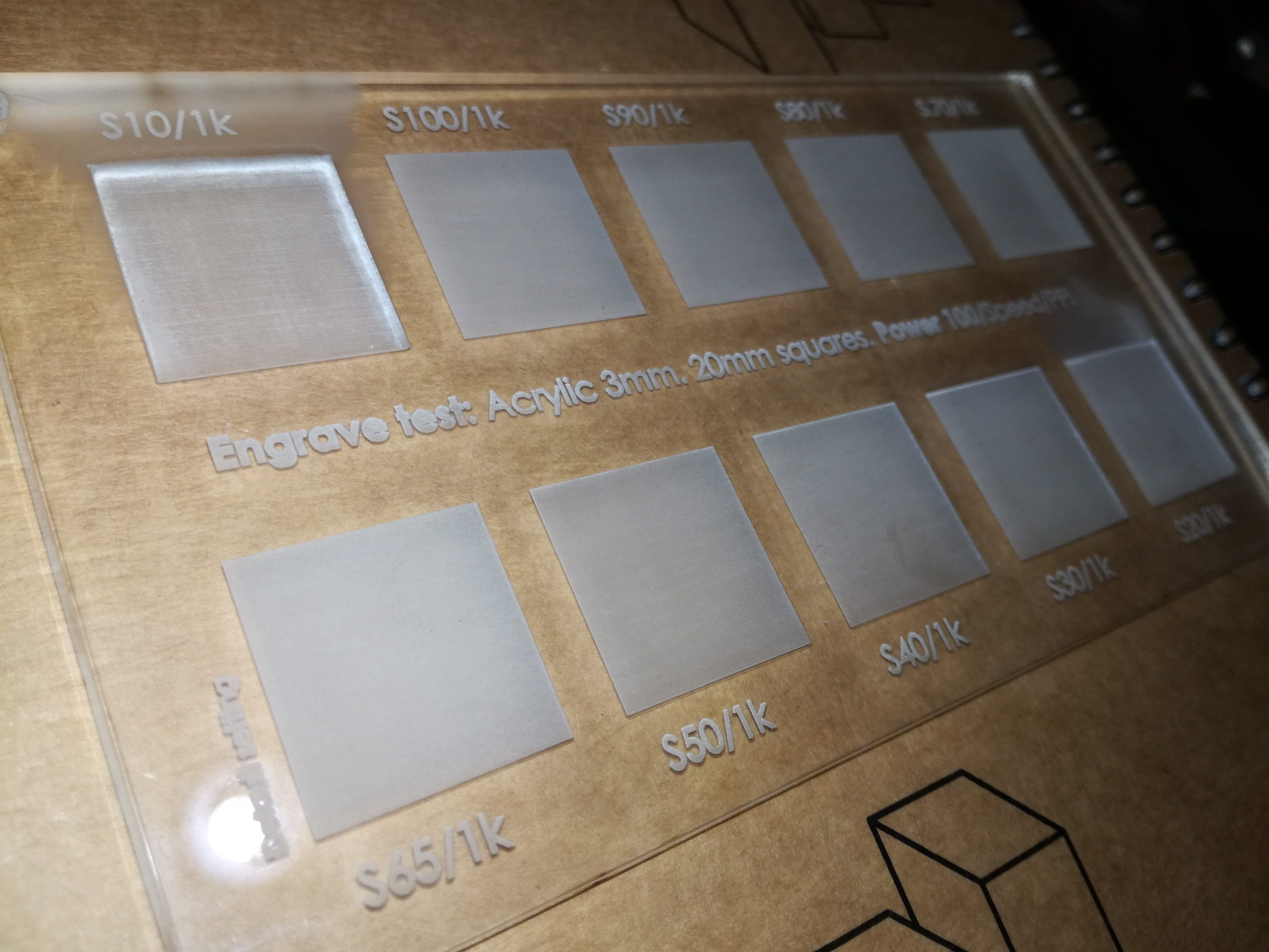
First engraving test! with the settings, the channel depth is approx. 0.4mm
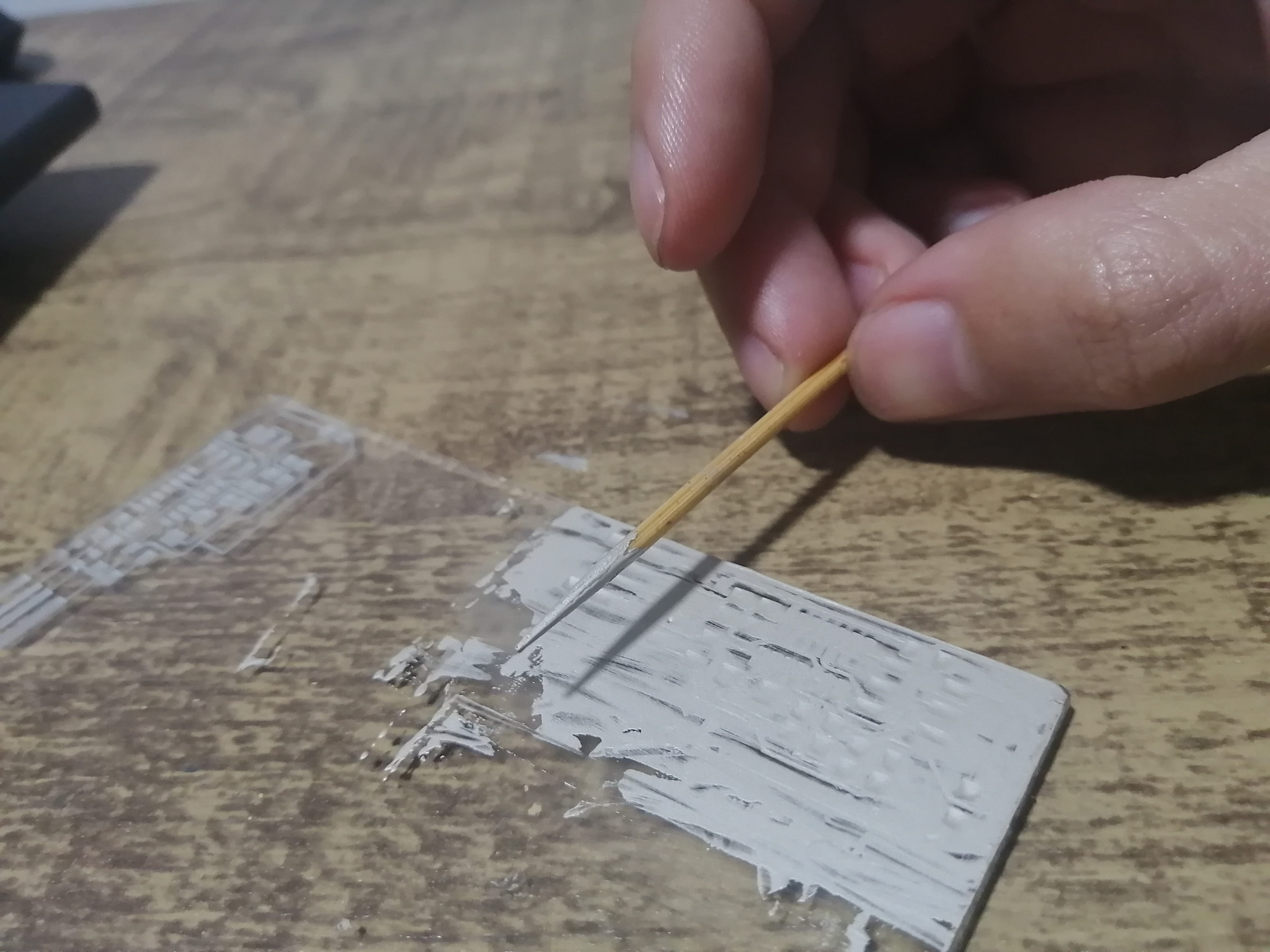
After some cleaning, I noticed that the traces were very thin. My first attempt in filling the traces was with black photocuring resin, this ended up making a bit of a mess but it did go into the engraved traces.
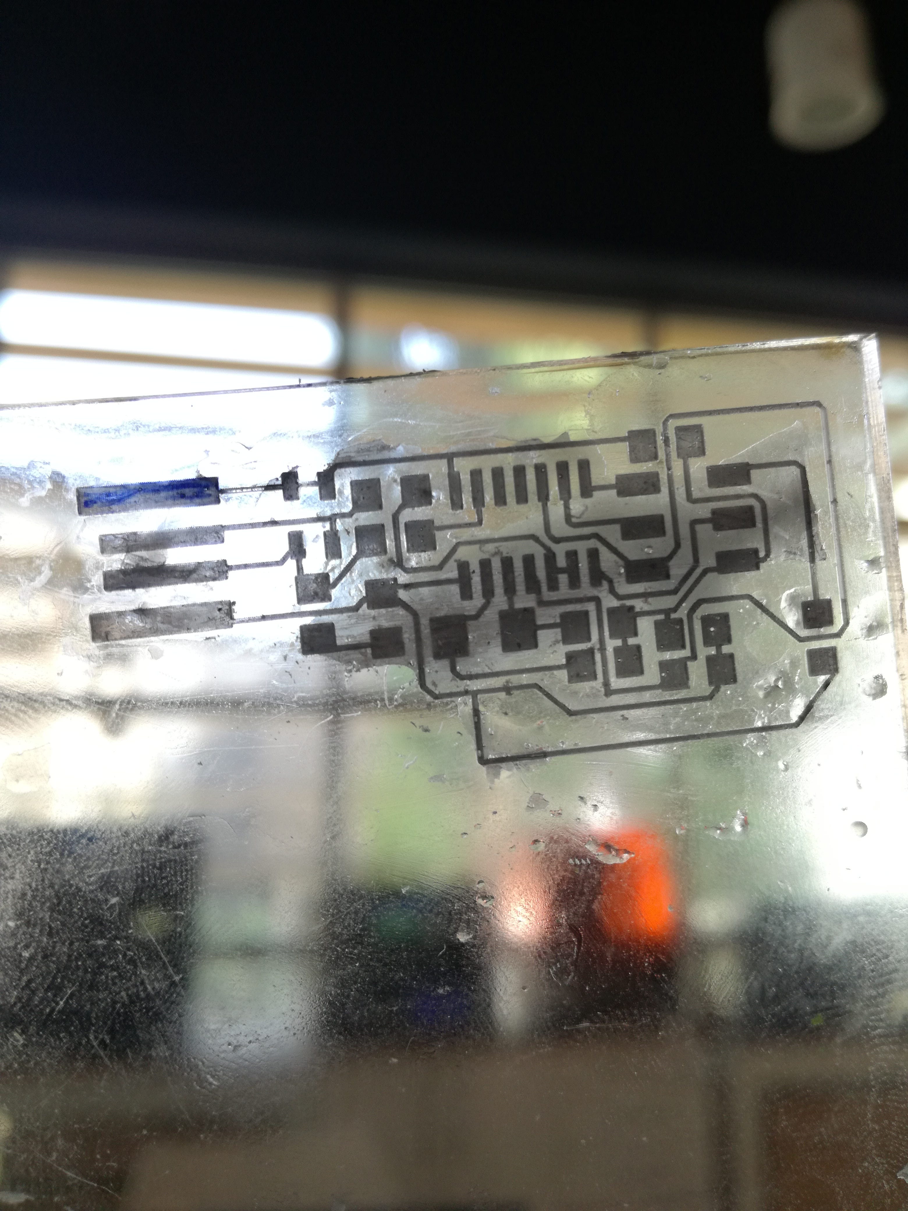
I tried to clean the resin by scrapping the excess with a spatula but this didn't work because it cleared out some chunks of the already filled traces and pads. notice that the resin didn't penetrate in some sections of the traces. but overall the concept worked!
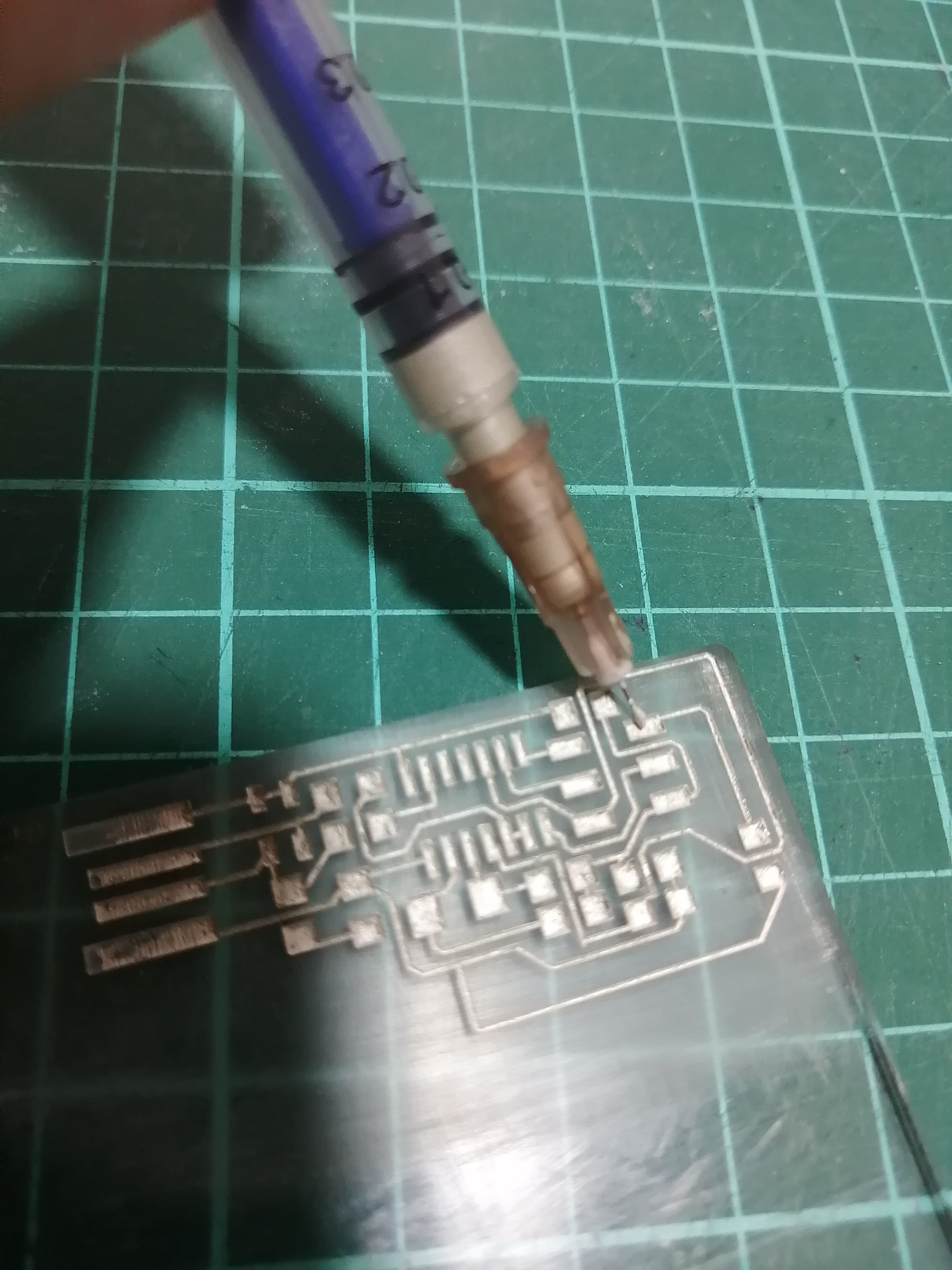
My next test was using the silver conductive paste, I ordered two 0.2ml syringes, It took almost two months to arrive in Peru, and immediately noticed that this is a very little amount of conductive paste!
My first attempt is to use the needle to deposit the paste on the pads, and then spread it to the traces, this proved to be challenging, as the conductive paste has a glue-like consistency and does not easily fill the traces.
I resorted to making little blobs of conductive paste and spread it with the spatula several times until the traces and pads were filling up.
This ended up being quite a mess again! and kind of quickly running out of my first 0.2ml paste (need to order more next time but it's quite expensive!). I let it dry overnight and cleaned it with some light sandpaper.
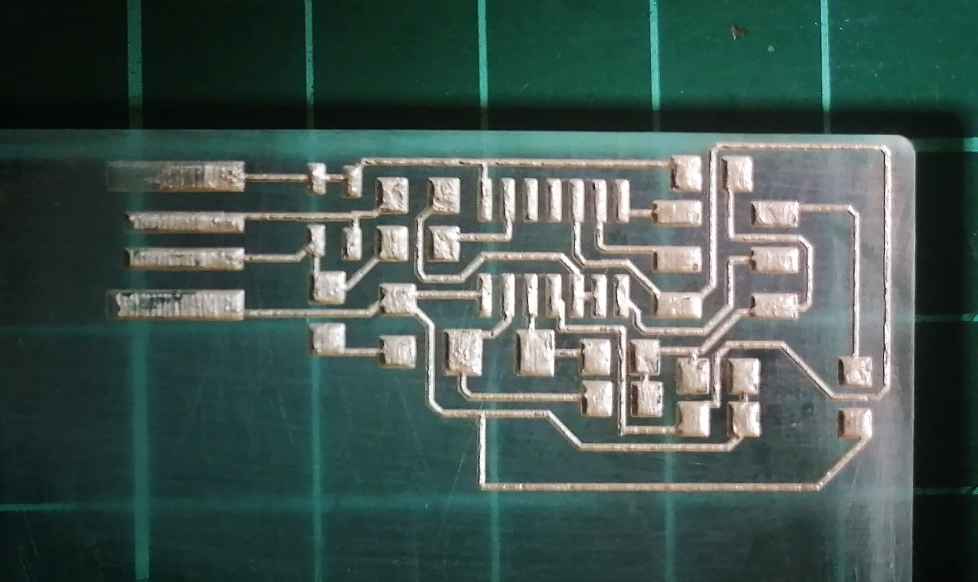
The pads and traces were not filled, even tho the depth of the engraving was only 0.4mm! this was hard to see because of the mess, but the paste also left some unfilled pads that needed a second conductive paste layer.
This second layer covered up the holes but still didn't fill the traces, I guess it only gets to half the depth of the traces, so around 0.2mm or less of conductive paste. This may be more than enough to check conductivity, but I'm worried that some components that lay flat will not be able to touch the conductive paint.
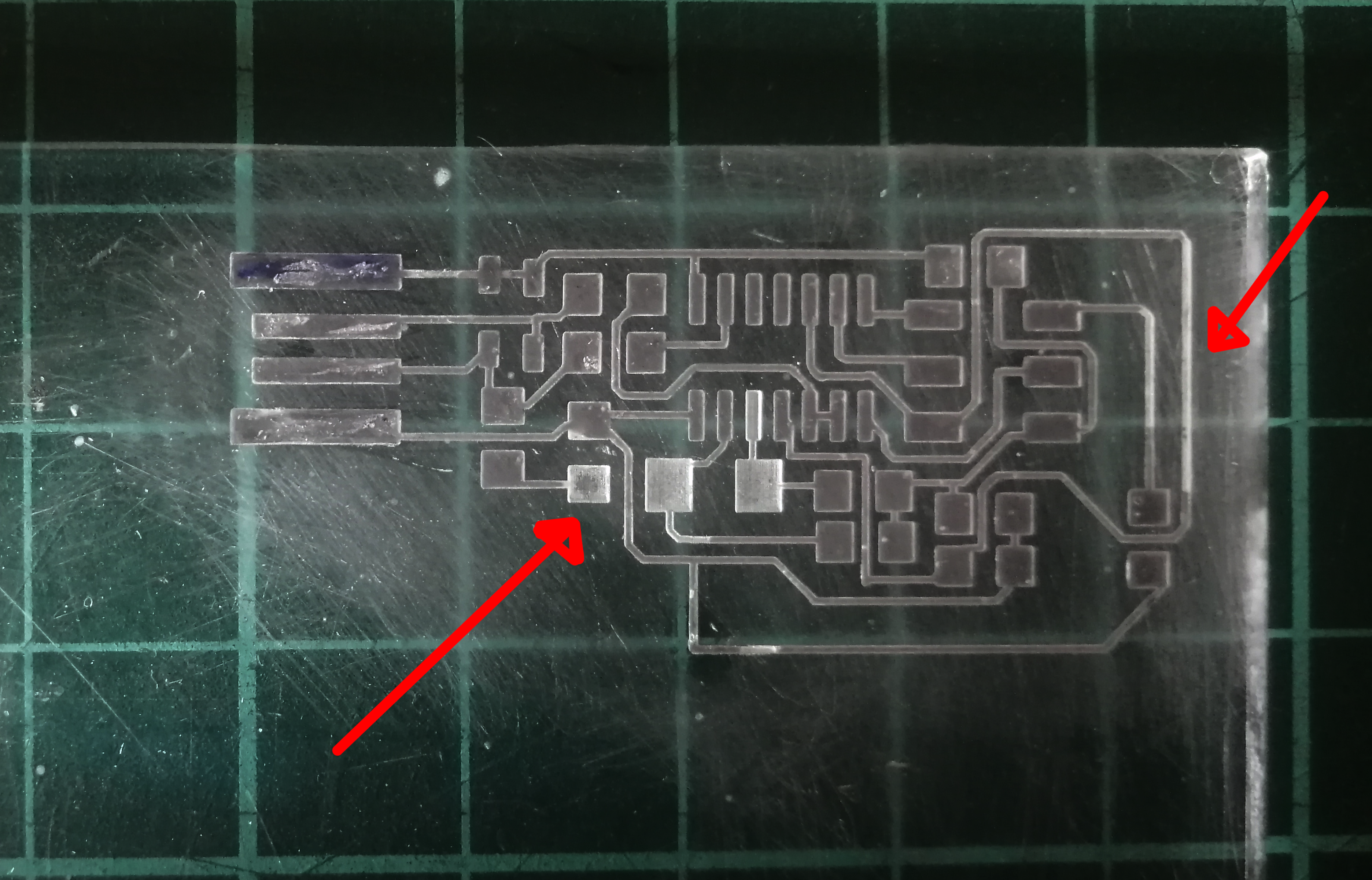
I did not fill up the USB pads because I felt like it would be wasting conductive paste and this was intended only like a conductive test, so not really connecting the ISP to anything.
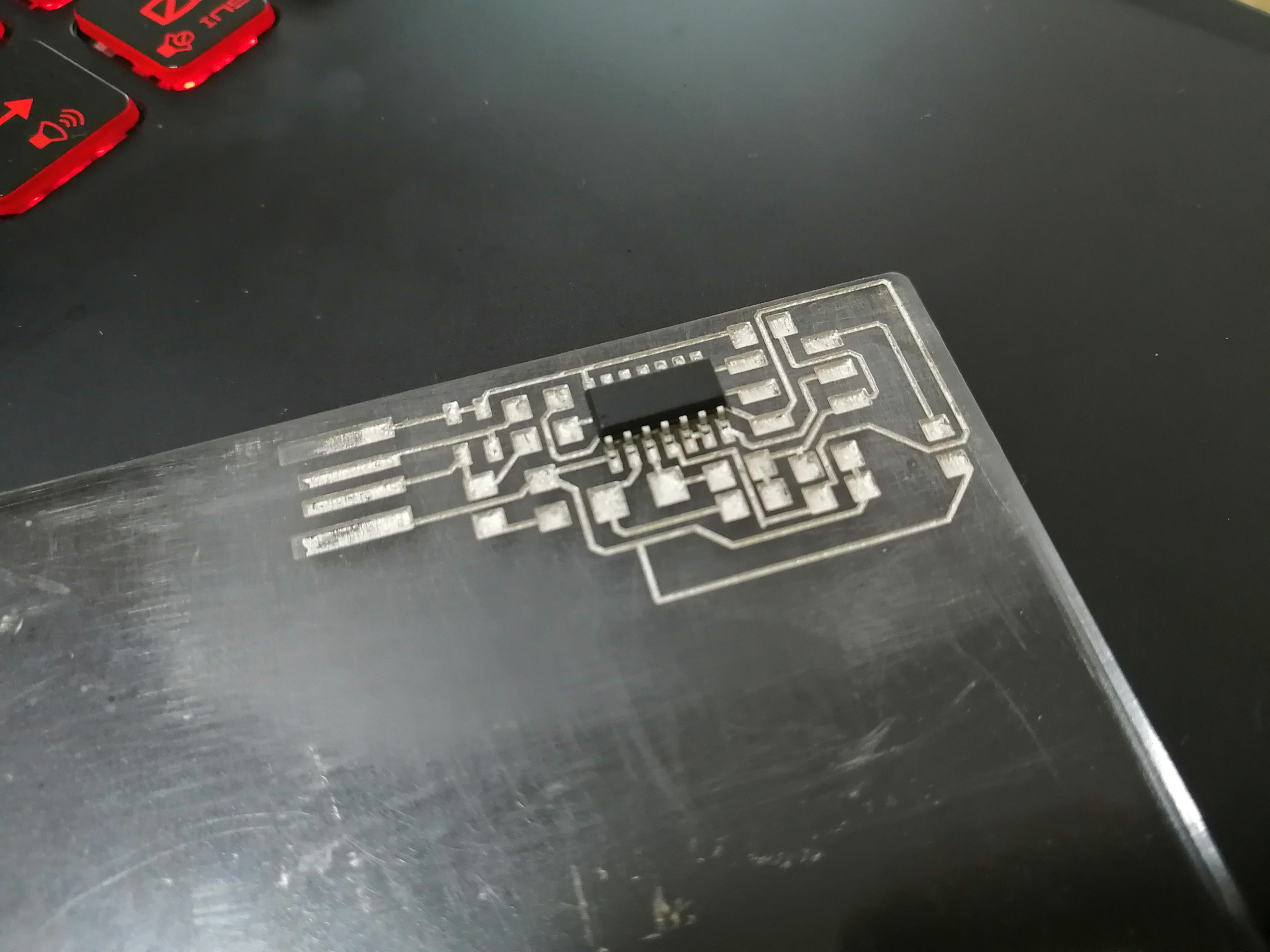
The Attiny44 in its position, the little feet of the microcontroller do touch the conductive paste, the carving also helps to fix it!
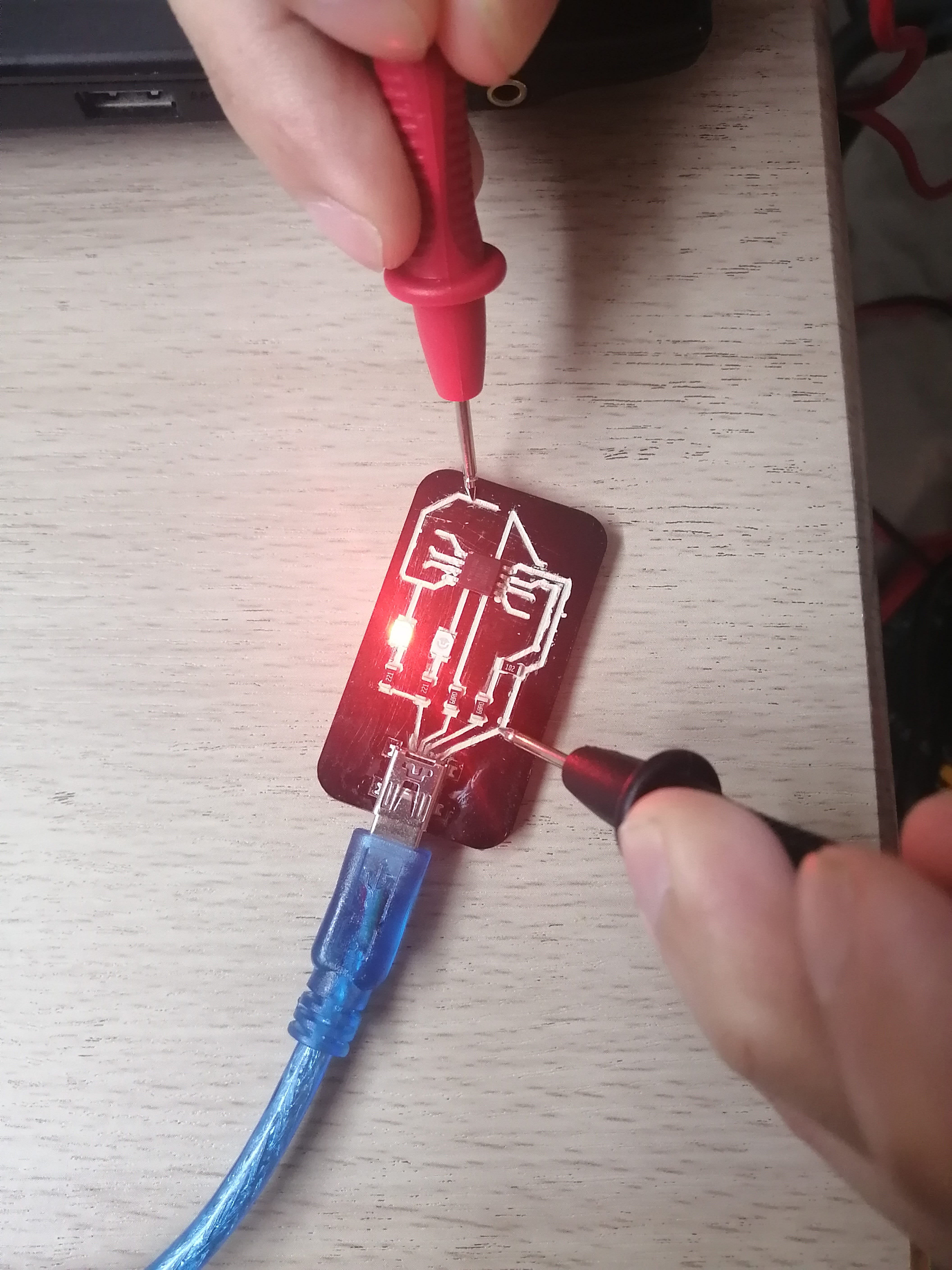
Checking continuity/conductivity
Next, I tested the circuit continuity with a multimeter, The test shown that there is continuity in all the traces and pads, but there’s an important electrical resistance factor.
This resistance goes from around 0.8 to more than 12 ohms depending on how far are the points touched. To get an idea of how good or bad this was, I checked with old copper circuits (made with the vinyl cutter). The resistance found in copper is around 0.4 ohms.
I was surprised because I thought that this silver conductive paste would be a very good conductor, but this resistance might be in part my fault because of the messy filling of the traces, maybe some got contaminated, maybe there is not enough conductive paste in the traces, etc. Also, I was having different resistance values, some significantly better than others in parts that were closer together. More testing is needed.
An important note is that as the paste gets dried, and the more filled traces are the conductivity improves.
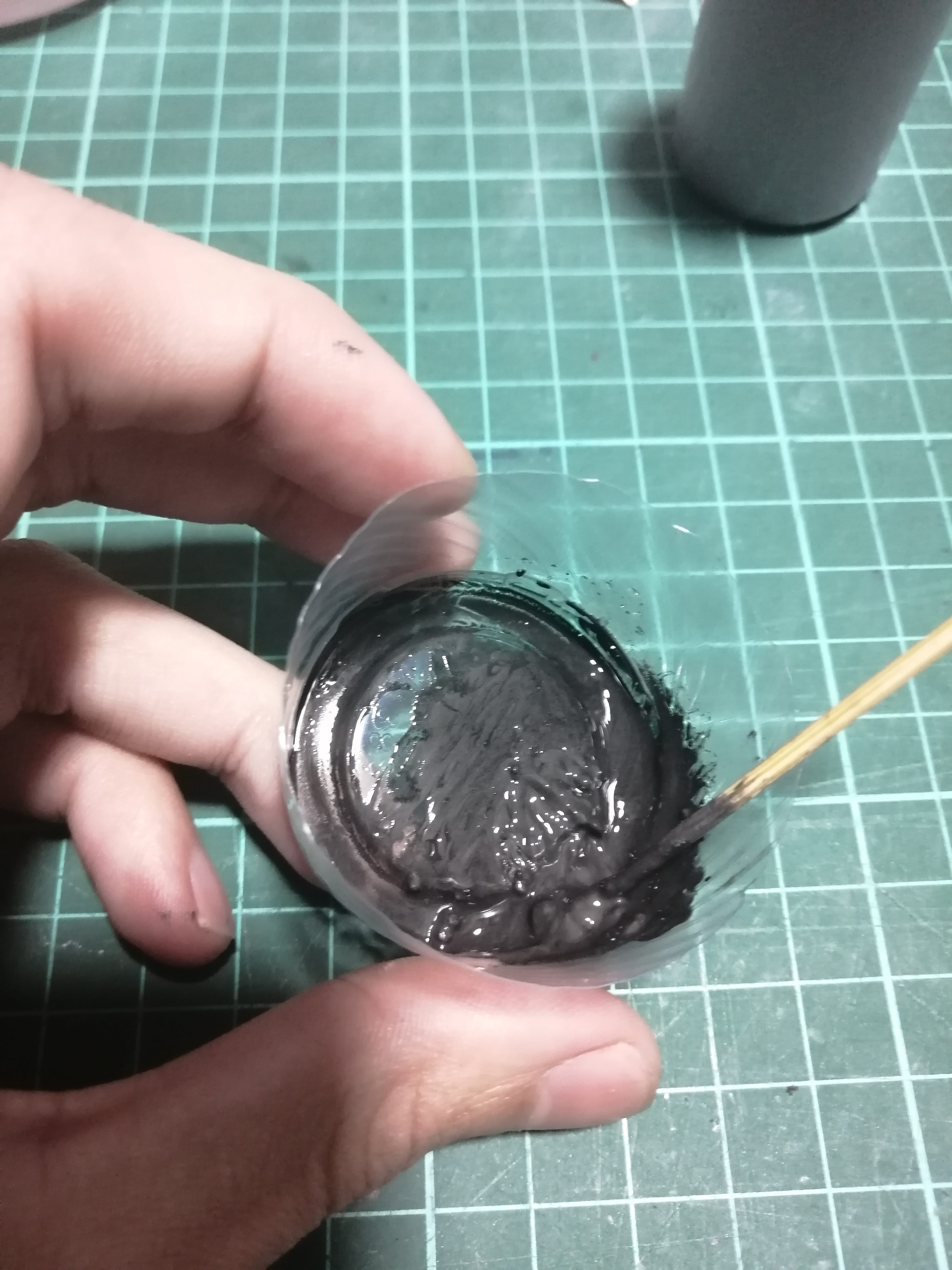
Making conductive paint
For the conductive paint, I'll be using a mix of isopropyl alcohol and graphite powder I ordered from China.
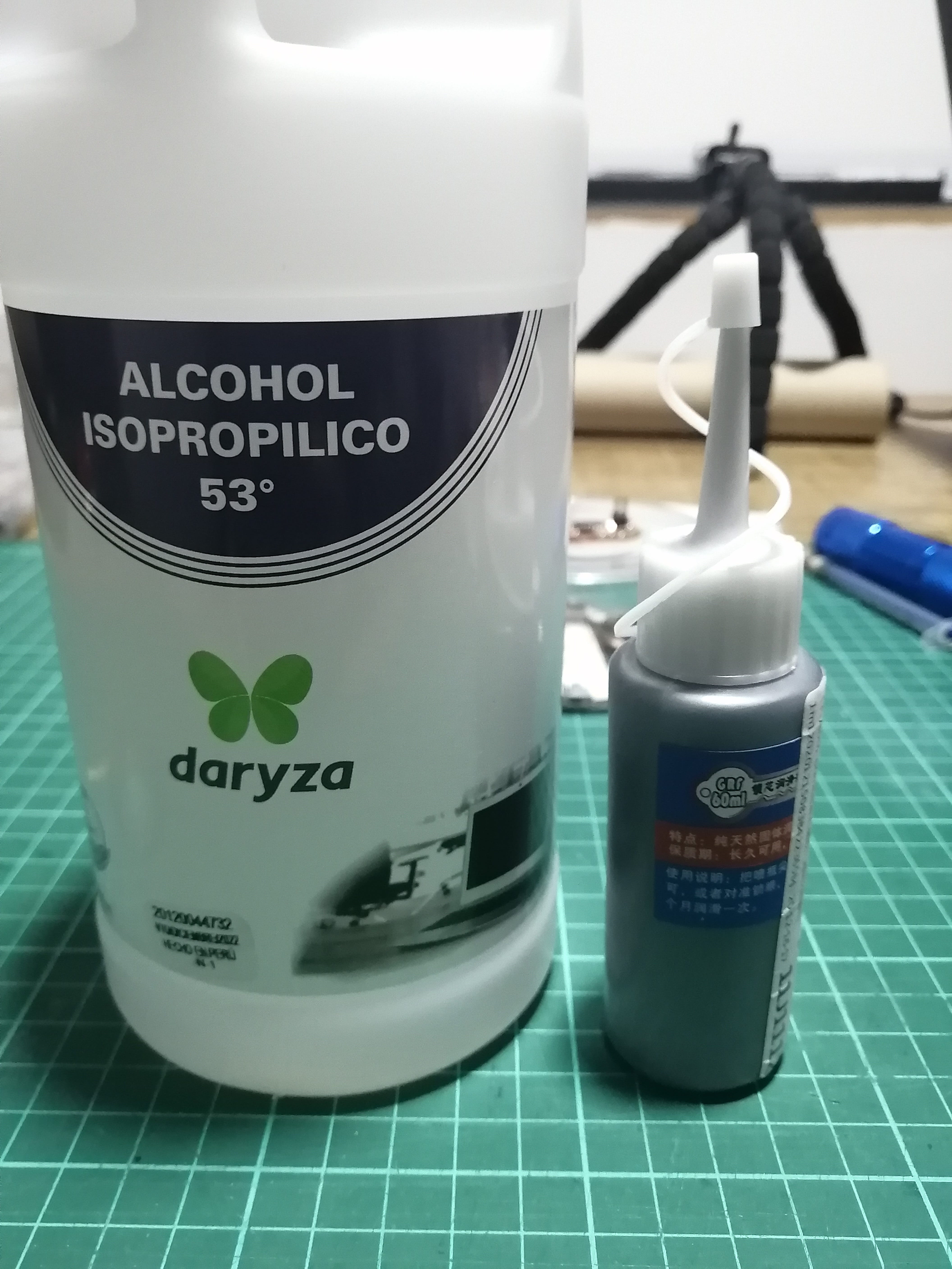
To test this paint I mixed a couple of drops of alcohol and added graphite till it felt like a light paste.
Next, I lay some test strips on cardboard to check resistance.
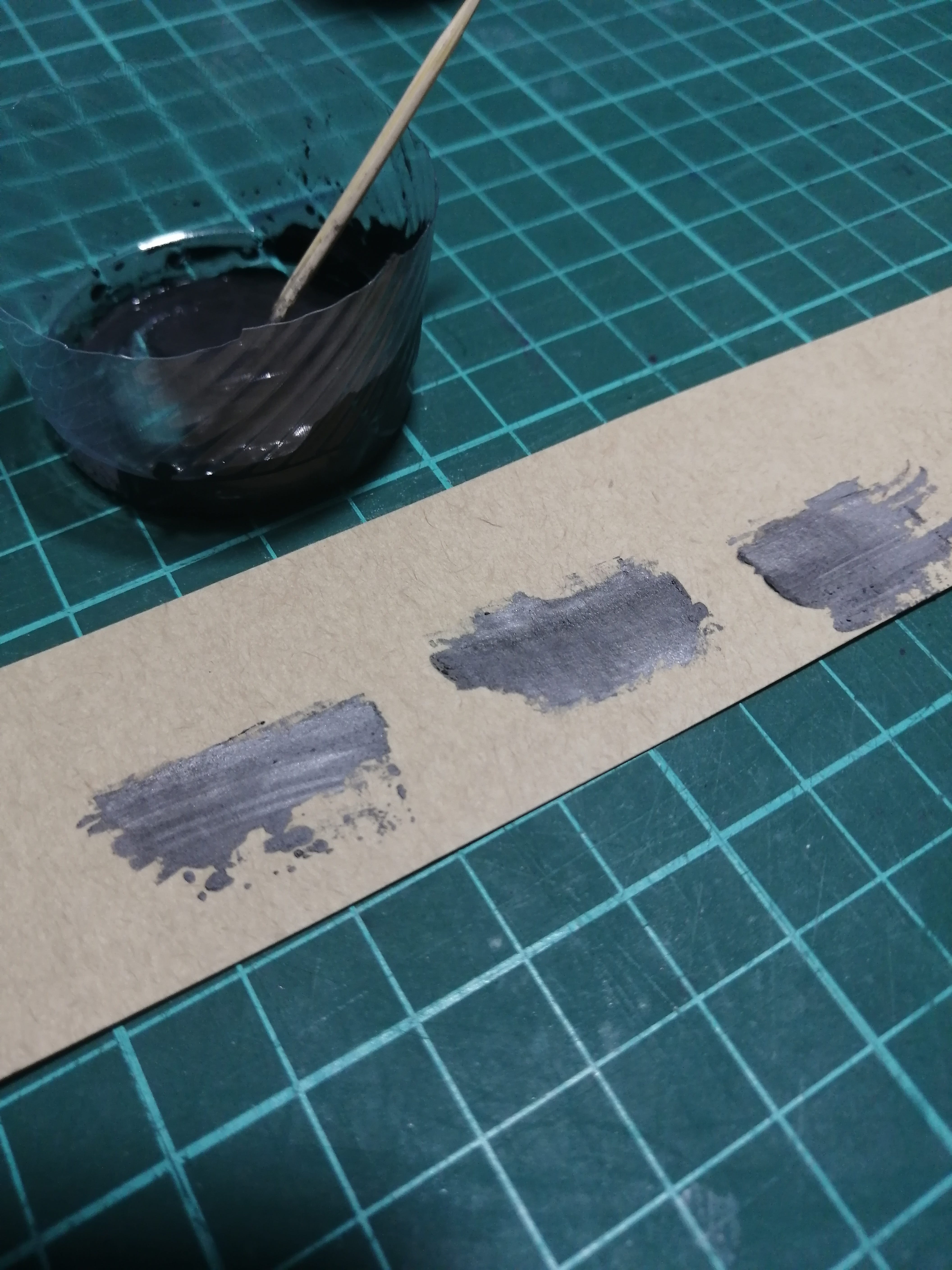
The results were not very good, because of higher than expected resistance values. This improves if the painted layer is thicker, but overall this is not good conductive material. At first, I thought that this might be caused by the isopropyl alcohol because it does not conduct electricity, but I’ve tried a mixture of powder and water and got quite the same results: high resistance.
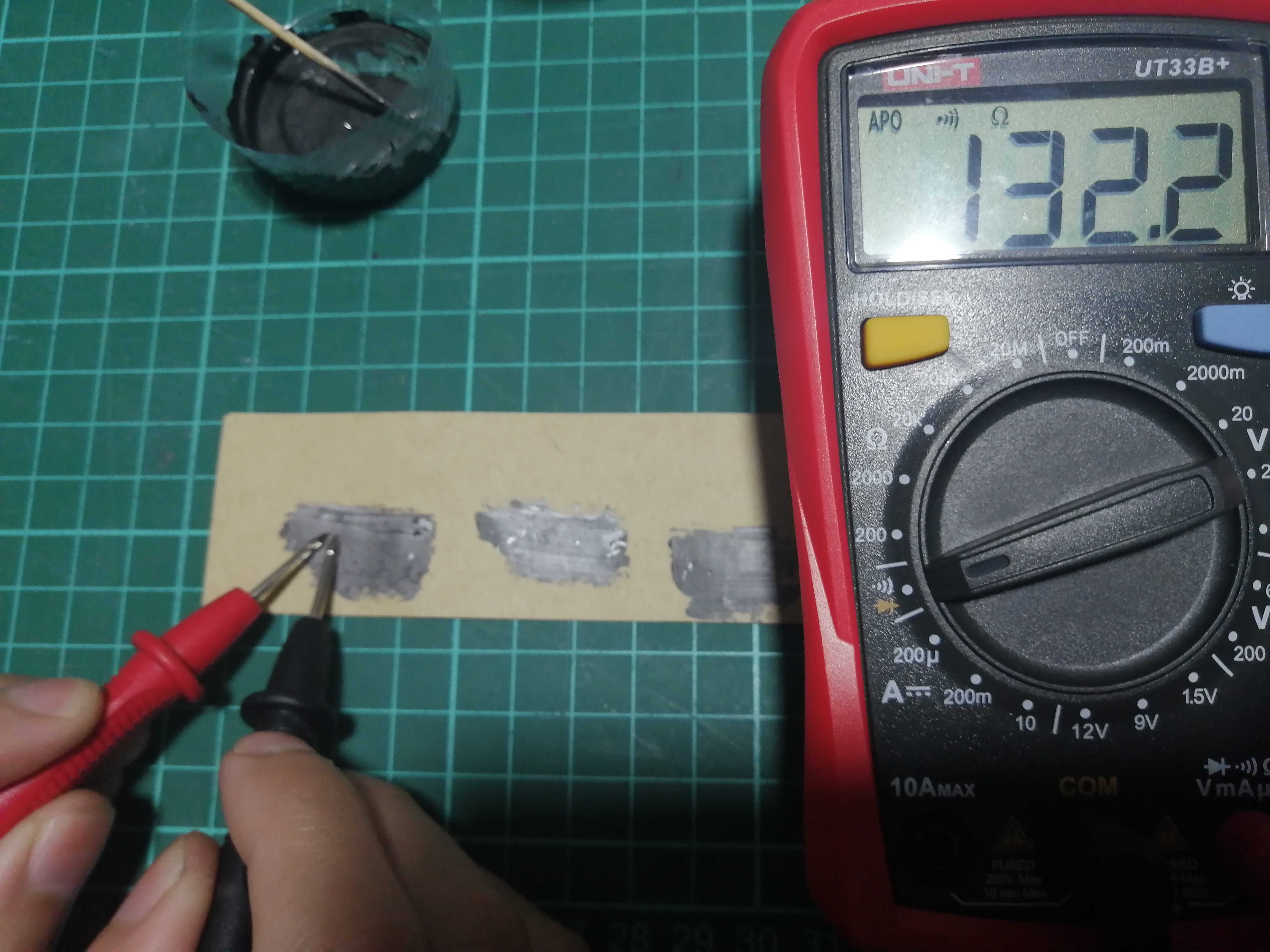
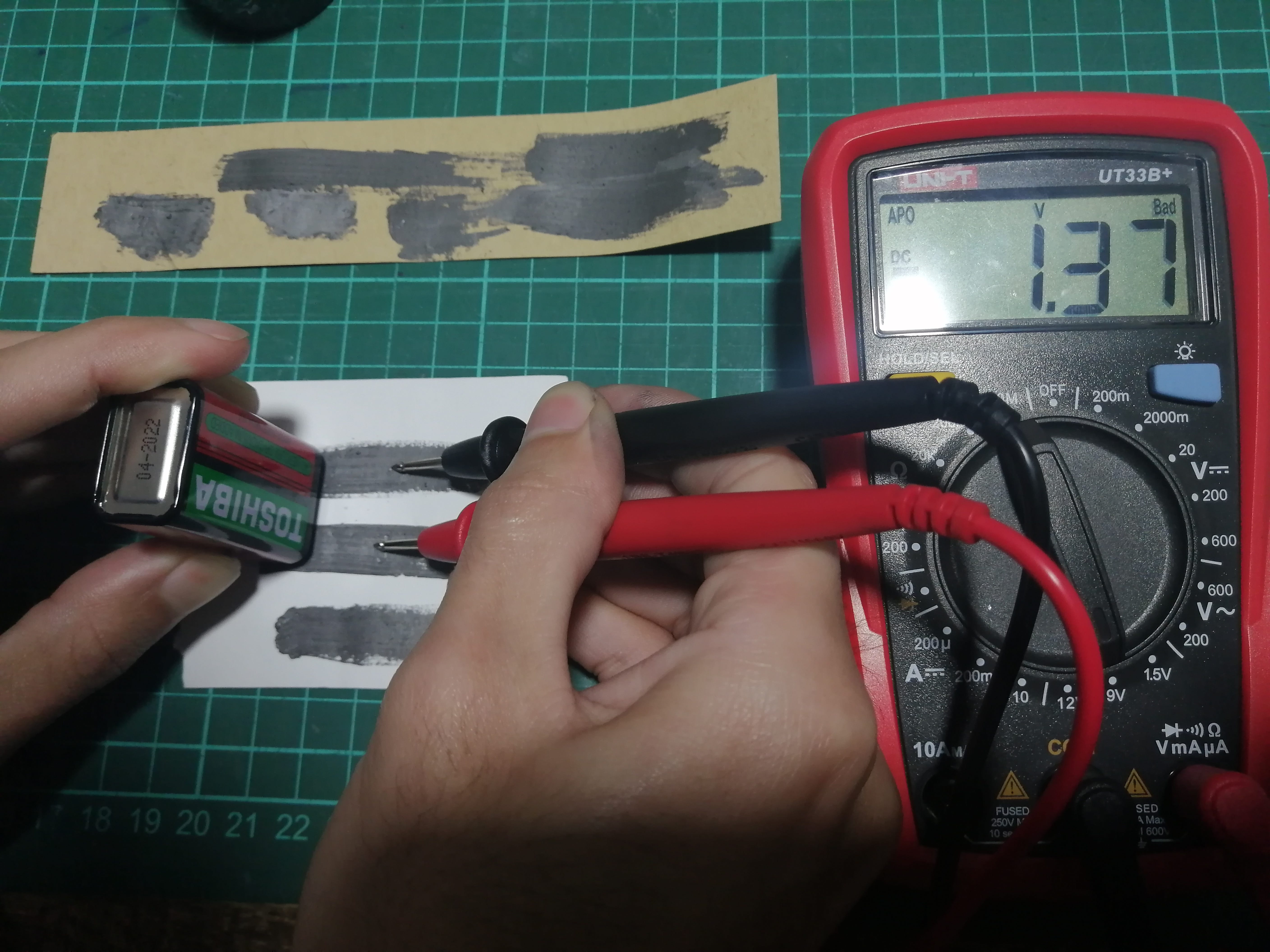
I even submerge the probes in the wet mixture and the dry powder itself but still not conductivity. I also tested two painted traces with a 9v battery. just a couple centimeters apart the voltage from the battery would drop to 1.3v.
Maybe the graphite powder, as it’s intended to be lock lubricant does not work to make conductive paint, I bought it because it was marked as a very fine powder, but I guess better luck next time!
Component placing
As the traces are not completely filled, some of the SMD components did not touch the silver paste. The components that have “legs” that help to bridge this gap could be placed directly. I use to good advantage that the silver paste was not completely dry to push the ATtiny and the 3x2 connector to keep them in place.
To place the other SMD components I added little drops of conductive paste to the conductive pads on the component and on the PCB to fill the gaps. This is like soldering with an iron but much more precise because we are working without worrying about burning! Next, I carefully placed the components with tweezers.
I took out (desoldered) some of the SMD components of another ISP because I didn't have enough stock, and repeated the process.
The process went smooth and uneventful but does require a lot of precision to not make a mess with the paste. I still missing a 499 Ohm resistor to complete the Fab ISP and soldered an LED instead, so this ISP would not be working… although it may be possible to program it.
I would be testing the conductivity again with the components in place, but need to wait almost two days for the paste to completely dry!
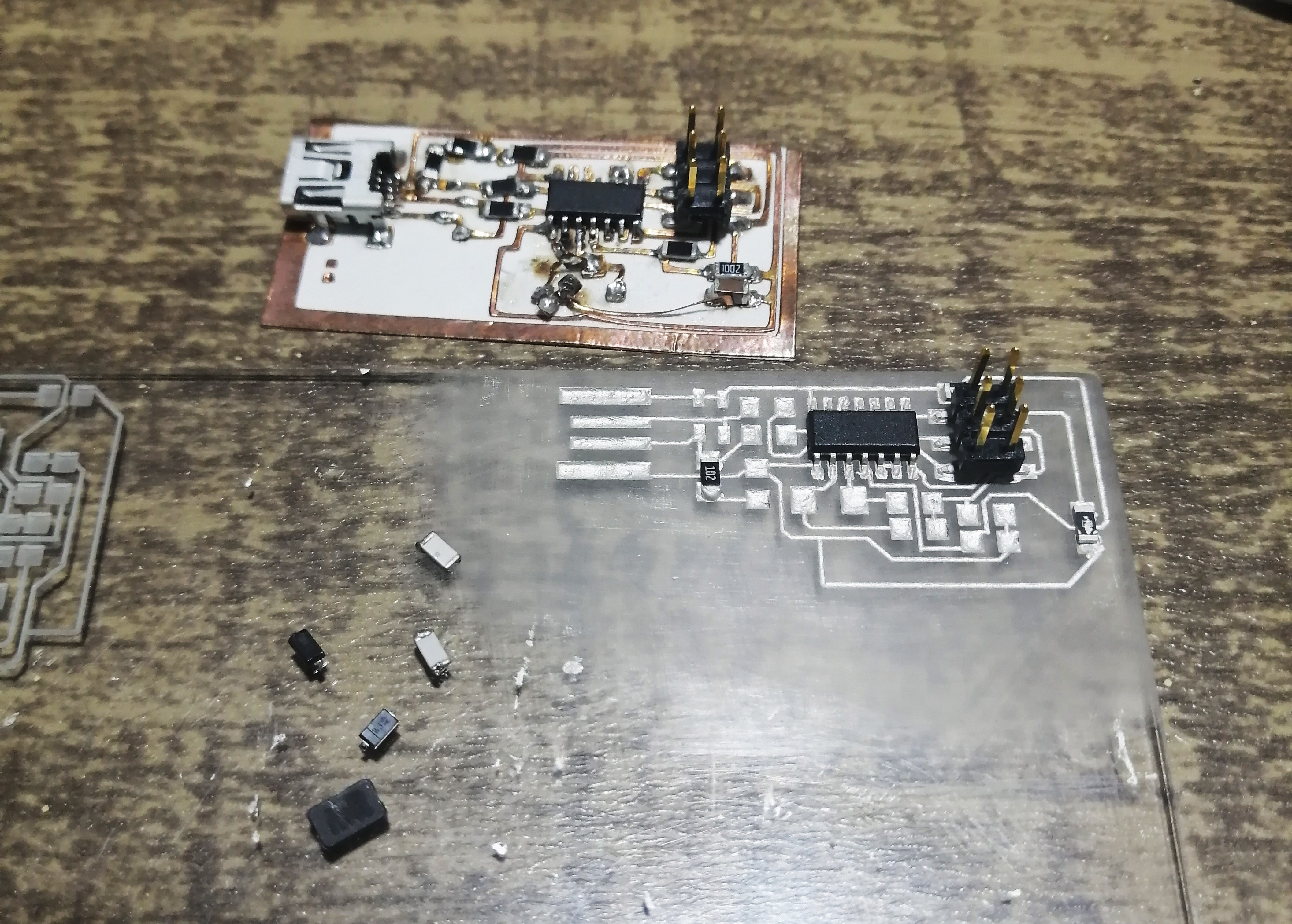
New PCB Design
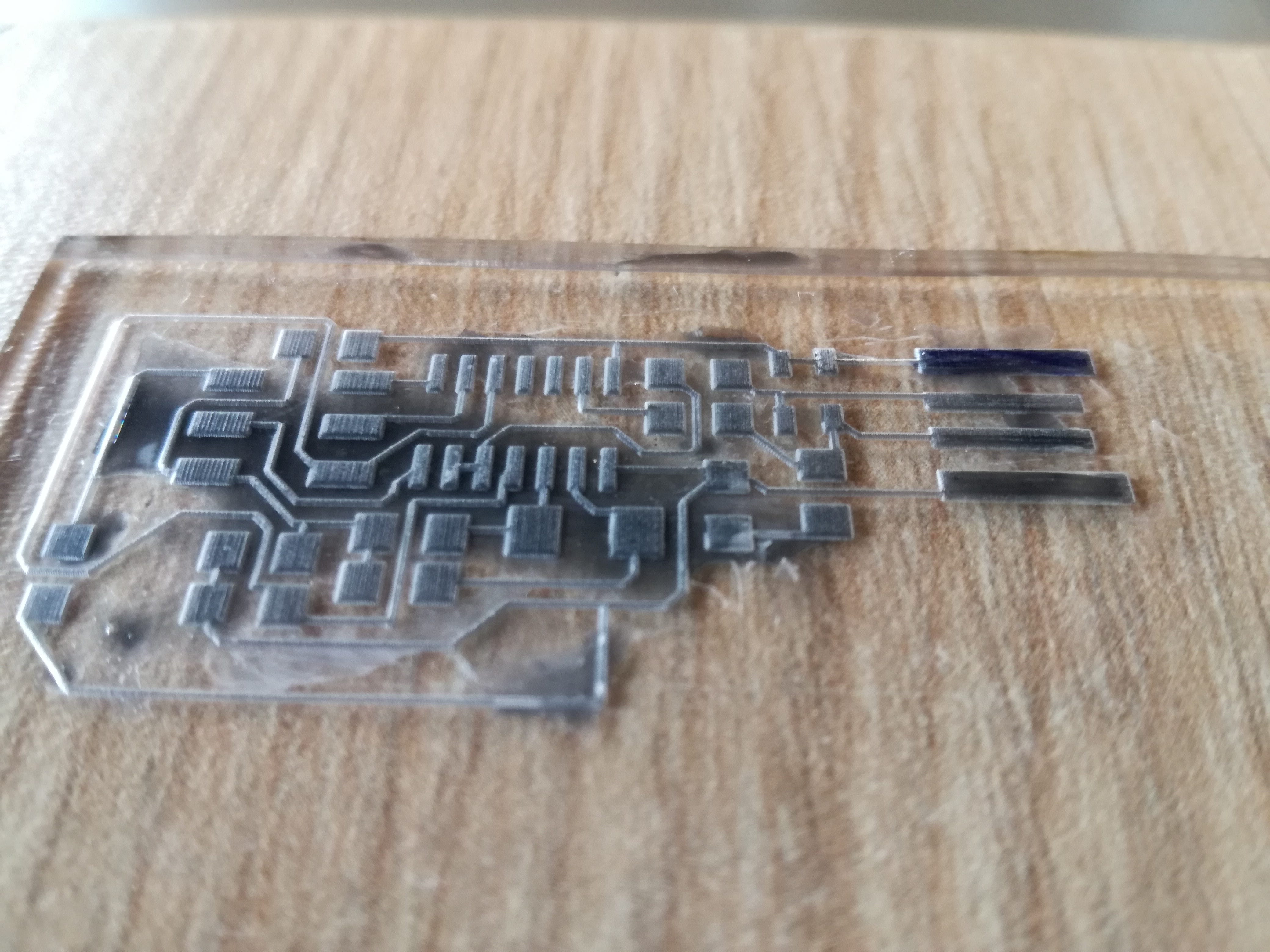
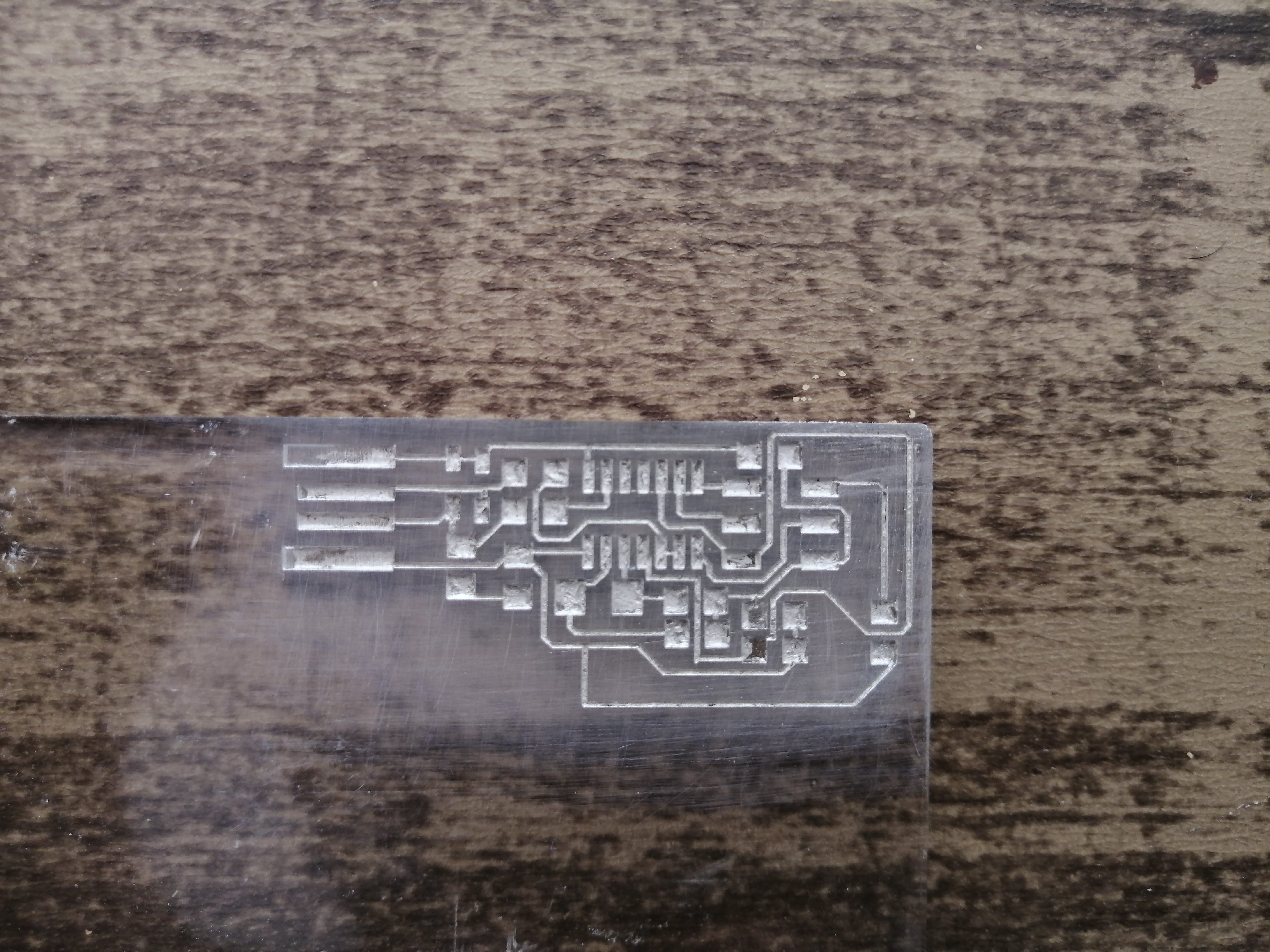
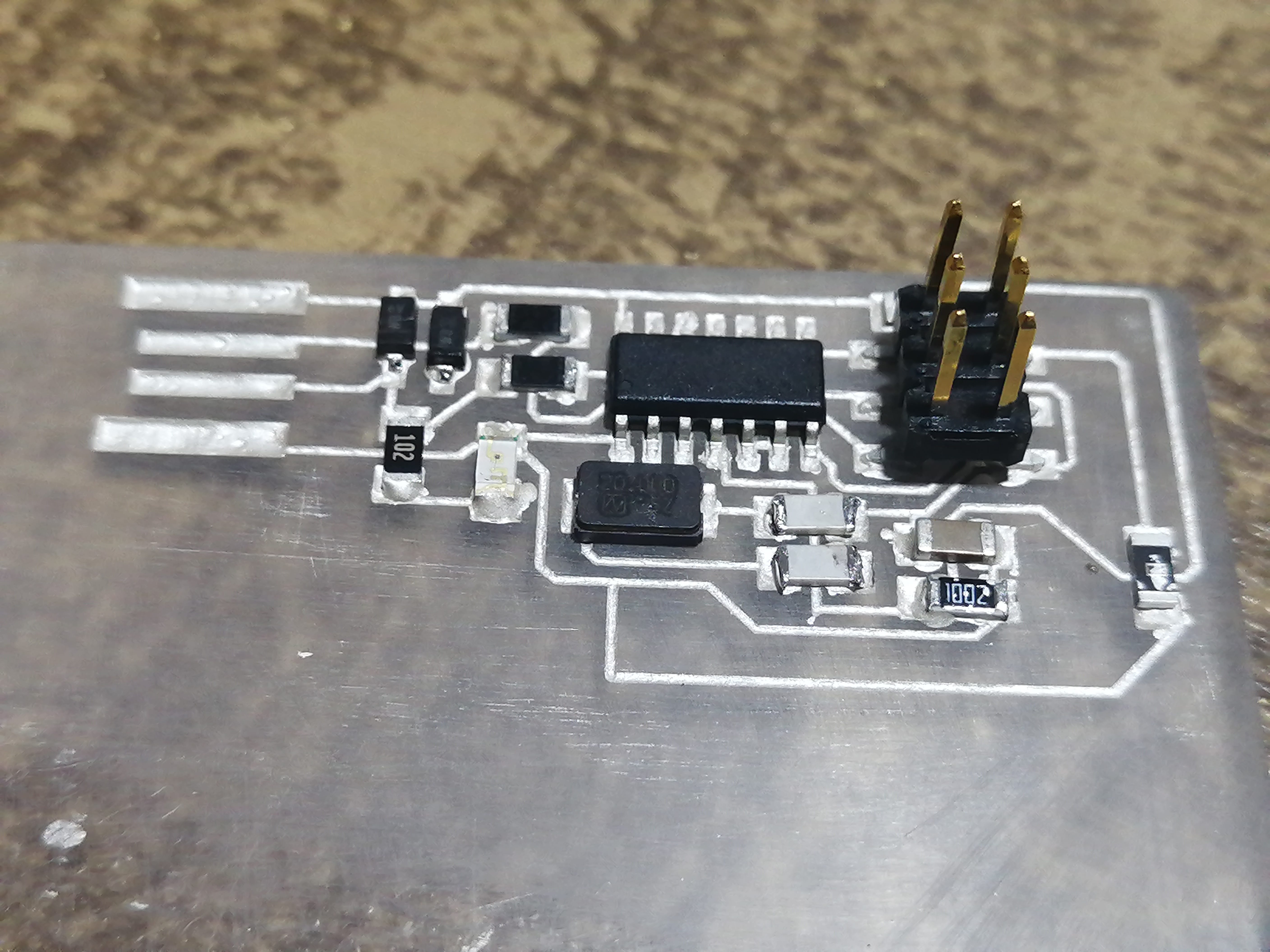
I did a second test with black acrylic and my PCB design, this worked with the Attiny 85. This time I’ll try to make a soldering mask to spread the conductive paste cleaner. I made the mask out of paper although this isn't the best material for a solder mask.
I made this solder mask using the same file as the engraving for the acrylic but generating a cutting vector around the traces. Notice that some tiny gaps in the USB port connection got a bit damaged with the laser.
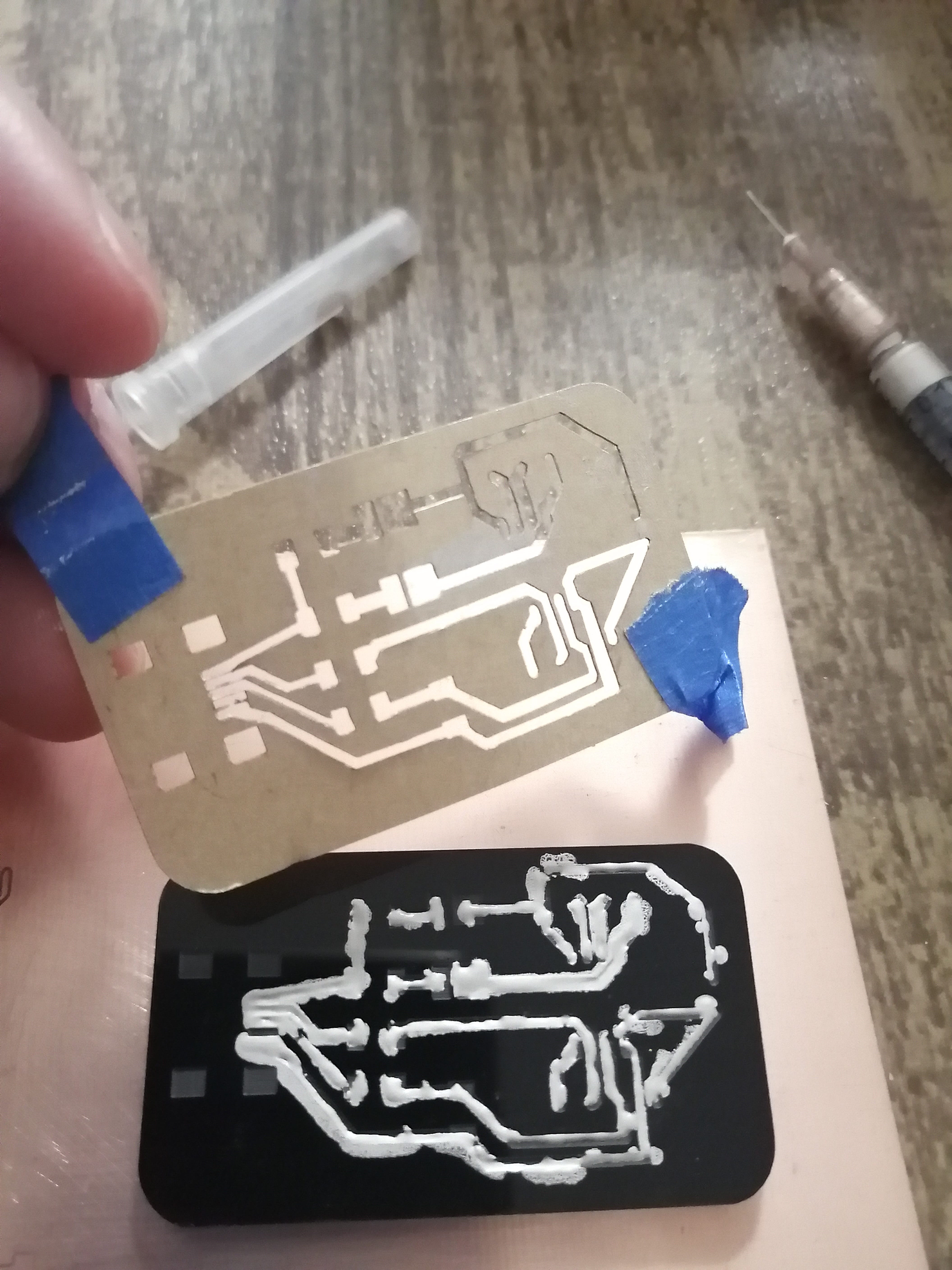
The solder mask didn't go as well as planned but was still better than just spreading the conductive paste directly on the acrylic. some cleaning after was needed.
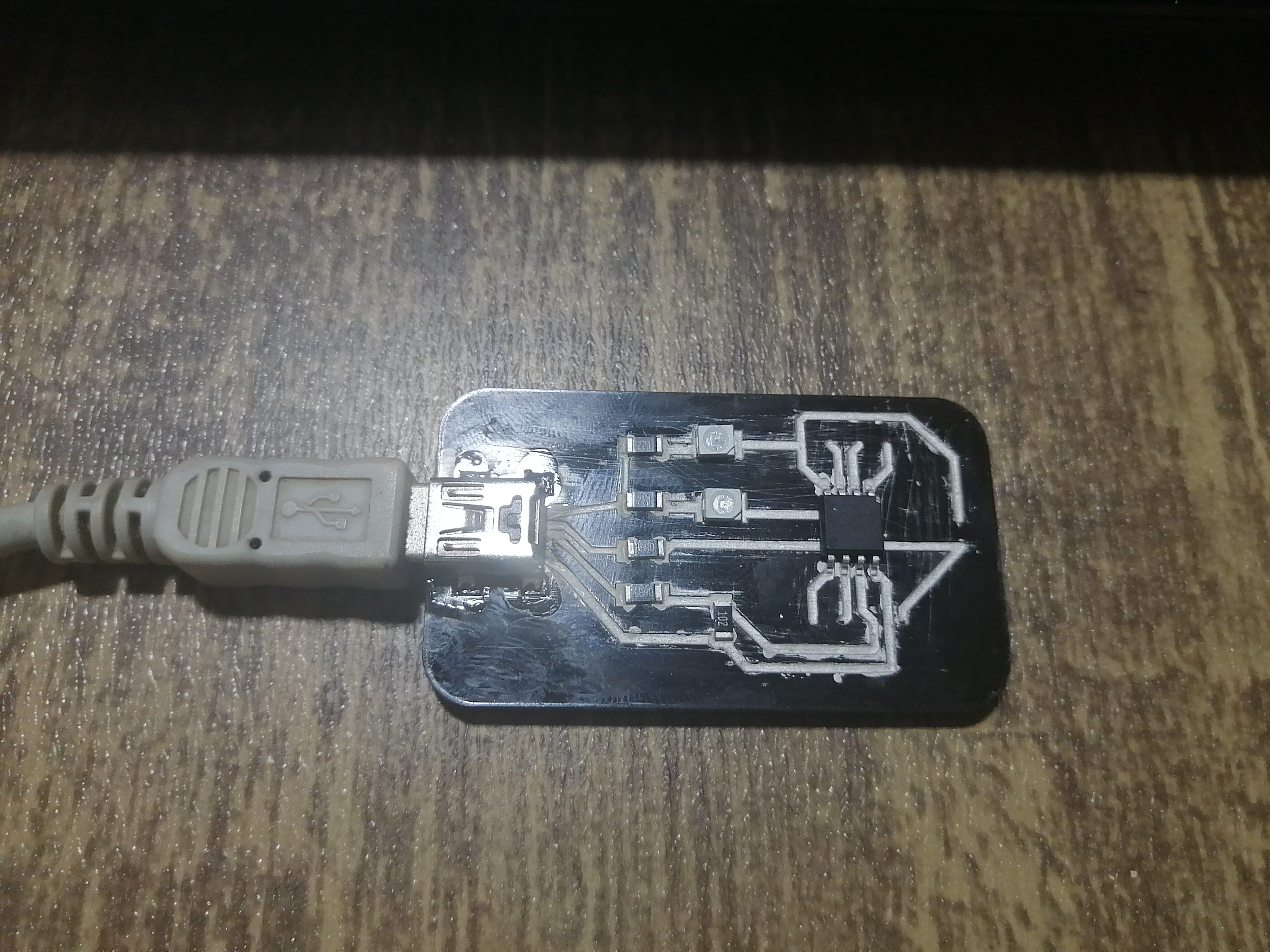
The component placement goes as described before. adding little drops of conductive paste to the conductive pads on the component and on the PCB to fill the gaps.
All the components work as intended this means, correct continuity, correct resistance values, and the LEDs blink!, but as I couldn't place the pins for programming, this PCB wasn't programable.
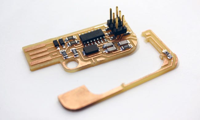
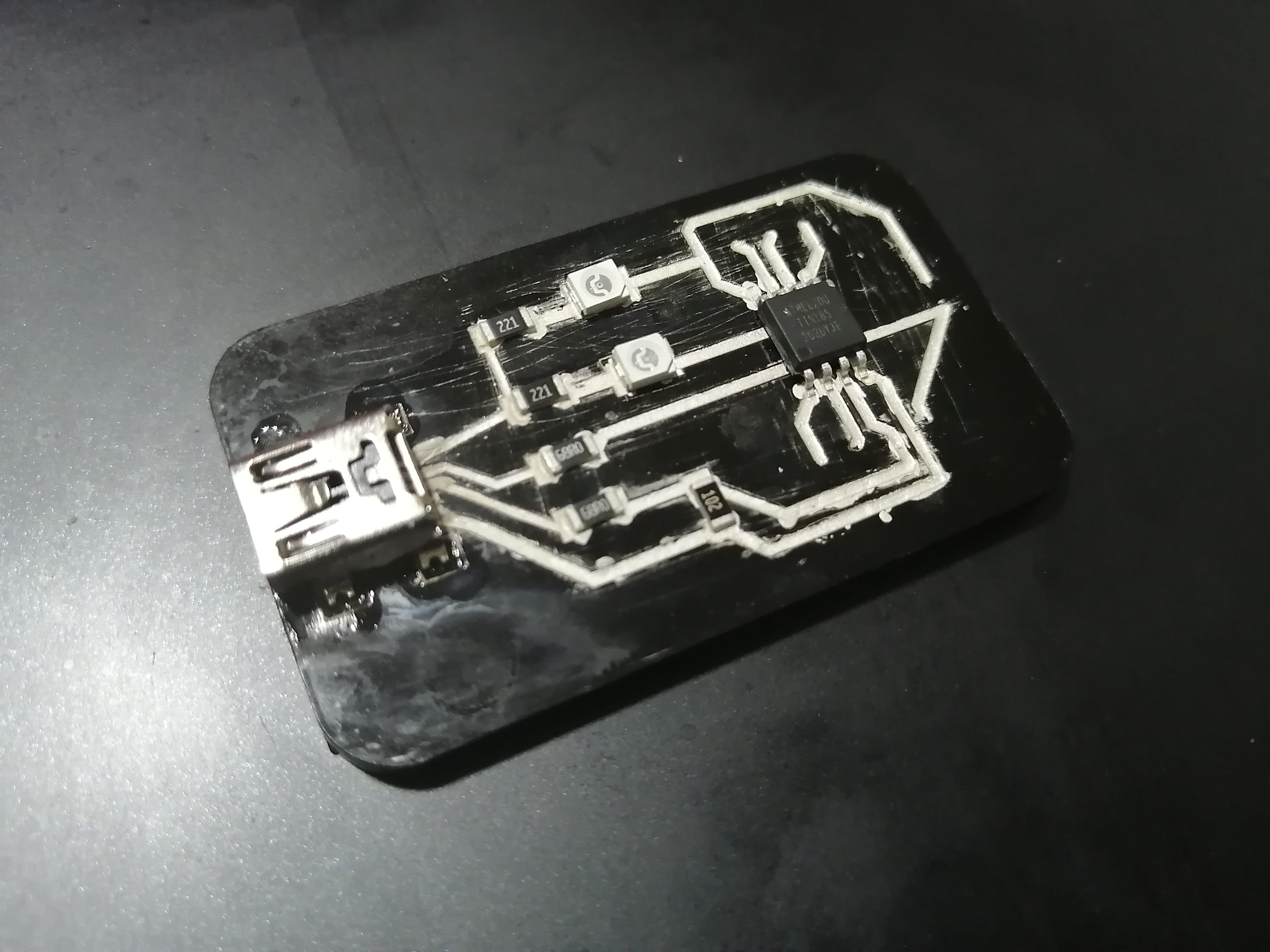
So, this No-soldering method of making PCBs works! Here’s the final shot of the PCB:
Lesson learned and what can be improved
The paste takes a long time to dry and this gets worse as the conductive layer thickens, like a couple of days. Blowing hot air does not seem to improve the drying time. This makes it not suitable for rapid prototyping.
The consistency of the paste and its stickiness make it hard to work with this method, more liquid, and fast-drying paste or conductive ink would be better. I’ve tried making my conductive ink, but getting the materials in Peru for testing is very difficult!
I thought that the excess conductive paste could be easily wiped off like in the intaglio process, but this proved to be not the case. The stickiness of the paste makes this even more difficult. Although the solder mask improved this step another conductive paste alternative should be explored to fit rapid prototyping.
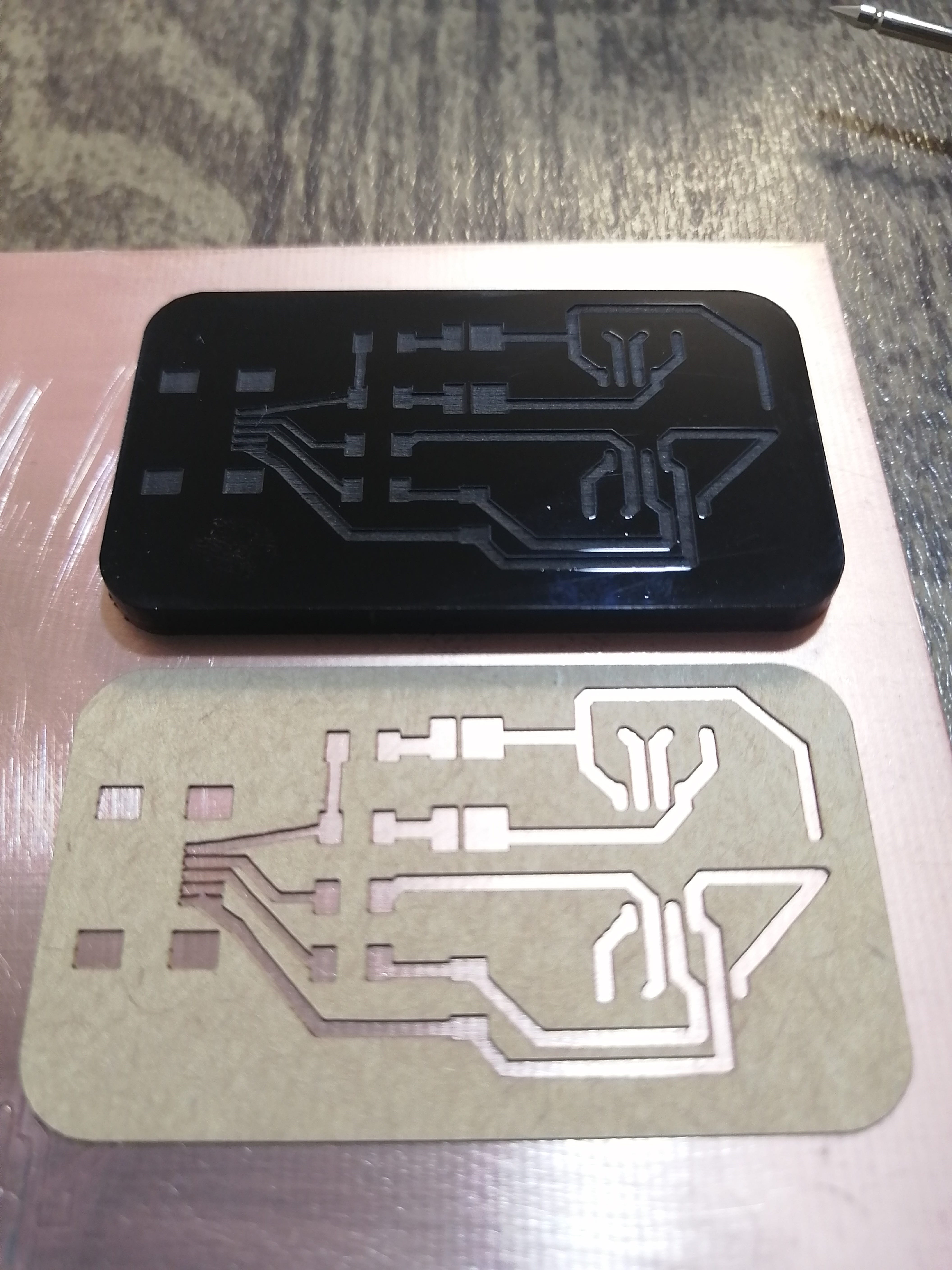
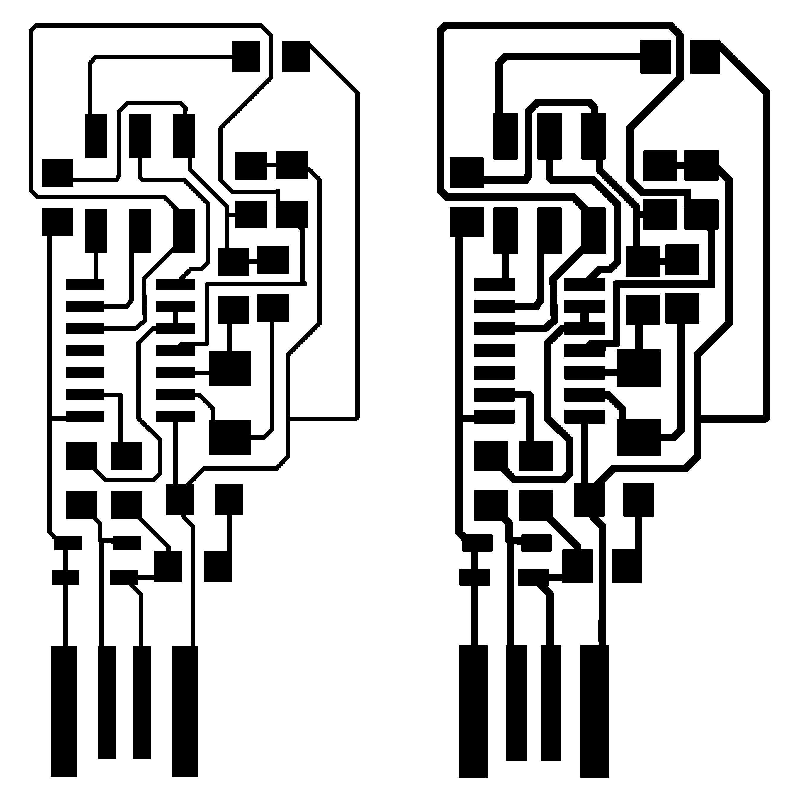
More testing is needed to improve conductivity, the traces design should be wider and shallow, this is easily achieved working with the same .png file on an image editing software. The power of the laser engraving could also be tuned to make a shallow engraving. This was made in the second PCB having wider traces and a shallow engraving profile (around 0.2mm) this improved the time invested in component placing.
Here is an example of the original .png ISP file (left) and the traces made wider with a 5x offset.
To improve the coverage of the traces, not waste conductive material, and avoid making a mess maybe a disposable stencil should be used like in silkscreen printing or when placing solder paste on PCBs
I’ve also tried a cutout of the ISP in thinner acrylic to be able to connect it like a USB but the engraving and cutting power curved a little the acrylic. So, have in mind!
An encapsulation with epoxy resin could be used to secured the components to make a fully functional PCB board.
There is a possibility to make multiple-layer PCBs with this method, holes could be easily made in acrylic with the laser cutter.
Files
Download the PCB file for engraving (.svg) here