Group assignment
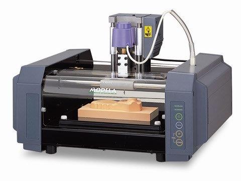
We started testing the milling machine available in the FabLAb ESAN, it is a Roland Modela MDX-20, this is a 3D milling machine with also a scanning function.
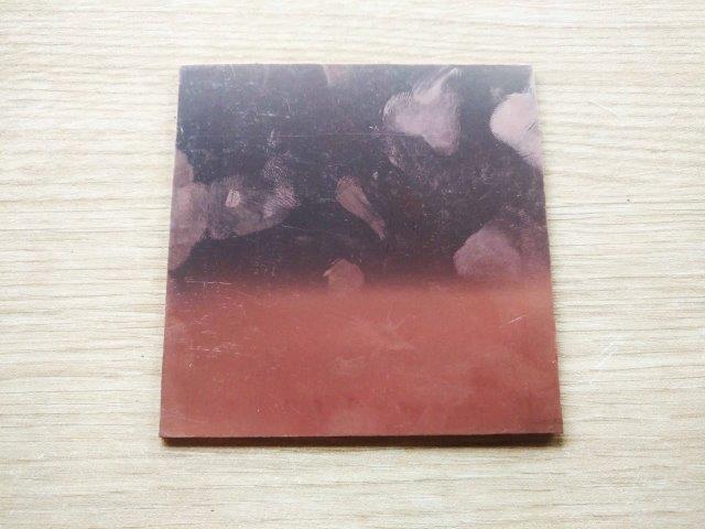
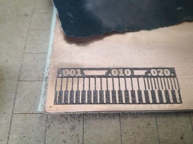
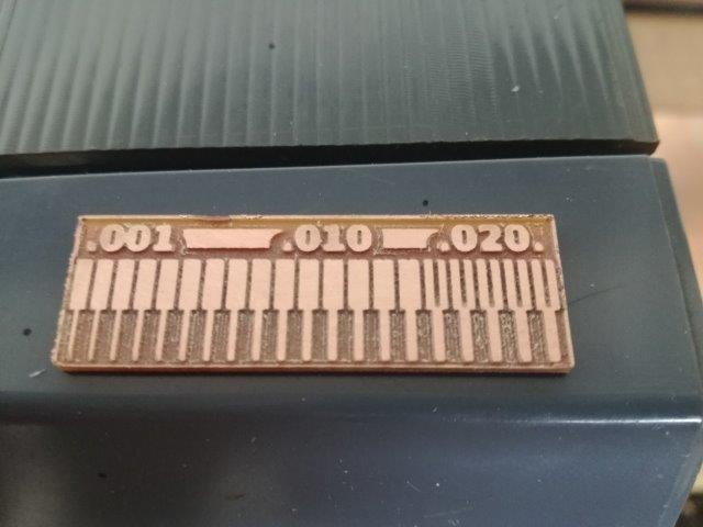
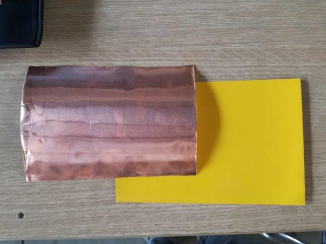
As milling material, we used a single-sided copper square plate of 100mm, and for the test templates, we used the files available here: one for the traces, and one for the outline of the board, both in .png format.
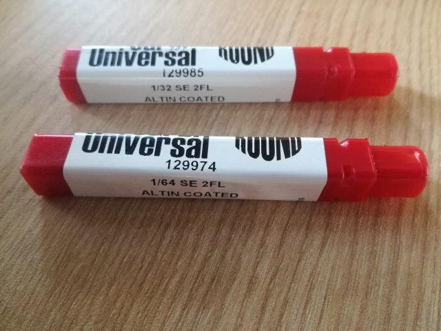
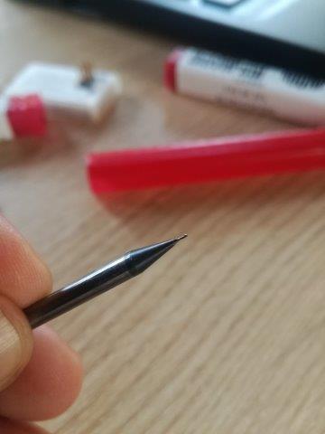
The milling bits available in the FabLab were one 1/64" (approx. 0.39mm) for the traces and a 1/32" ( approx. 0.79mm) for the outline.
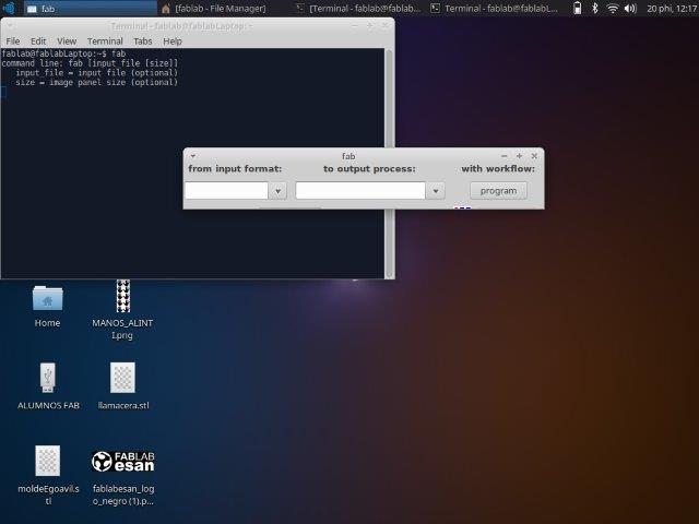
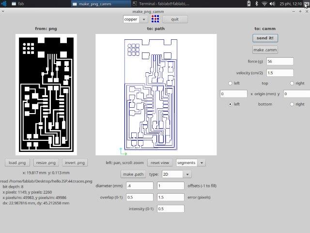
We need to convert the .png templates to a milling pattern so, we used the locally installed mods (for Linux) in the PC next to the milling machine.
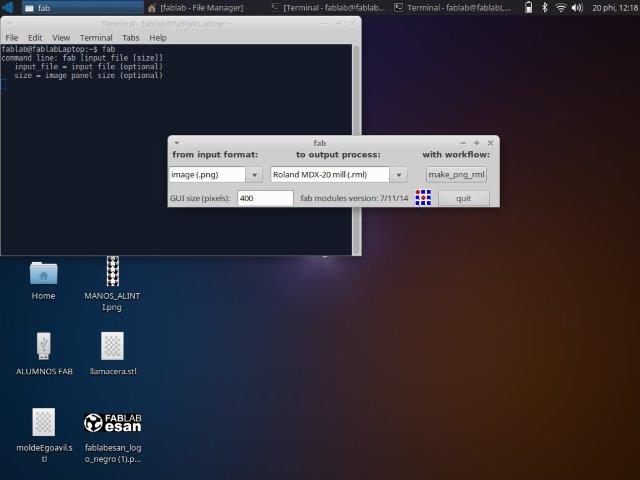
The steps are almost the same as the ones used for the vinyl cutting assignment, we first open the terminal and type sudo fab command to open the application. This opens a small window to select the input format (.png image), the output process (Roland MDX-20 mill (.rml)), and the workflow make_png_rml.
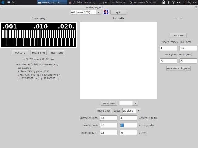
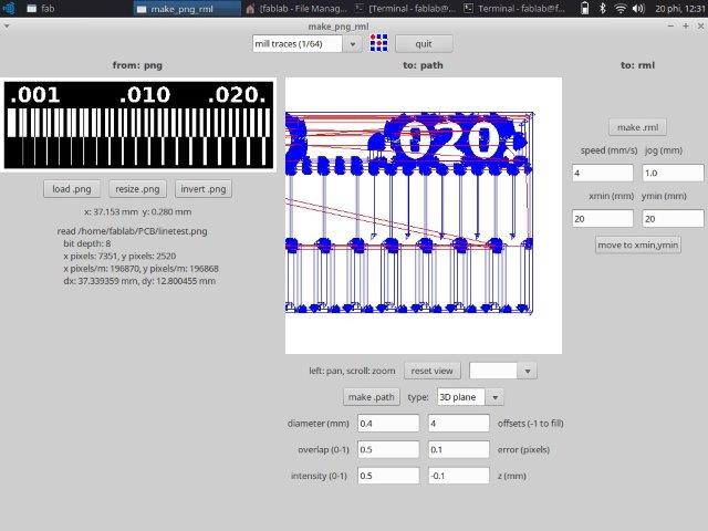
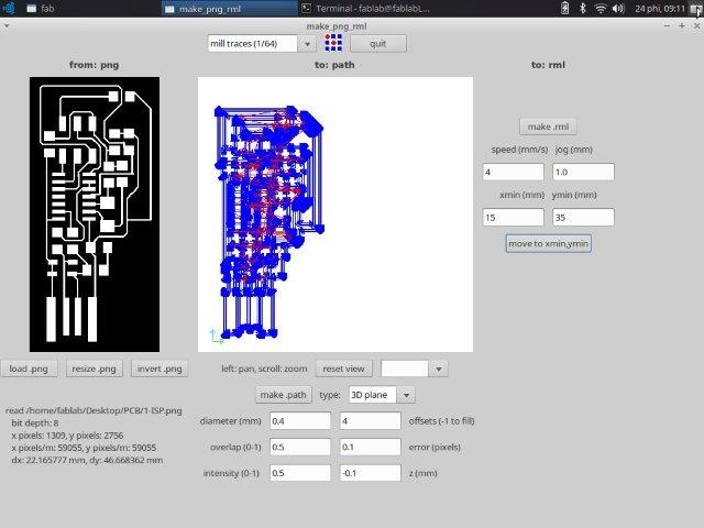
This opens the interface, next, we load the .png image (first we select the milling traces file) and select the mill traces (1/64) option from the top panel to indicate the process and the milling bit we'll be using. We then change the error(pixels) value to 0.1 (it was set at 1.1 by default).
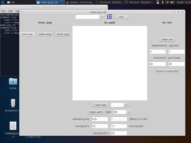
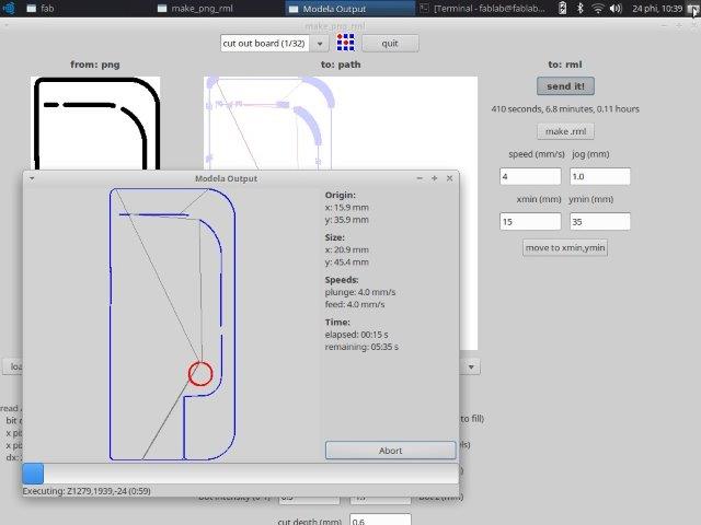
Another very important factor is the X and Y coordinates, this would be set according to the position on the copper plate on the machine, this will set the starting point of the milling bit. We set this point to 20 / 20 and use the move to xmin,ymin button to automatically place the bit into position. These X and Y numbers need to be the same when using the outline file to cut the board!
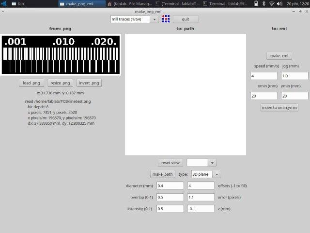
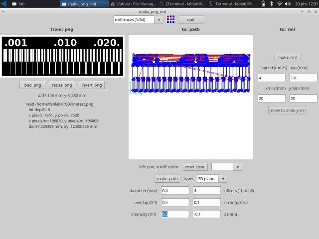
We used the default settings for speed (4 mm/s), jog (1 mm), diameter, overlap, offsets, intensity, and Z as this is our first test run on the machine. Then, we hit the make.path button, this will generate the milling path of the tool.
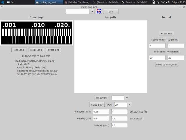
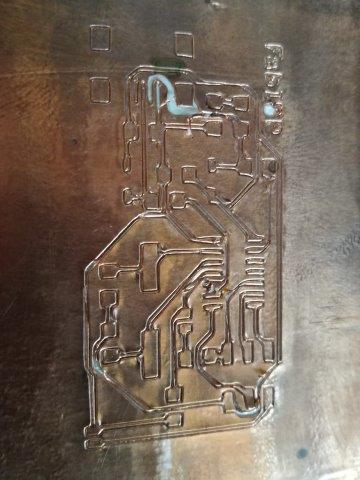
Once we hit make.path, the path is generated in the window next to the .png image, this works by recognizing the white parts of the image and then milling the outline 4 times, (this value is set by default to 4 offsets) but we can change it depending on the characteristics of the PCB design. The blue lines indicate the milling path, while the red lines indicate the traveling of the tool.
A closer inspection on the paths...
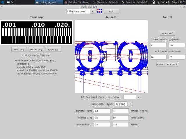
A closer inpection on the paths between the pads, the lines indicate that the milling bit will go inside.
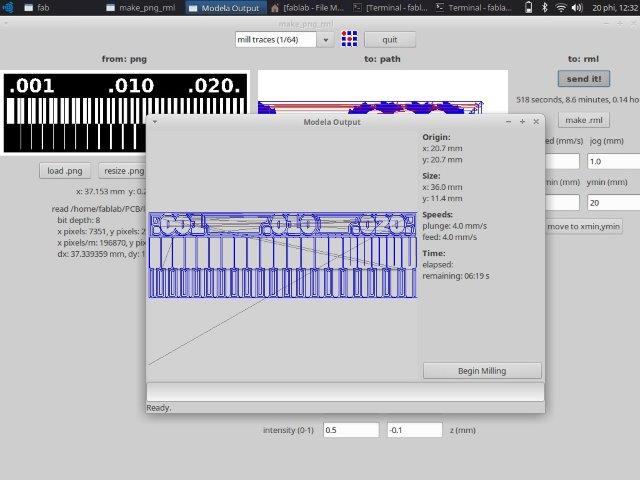
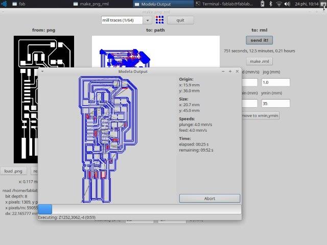
After pressing the make .rnl the send it! button appears.

In the paths window, we can zoom in and inspect the design to prevent flaws that might occur while milling. For example, we noticed that for the traces the milling bit can only go inside the last five parts under the .020 tag.
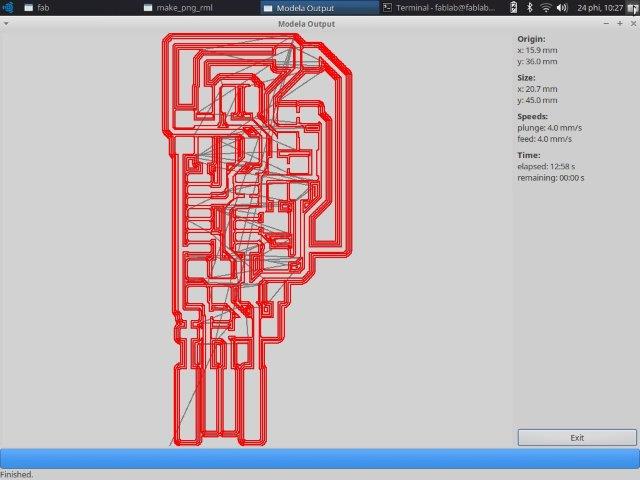
After inspecting the paths we hit the make .rml button to generate the milling file and then click the send it! button to begin the milling work. This last action opens a new window called modela output where we can see the movement of the milling tool, this also gives an estimated time of milling.
We repeat the process for the outline file that will cut out or test from the copper plate, but this time we select the cut out board (1/32) option on the top menu. Notice that this will vary the default settings, like offset is now set to 1, and there are new fields like top Z, bot Z, and cut depth in mm. also, the intensity is separated in top and bot fields. The speed and jog parameters remain the same as with the traces.
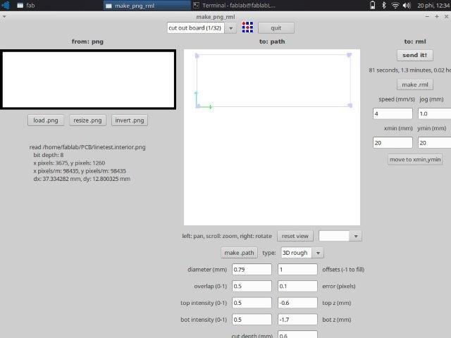
After we change the parameter of error (pixels) to 0.1 and double-check that the X and Y coordinates are the same we used in the previous file, we can press the make.rnl button and then send it! to the milling machine.
Here goes the machine setting up part
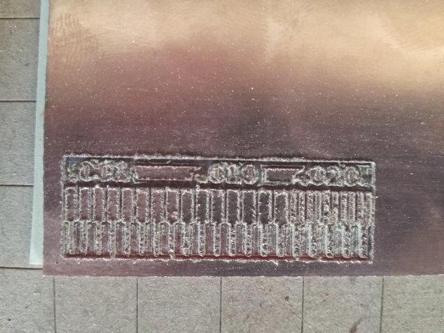
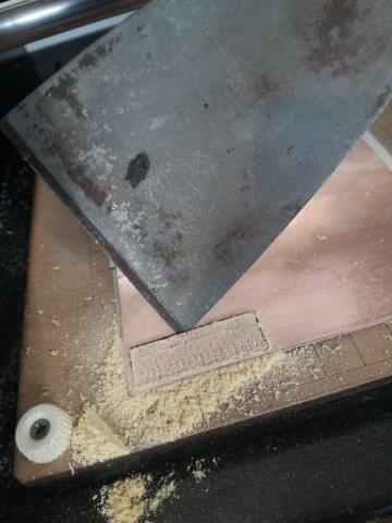
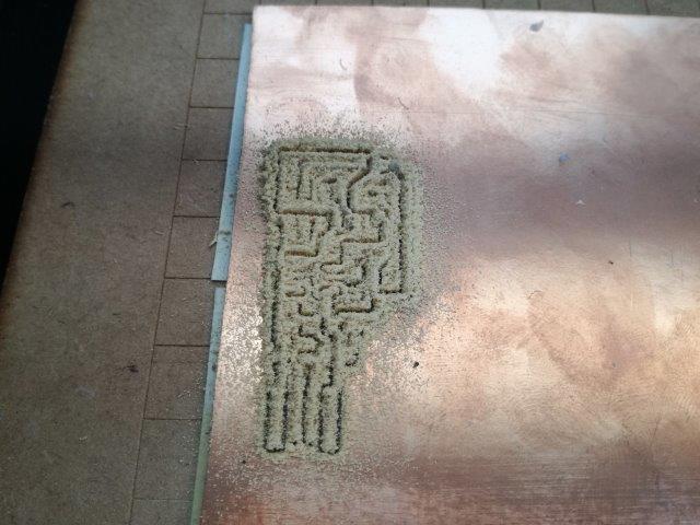
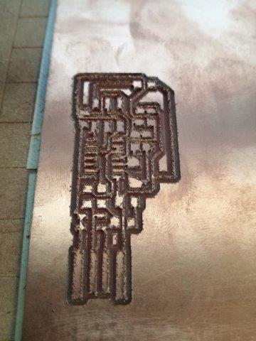
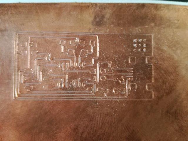
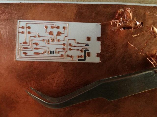
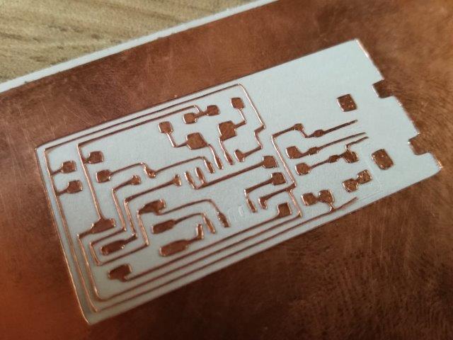
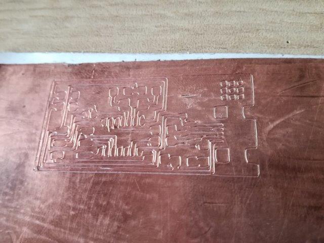
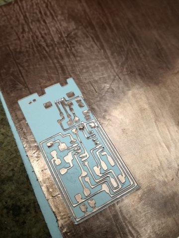
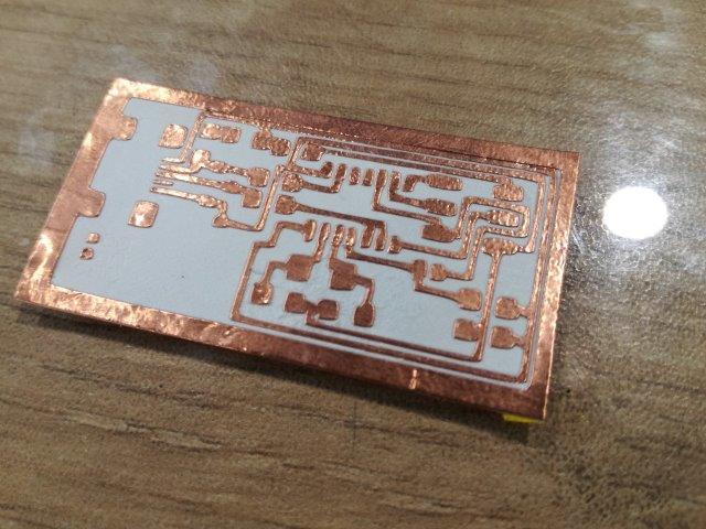
After the traces milling process ended we press the view button on the machine to inspect the finished piece, we carefully brush off the milling residue and noticed that the edges on the trace have a rough finish.
This is caused by using a cut-up milling bit that forces the copper traces to bent upwards. This was fixed by sanding (with fine grade sanding paper) only a couple passes are enough, this process is called deburring.
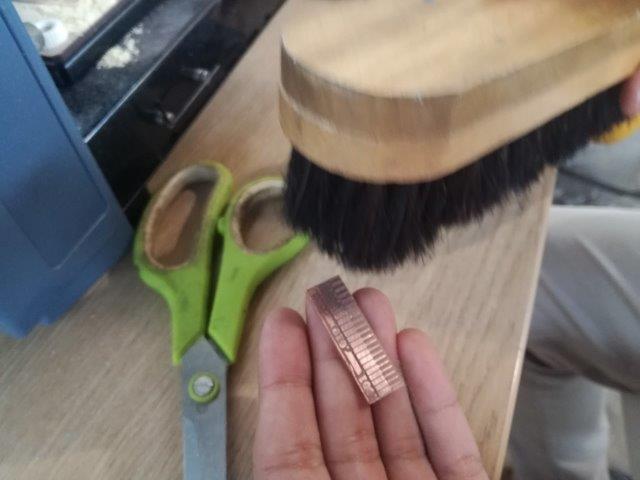
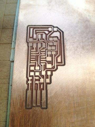
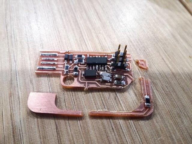
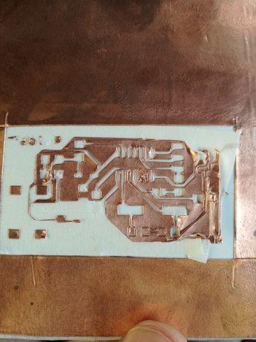
After the cut-out process ended we press the view option again to inspect the finished piece, brush off the milling residue and separate the board from the plate with a paint scraper.
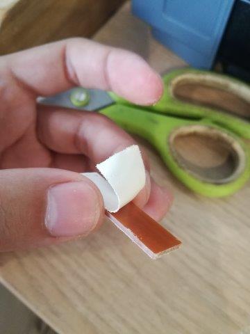
After peeling the double-sided tape, and cleaning we have our finished test board!
Making a FabISP
For this week's assignment, we'll be fabricating a FabISP, but if you are new to ISP's (like me) I'm sure you'll be wondering what exactly is an ISP. Be sure to check out this guide by Ali Shtarvanov to understand the components of an ISP. And this page from SheekGeek with a pretty neat example and also this page about building one.
So, the FabISP is a programmer based on an ATTiny microcontroller, that allows programming other microcontrollers.
The assignment is to build a FabISP including:
- The fabrication of the PCB
- Soldering the components
- Programming the ISP and prove it works
Let's begin!
Choosing the FabISP design
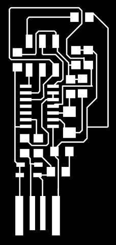
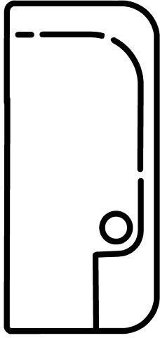
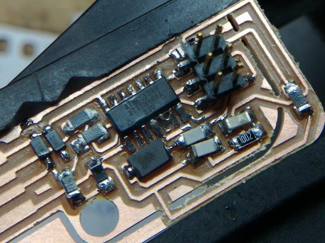
The assignment does not include designing the FabISP so, I'll be using one from the FabAcademy Archive based on the ATtiny44.
I choose the Valentin Heun design because it looks tiny, and its the only one that has a detachable part, and I want to try this feature.
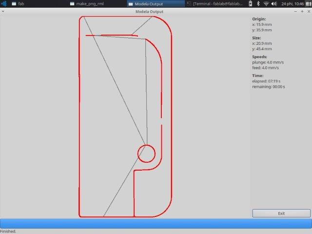
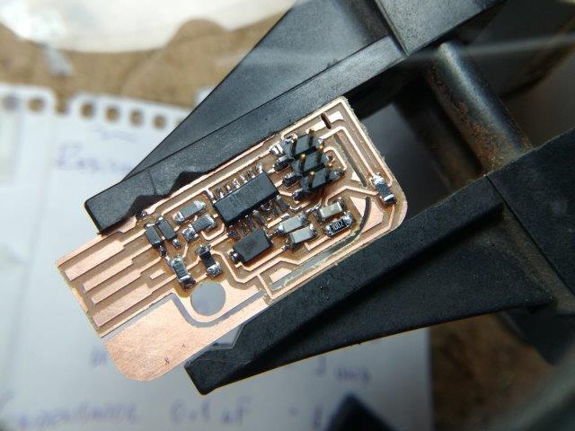
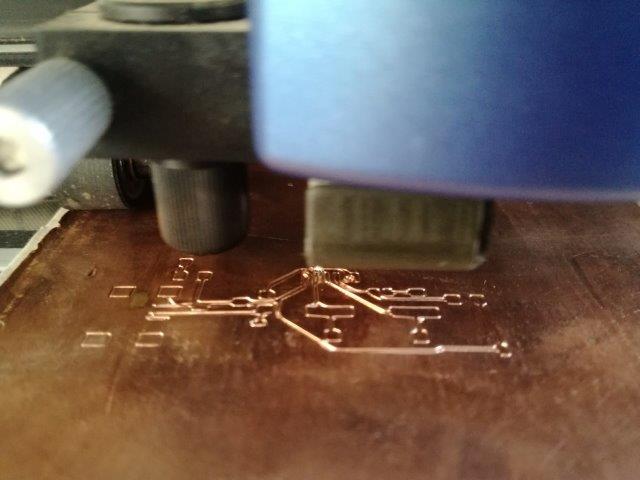
Milling the board
For the milling, I used the same procedure as the test board in the group assignment. I used the same copper plate that we used for the traces test to cut my ISP so I set the coordinates to star the milling at 15 /35. All values like speed, jog, and intensity are set by default, only error (pixels) is set to 0.1.
After making the path I began the X and Y positioning, then for the Z-axis (set the bit to the plate), I used the up and down buttons until the bit did a small mark on the plate. Once the 3 coordinates are set I generated the .rml file and hit Send it!
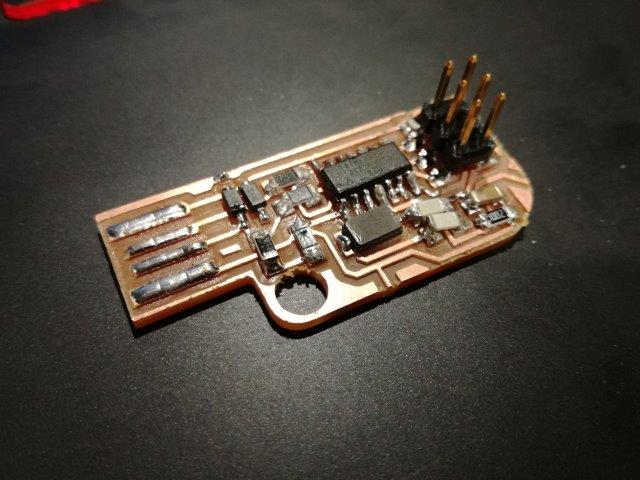
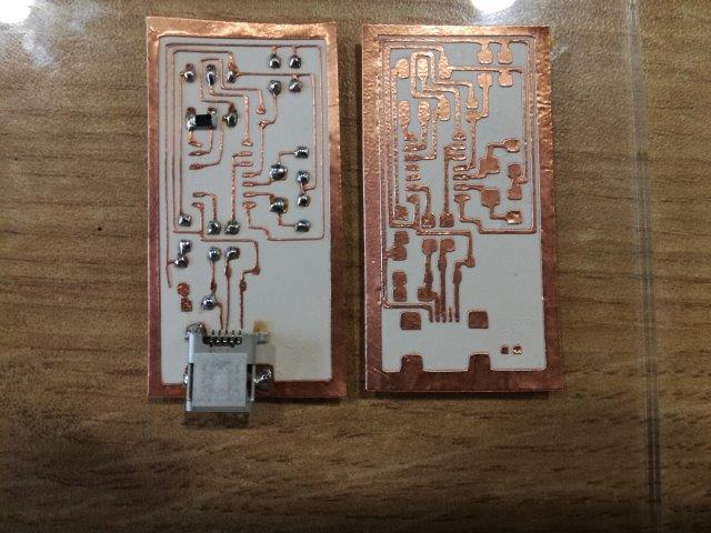
The complete traces milling took around 13 min. then we press the View button to inspect the finished job.
After a quick clean up (with a small vacuum) the FabISP it's a little bit rough on the edges, so gentle sanding (by hand) is applied. Here is the before and after deburring:
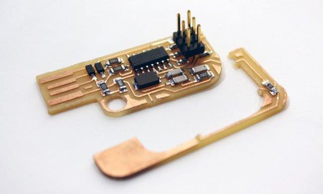
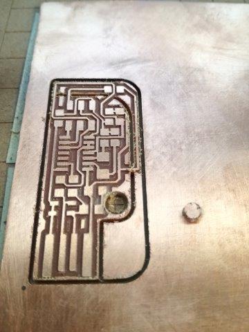
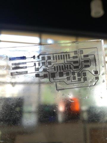
The outline milling is made following the steps, but changing the process (and the bit) to cut out board (1/32), the special thing about this design is that it has a hole for the keychain, and son carved lines to break the board after the programming, cutting put the fuse. The job took around 7 min.
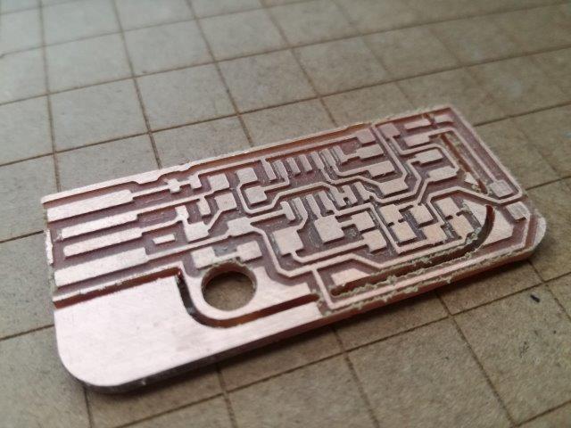
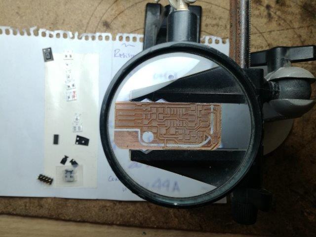
After the cutout, the inspection, some deburring, carefully taking out the board from the plate with a paint scraper (trying not to break the carved parts) and peeling the double-sided tape… Here it is the finished board, ready for soldering! or is it?
Do all the traces look good? Is it milled like the design? The answer is yes to both, but I spotted a minor flaw in the milling process that caused a join on two traces.
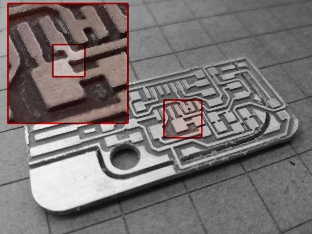
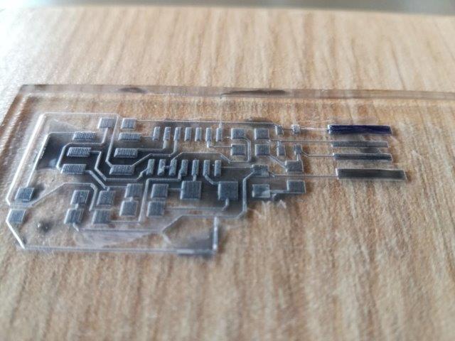
This was fixed using a cutting knife to do a little incision on the union. I made this with the help of a magnifying glass being cautious not damage the traces.
Some notes: The movement of the milling bit seemed erratic, doing some milling dots and jumping to other spots without completing the trace offset. There's some way to fix this?
Soldering the components.
Unfortunately, Valentin's design does not include a file for the FabISP in Eagle or any other software, but it does have an assembly guide pictured here where we can get a list of the components.
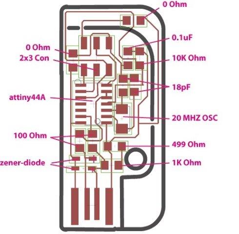
List of components:
- 2 x Zener diode
- 2 x 100 Ohm R.
- ATTiny44A
- 2x3 Connector
- 2 x 0 Ohm
- 0.1 uF
- 10k Ohm
- 18 pF (not on inventory, so I'll be trying 10pF)
- 20 Mhz OSC
- 499 Ohm
- 1K Ohm
Upon checking the list with the FabLab inventory, the instructor suggested that I could change the 18 pF condensers to 10 pF and still fabricate the board. This is the list with the components attached to double-sided tape.
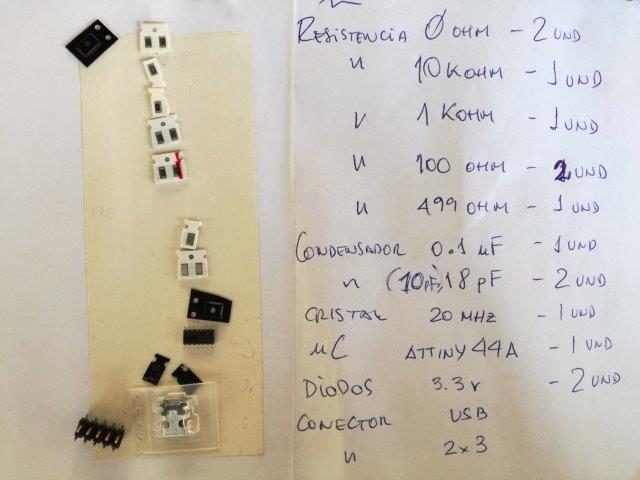
I've never soldered SMD components before so I was kind of worried about how tiny these are. I prepared my soldering materials on the table, this included: a helping hand, lamp, magnifying glass, pliers, cutter, soldering iron and flux.
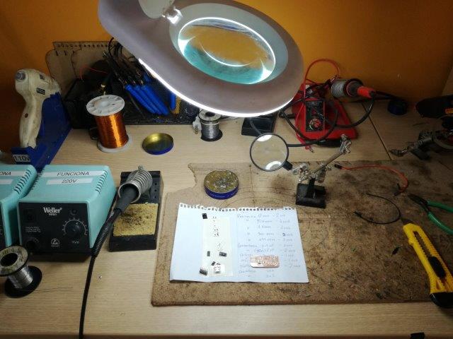
The soldering station is a beautiful Weller WES51, but I was a little worried about the soldering tip…
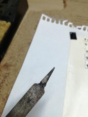
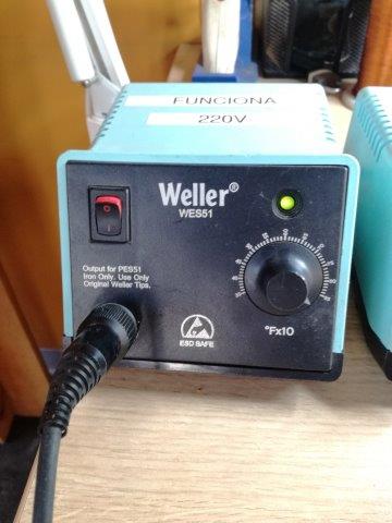
After a brief discussion with the instructor, he assured me that the soldering tip was OK, and after a little cleaning, I would be able to solder with it. So a couple of flux - sponge cleaning - soldering cycles, and with the board secured I was ready to solder.
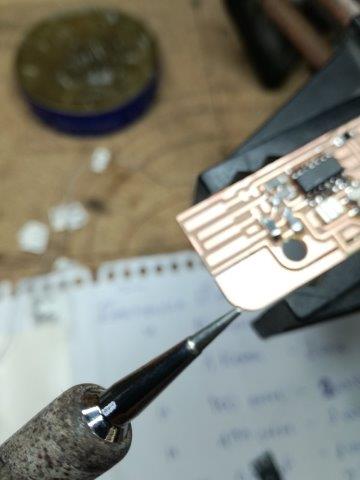
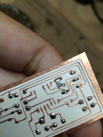
I started with the ATTiny since this is in a central position on the FabISP, and it's supposed the hardest component to solder.
So far so good? well, NO. After the ATTiny, I began soldering the components in my list order. This became increasingly difficult as the resistors are very hard to hold, and my damaged soldering tip was only heating from the side, and NOT on the tip. This was causing some cold soldering as seen in the resistors under the ATTiny.
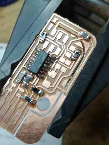
After soldering most of the components, and show the instructor that my components were looking awful, they gave me a new one. Ah! look at that fresh tip!
Thankfully the Zener diodes (the smallest component) were soldered with the new tip, and also the oscillator and the 2x3 connector.
For the finishing touches, I added solder to the USB connectors and cleaned up the copper residue on the USB tip with a cutter.
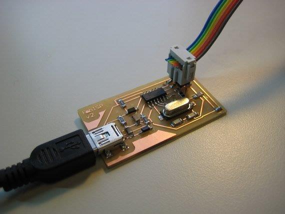
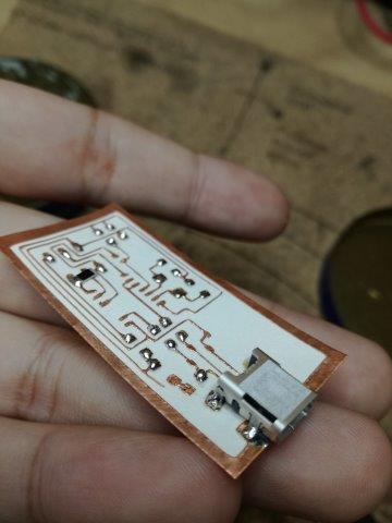
The finished FabISP:
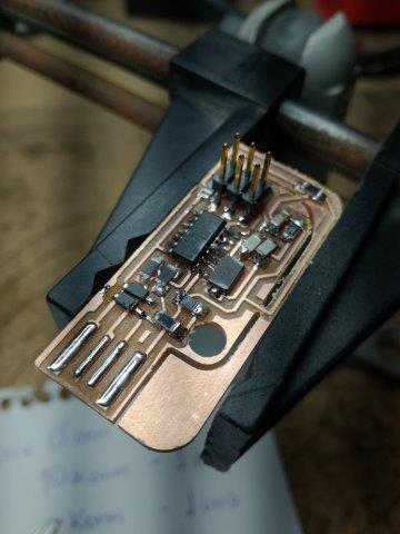
Some notes: The files from Valentin does not show the orientation of the ATTiny or the diodes, so I've used the photos of his board as a guide. As a contribution, I'll be doing a custom design file for the board and uploading it here soon.
Now, next to the programming part… Will it work?
Programming
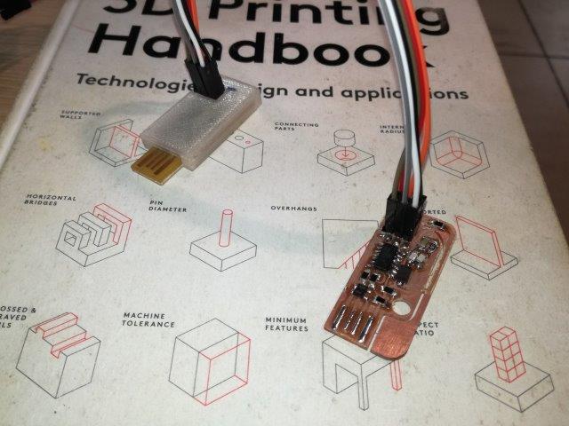
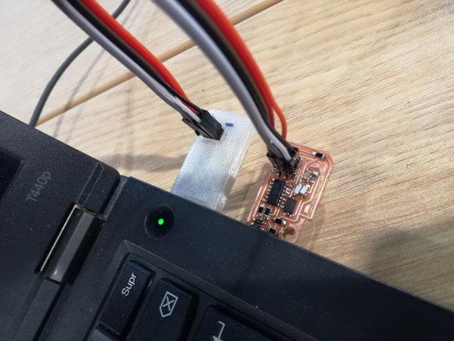
For the programing, I used the instructor's FabISP, this was connected to the new FabISP using jumpers being careful to follow the exact order on both the connectors.
I used the PC of the FabLab that runs Ubuntu, and this tutorial as a guide and also this tutorial.
Download and install the software for AVR programming
The PC already had the AVR programming software (AVRdude) installed and GCC software and dependencies.
I proceed to download and Unzip the Firmware form here
After unzipping the firmware, I proceed to Edit the Makefile from the text editor, this is made changing the "#" symbol to transform the code line to commentary or vice versa.
#AVRDUDE = avrdude -c usbtiny -p $(DEVICE) # edit this line for your programmerAVRDUDE = avrdude -c avrisp2 -P usb -p $(DEVICE) # edit this line for your programmerNext, we compile the firmware. and Type: make clean
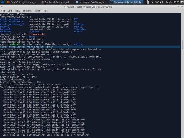
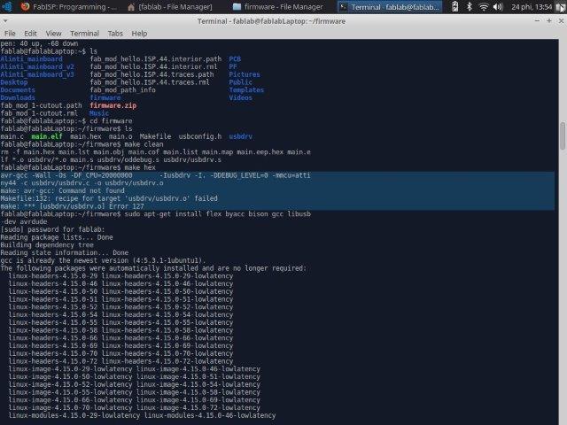
Type: make hex (note that this doesn't work, because I needed to install the dependencies first. See some notes at the bottom of this tutorial)

In the picture below, we see the error line and then the command for installing dependencies:

After the successful installing, type: make fuse. whoops! another error, this was because the new FadISP was not correctly connected to the USB port.
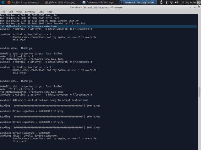
After making sure the FabISP was making enough contact with the USB port the make fuse went right.
This is the line that confirms the command.
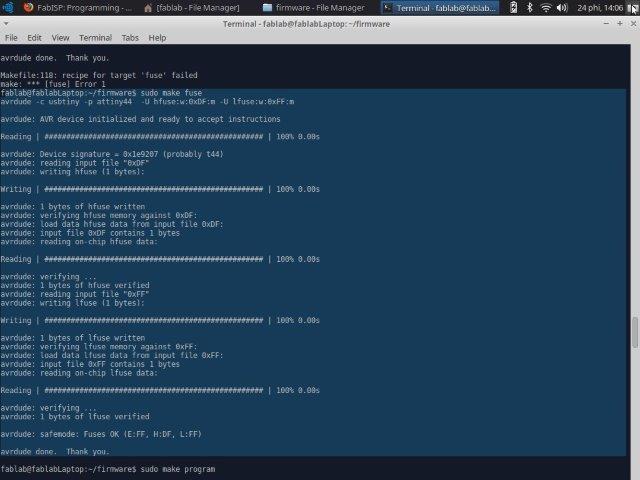
Next, we are ready to type: make program.
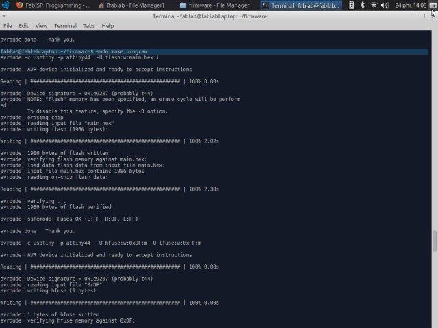
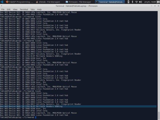
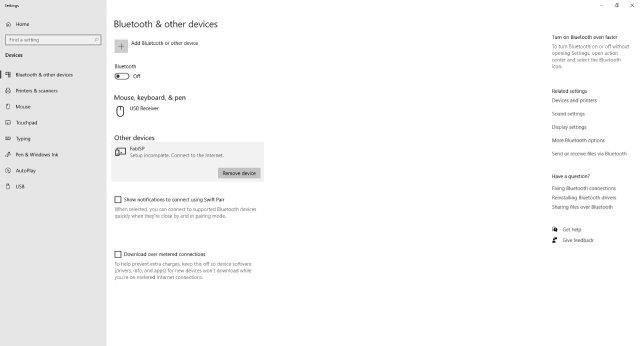
Success! the images above show the correct programming of the FabISP and the USB port detecting the device (command lsusb). The device is also detected by my Windows PC.
It is now time to break the fuse.
My New FabISP is ready to program!
Some notes: The first issue was that the new FabISP was not connected to the USB port, instead I connected the instructors FabISP. I cut the part of the USB connector to fit the USB port to be able to connect the new FabISP.
I got confident and tried to run the commands without installing the dependencies first! This resulted in failed commands.
The make fuse command wasn't working. turns out the new fabISP was loose in the USB port. I pushed it upwards with my hand and it worked. The same was applied when trying to connect the newly programmed FabISP and the USB didn't recognize it. But this issue is more or less on the USB side.
Copper tape for flexible PCB?
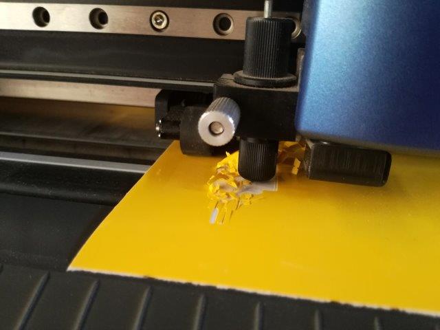
I tried the vinyl cutter to make the same FabISP design I'll be milling. Since I want to test the resolution of the cut first, I've used yellow vinyl.
A couple of attempts went bad, the cut was made, but as the knife moved through the design all the traces were lifted and tangled. I've tried fixing this issue first turning the cutting force from 45 to 30, and later decreasing the speed from 5mm/s to 1mm/s.
The slower speed seemed to work better for finer details, but at some point, the cut tangled and ripped.
I figured this was not a cutting issue in itself as I could see that the machine was cutting the traces, but more of a material issue, since vinyl is meant to easily lift from its paperback. I asked for a cutting mat or any sort of substrate that could sticky the vinyl more firmly for the cutting, but the FabLab did not have any, so I've decided I would run some test in a made-up material to test the idea.
I've bonded the sticky part of the vinyl to the sticky part of a paper transfer sheet, as I noticed this came up too thin for the vinyl cutter, I added layer from the discarded vinyl paperback and glued it together for a triple-layer material. Next to the vinyl cutter, I used the same setting (30 force, 1 speed) to send the job.
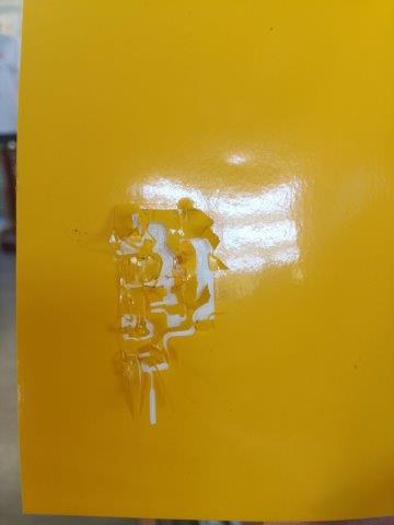
The result was very promising as the vinyl did not lift while cutting. Now, as this was only a cutting test, I did a weeding process but to lift the traces. The final result was good, but some spots seemed to have some trouble.
After lifting the traces I noticed that some were too close together, this might indicate that the vinyl slightly moved, or that the traces are too thin for the vinyl cutter (or the material). Strait traces (horizontal and vertical) were clean-cut, but diagonal traces seemed to have issues.
After some more tests on vinyl, I was ready for the copper tape, so I've done a test on the material as it was, without additional sheets or transfer. It did not work, as soon as the tip started cutting the traces lifted.
The second attempt was made sticking the copper to transfer paper, (both of the sticky sides together), and lowering the speed of the cut to 1.5. This test was ok, you can even see the letters!. Notice that this time I was using the FabISP design as its bigger and has more space for the traces.
I've tried the same process of weeding the traces to test the cutting cleanness (and also cuz I did not cut the outline, so weeding would be impossible). I got some minor flaws in the cuts,(need a bit more force on the cut)but it looks that I was making some progress.
Also, the substrate was too glued together, so the weeding process would do minor rips to the paper and made it difficult to separate traces from residue.
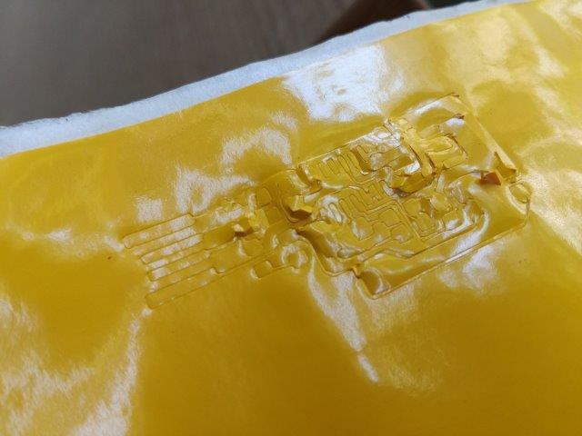
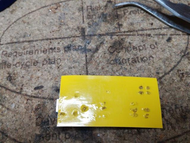
For the third attempt I wanted to go all-in, so I made a new substrate sticking the copper tape, to the back of the yellow vinyl.
This time I changed the image file to invert.png, the force set to 56 (default was 55) and the speed to 1.5(default was 2.5)

The cut was good but the weeding took some parts of the traces… Anyway, maybe the traces were too thin for the substrate I was using since the pulling of the residue has a lot more area, some of the traces are easily lifted or moved with it.
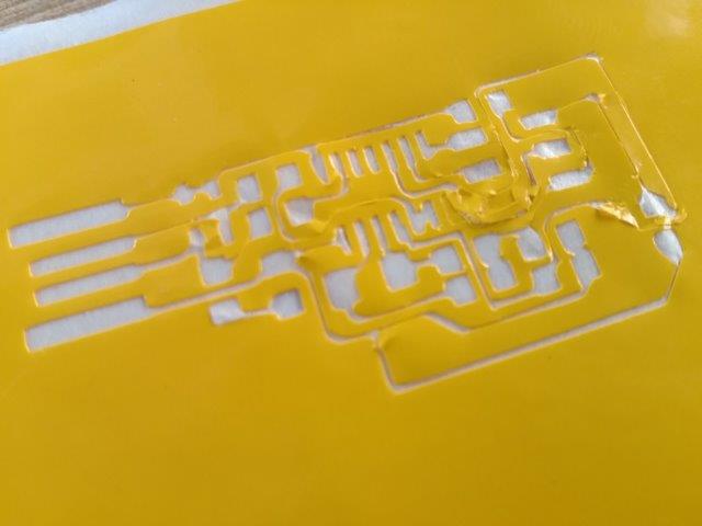
The next step was to make the traces wider, as I did not have time to make it on raster software I used the diameter(mm) parameter in Mods to change how the software would interpret the pixels. I tried several settings and inspected the different paths until I was happy with a 0.4 setting (default id 0.25).
Now, look at those chunky traces! easier to weeding for sure, and it even cut the CBA logo.
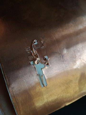
I ran some solder test on the previous circuit, as I was worried about the fine traces and the glue from the copper tape to burn while soldering components.
It went better than expected. Only the backside of the board (vinyl) suffered a little from the soldering heat, but we can peel this off later.
Unfortunately, I did not have time (or components) to solder test the chunkier traces. but will doo soon!
Some future milling test:
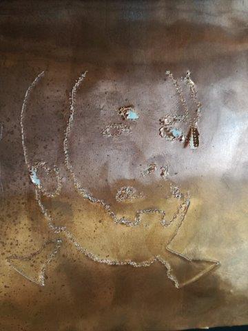
I wonder about the capabilities of the machine for art projects, because the copper plate for the PCB is similar to the material used for printmaking, so the milling machine could be used to replicate a drypoint technique.
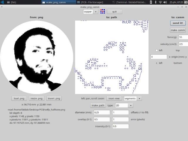
While the offset parameter is useful for PCB milling, to create a replica of a drawing we'll need to use the fill option, to completely remove the material, typing -1 on the offsets box. I used a self-portrait halftone image to test this feature.
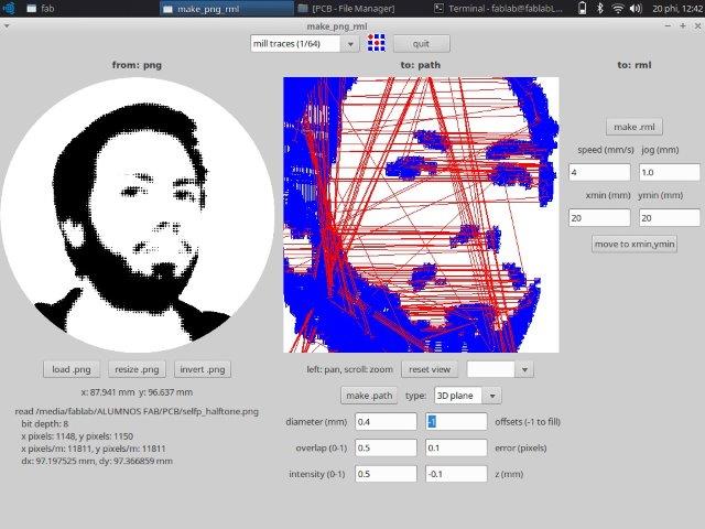
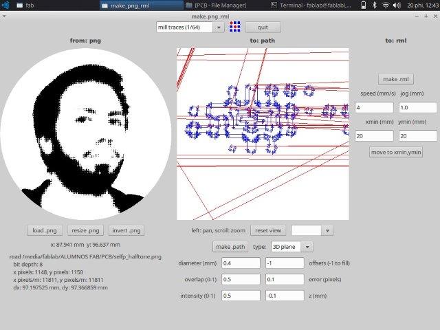
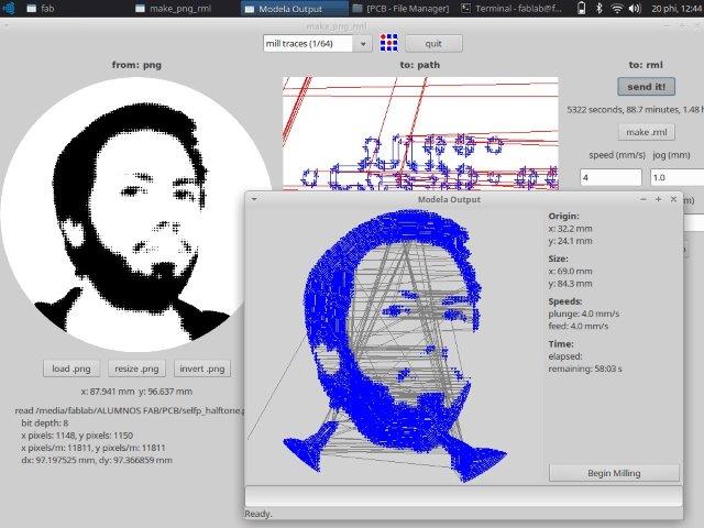
I wanted to mill the design but did not want to waste a complete copper board, so I'll try to use laser-cut acrylic with copper vinyl attached.
I'll try to configure the output settings to make traces milling with the 1/32" bit, to make it go faster? but maybe it's not the best idea for resolution.
Bonus 01: Acrylic PCB test
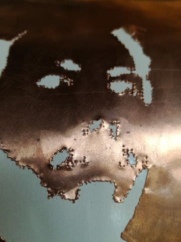
As I was getting a little frustrated with the copper tape, I tried engraving acrylic with the FabISP design, since the engraving creates small canals in the material, this could be used to fill with a conductive material, like solder paste (and later being transformed with the hot air gun) or conductive paint, like doing printmaking.
Unfortunately, the FabLab did not have those available so I did a proof of concept with black photocuring resin, this ended up making a bit of a mess but it did go into the engraved traces.
Bonus 02: Halftone with the Roland
Since I could not engrave my self-portrait with the milling machine, I decided to try the vinyl cutter instead, to see how it reacted to the "dots" on the halftone image.
It went well, the cutter does some kind of dot marking and cutting following the curly pattern, so there's a possibility here to try some cleaner halftone pics.
Bonus 03: New mouse pad?
Without noticing it, I placed the tiny test board under my mouse, and worked like a charm, the movement felt incredibly light, as it was flying through the mouse pad with almost no resistance. I'll be using the milling machine to cut some new contact points for my mouse from the copper plate material.
Useful links:
- Falstad Circuit simulator
- Why 0 Ohm resistor? (Spanish)