week 3: computer-controlled cutting
week 4: electronics production
week 5: 3D scanning & printing
week 8: computer-controlled machining
week 13: networking & communications
week 14: interface & application programming
week 15: applications & implications
week 16: mechanical design & machine design
This week we're taking what we did in week 4 and going back a step further. The assignment is to design the schematic for the "hello world" board, route the traces, then mill and stuff the board as we did previously. With practice, this whole process should get to the point where it takes only about an hour ... or so I've heard.
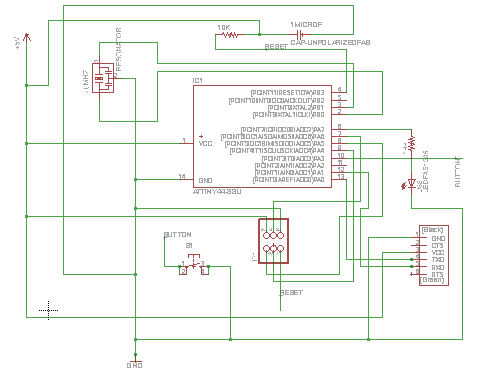
Using EAGLE to design the schematic involved finding the components in the fab library and making all the connections using the net function. This was occasionally frustrating, as connections that I thought were made weren't actually made, and I had to keep grabbing components and moving them around to be sure. In the end my schematic looked like this:
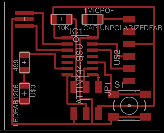
The next step was to take the schematic and turn it into a board design, routing all the traces. Shawn described this as like playing a game of flow, which was pretty accurate, except EAGLE had added eccentricities like making sure to use the right grid size. In the end my board looked like this:
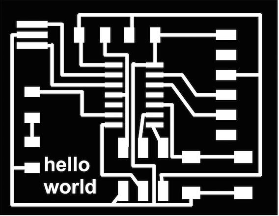
Finally I used The GIMP to make the png file for the traces:
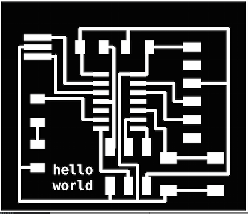
So this was the first board that I milled, but it came out with some problems. First, the letters in the "hello world" were too small and so tore off the board. More importantly, some of the traces were awfully thin, so I was worried the connections wouldn't be made. And most importantly, the border traces didn't create any paths at all, so I couldn't cut out the board.
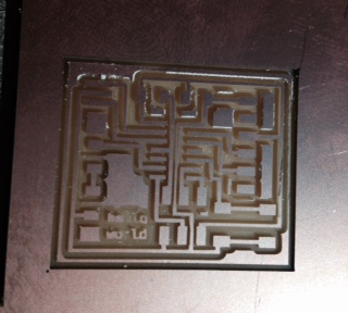
Since I had to edit the file for the border anyway, I decided to go back to EAGLE and fix the traces too, moving the components apart and making the whole board a little bit bigger.
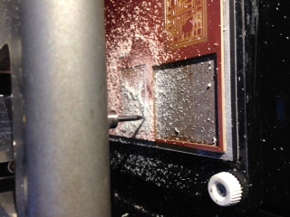
This one went through the milling process much better.
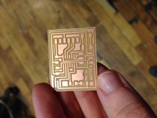
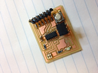
The one part of the process that I have gotten much quicker at is soldering. The finished board looks pretty neat.
Jenny Kostka Fab Academy 2015
