
week 3: computer-controlled cutting
week 4: electronics production
week 5: 3D scanning & printing
week 8: computer-controlled machining
week 13: networking & communications
week 14: interface & application programming
week 15: applications & implications
week 16: mechanical design & machine design
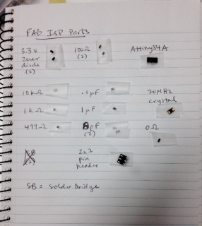
This week was the first in which we were not really designing anything, but producing a programmer (ISP) circuit board from a pre-made design. The skills involved were milling the board, stuffing the board, and programming the board. Altogether, I made three ISP circuits, using two different designs and two different techniques.
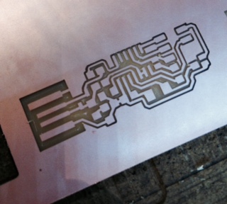
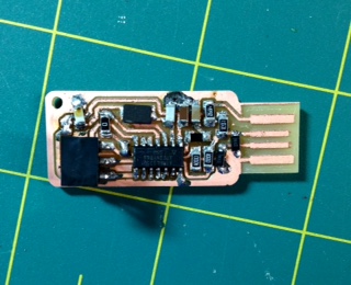
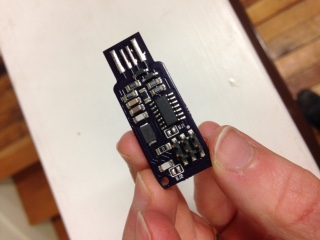
The first one I made used the ISP key design, where the USB connection is part of the board, not a separate piece.
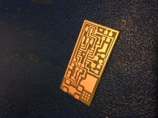
The first step was to mill the board, which took a couple of tries for me to get right. The hardest part was zeroing the z axis on the milling machine by lowering the bit until it just touched the top of the FR1 board. It was really hard to tell when the bit was at the proper height, and as the copper layer on the FR1 is only 0.1mm thick, there wasn't a lot of room for error. After a couple of tries, though, I managed to mill the board's traces.
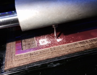
After the traces were milled, the next step was to change to bigger bit and cut out the outline. This is where I had my biggest failure - I didn't tighten the bit enough when I changed it, so it went through the FR1 and into the sacrificial layer beneath, slowing down enough that it got very rough and ended up cutting right across the traces.
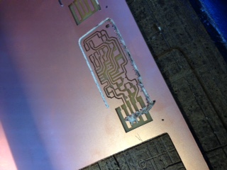
On the second try, I successfully milled and cut out the board, then stuffed the board, soldering all the components on. I had done a little bit of soldering before, but never surface-mount components, and never components that were so small, so my technique was pretty messy at first.
This meant that programming the board required some troubleshooting, which, in the interest of having a learning experience, was probably a good thing. I had to check all the connections with a multimeter, which was really helpful in terms of understanding the circuit and how all the components are connected. A couple of solder joints needed to be repaired, one capacitor needed to be replaced, and eventually I (with help from Nadya and Shawn and Kenzo) was able to program the board.
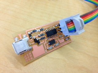
Shawn had also set up boards and a laser-cut stencil so we could try stuffing the boards using solder paste. We started by using the stencil and a silkscreening-type process to quickly spread solder paste over the entire board.
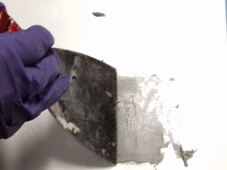
We then stuffed the board by placing the components in their positions and heating them in a reflow oven to melt the solder.
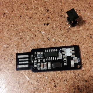
The result was much neater than the first board! It was also much more straightforward to program.
Finally, because my first attempt at the milling-and-stuffing process had been so messy, I wanted to work on those skills. So I made a second board using those techniques, this time with the "hello" ISP design. The entire process went much more smoothly the second time (so much so that I forgot to take pictures at each step...).
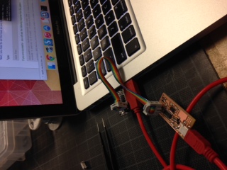
In the end, I was able to use one of the keys I had made and programmed to program the second milled board, which was really satisfying in a meta sort of way.
Jenny Kostka Fab Academy 2015
