Skulina Hlif Kjartansdottir
How to make [almost] anything
Week 6: Electronic Designs
This week we will learn more about electronic design processes. This is the agenda - we will be learning more about components, circuits and constructing boards with the eagle software and milling on the Roland Modela. We will also be learning about other relevant software and use of the fabmodules.org to machine the boards.
Week 6: Assignment
The assignment for this week is to redraw the echo hello-world board and to add a button and LED (with current-limiting resistor) to it, check the design rules, and make the board. An extra credit can be earned by simulating its operation.
We decided to make the hello.ftdi.44 circuit employing the eagle software for designing the boards.
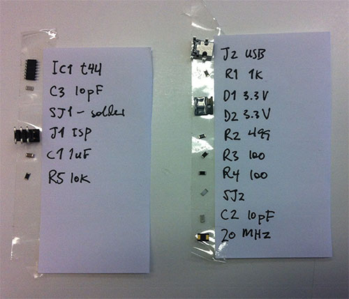
There exist some general guidelines on how to make circuites in the FabLab, that I studied. Information on the hello-world circuits can be sought here. I downloaded an eagle tutorial and studied guidelines for electronics design with eagle. The first task was to download eagle, to import a library (fab.lbr) and to position it in the eagle folder in documents. In eagle I started by making a new project, opening the schematic window and gradually add the relevant components. These were the components that I chose for the board.
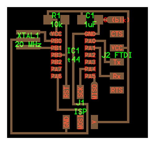
The components were dragged into the window and then arranged to be connected, according to the image of hello-world ftdi.44. I tried both the recommended ways of connecting, that is connecting with a wire and naming the nets according to the component that it needs to be connected to:
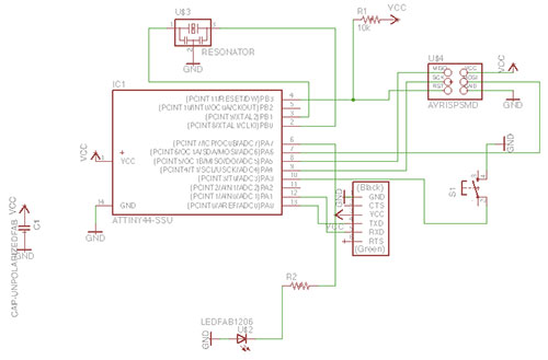
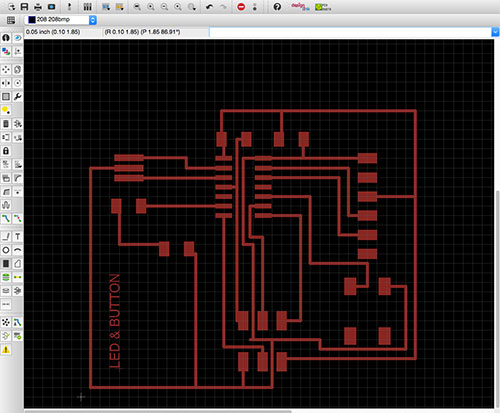
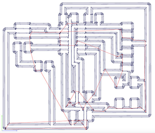
I then switched to the board view and started to route the traces of the board. First the components needed to be dragged into the frame. Then the “route” command was used to route between the components. Sometimes, when space was not sufficient, the “alt” button on the mac needed to be pushed in order to move in smaller steps and to find the most appropriate distance for clearance.
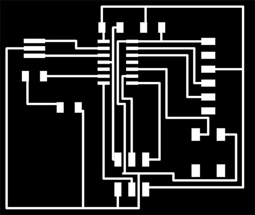
The process for saving and exporting the images in preparation for the milling of the boards is done in two steps, first the traces, an image with all components is created, then a square is drawn around the board circuits, approximately 1 grid line outside the square around it. The process is as follows:
When the board is defined the traces are exported. Before exporting turn off all layers except the top one.
The board image was exported as a monochrome image (. png, with resolution: 1200; image size: 2204 x 1860)- named: Hello-World-SHK.
For drawing the outline:
In layers – Select all – OK
In layers – Select bottom layer.
Chose - Rect, and draw a square around the board circuits – approx 1 grid outside the square around it.
It is possible to click info, double click the image and change the layer.
In layers – select 20 Dimensions – and export image as monochrome (resolution: 1200; image size: 2204 x 1810): Name of square / outline. The image was then opened in Photoshop and the square filled with white color.
I ran into trouble with some routes, that is their placement, when exporting the image did not give good traces. We had to go back to the design and adjust the clearance for Wire, Pad & Via and re-set the distance between the routes (from 0.40mm to 0.41mm). This seemed to solve the problem and the traces looked good for milling.
When the traces had been checked the milling could start. Checking the traces in fabmodules.org: insert image-png, set to Roland Mill (.rml) and PCB traces to 1/64. If the lines in the problem area are straight, and the correct number and connections seem to be ok then the board can be milled.
Start by cleaning the sacrificial layer and taping the board material on both sides. Glue the material for the board to the sacrificial layer. Check or change the tool to 1/64. In view go to home position and lower the tool. Change the xmin ymin numbers if neccessary. Move to xmin ymin and re-adjust the numbers if you have to. Then calculate and press send.
To cut the outline of the board, first press view and change the tool to 1/32. Then load the image – outline and set to Roland Mill (.rml) and outline - calculate. Press xmin ymin to bring the tool to the right starting position, then lower the tool to the surface of the board and fix its position. Calculate again and press send.
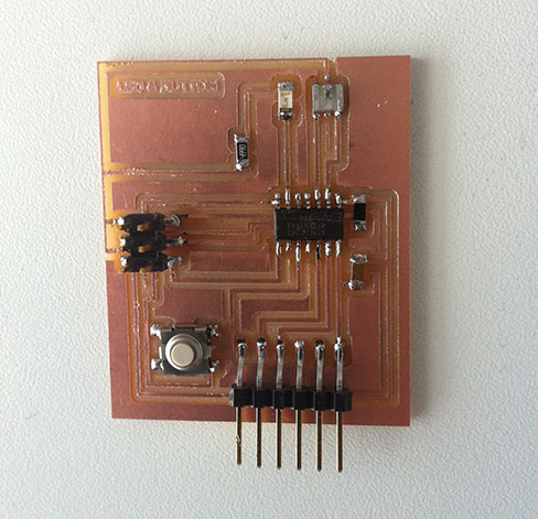
Finally all the components were soldered onto the board and the transmission of the current between VCC and Ground was tested with the digital multimeter. My board looks like this:
Plans for next Week
Do some reading upon electronics and circuits.
Notes
My Notes from this week.
Files
My Schematic File
My Board File