Skulina Hlif Kjartansdottir
How to make [almost] anything
Week 10: Input devices
This week we carrying on with electronics and learn about input devices. This is our agenda for the week.
Week 10: Assignment
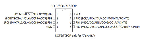
The assignment for this week is to to measure something: add a sensor to a microcontroller board that we've designed and read it. The microcontroller is a ATMEL 8 bit AVR programmable microcontroller and I used the ATtiny45/V for my board, which has 8 pins.
We can find useful information on different aspect of programming, such as the Py Serial documentation , Arduino references / tutorials and information on the individual components online.
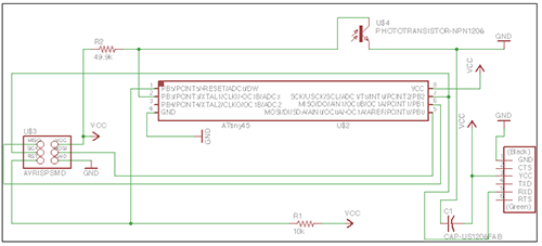
It is possible to measure various different inputs, such as sound, distance, movement, light etc. I decided to measure the input of light with a sensor and chose the Photoresistor 365-1481-1-ND for this task. A phototransistor uses light rather than electricity to cause an electrical current to flow from one side to the other. It is used in a variety of sensors to detect the presence of light. Other components were:
FTDI-SMD-HEADER = J2 FDTI
CAP-US = (CAP-US1206FAB – C1206FAB)
http://www.digikey.com/product-detail/en/C3216X7R1H105K/445-1423-1-ND/569089
RES-US = R1 10k (RES-US1206FAB – R1206FAB)
http://www.digikey.com/product-detail/en/RC1206FR-0710KL/311-10.0KFRCT-ND/731430
ATTINY45 = IC1 t45 microcontroller
http://www.digikey.com/product-detail/en/ATTINY45V-10SU/ATTINY45V-10SU-ND
RES-US = R2 49.9k (RES-US1206 – R1206)
AVRISPSMD = J1 ISP
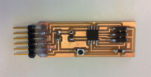
My input board was based on the Hello.light.45 board:
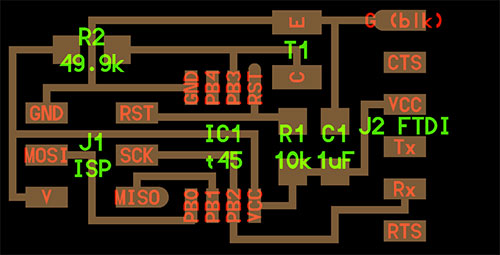
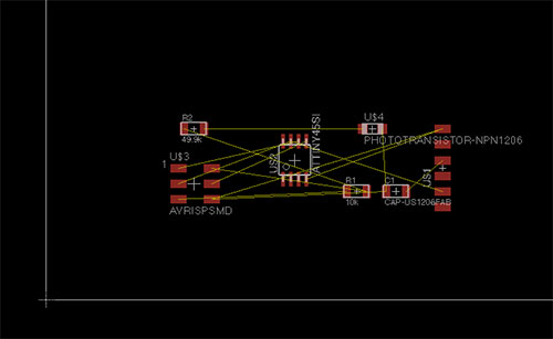
It was drawn in the eagle software. When all the components had been added in the schematic they were connected up.
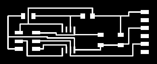
Then the connections of the board were drawn.
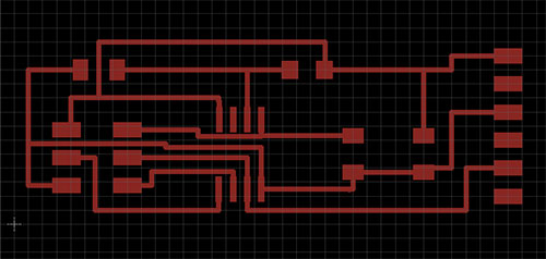
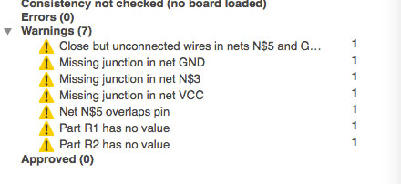
And error check was run which revealed problems of disconnection, clearance and overlaps that had to be mended.
Wires were drawn between component and components moved. Parts were given value. The ratnest tool was used to reveal the yellow helper lines to re-route them and export the files.
There were also some issues with density of lines, that were fixed later on the "traces" image in Phopshop, by defining the area and coloring with black to increase the space between connection lines. To remove text, if it was sticking out of the board: Edit smash – click on the + to remove text.
With the Group command I drew a square around the board from the upper left corner, right click and chose move group to move the whole board to the lower left corner. Then left click on the middle of contour line and drag the other corner to fit closely to the board.
In layers – Select all – OK. Again In layers – Select bottom layer.
Chose - Rect, and draw a square around the board circuits – approx 1 grid outside the square around it. Possible to click info, double click the image and change the layer. In layers – select 20 Dimensions.
Finally, both the "traces" and "interior" drawings were exported as a monochrome image (resolution: 1200; image size: 2204 x 810).
The milling of the board - workarounds. First tape board to table, Turn on machine – push view to move chuck to left end of working area. In fabmodules open the "traces" image. Select output format - Roland mill .rml. Process - PCB trace (1/64). Turn off view. Calculate.
Move ti xmin ymin. Adjust smin ymin settings – 2-2. If right – losen mill end and lower to surface of board. Check location of tool.
Send if ok. I encountered a bug in Fabmodules – because the old settings were still active it seemed, and the miling machine started cutting the following traces pattern.
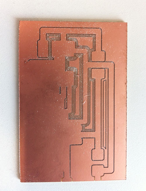
I therefore, had to reload the page and then the image and to adjust the cutting depth – from 1.0 to 1.5.
To cut the outline/interior, first press view and change the tool to 1/32. Then load the image – outline and set to Roland Mill (.rml) and ouline - calculate. Press xmin ymin to bring the tool to the right starting position, then lower the tool to the surface of the board and fix. Calculate again and press send.
I had some soldering issues that had be be corrected. I had to turn the photoresistor around and glue the FTDI in place, as it became unstable during the soldering process. This came to light during the programming process. I also checked the conductivity of the board, ground versus VCC (should not be a direct contact). I did a continuity test, measures resistance, but will beep if there is not resistance. My continuity test worked fine, as there was not sound, no direct contact. This is the appearance of the board.
The programming was done in Arduino. First I adjusted 3 settings. Board - ATtiny, Processor - 45, Clock - internal 8Mhz. This tells the programming environment how to behave. Now - Tools - burn bootloader. Next, the microcontroller needed to read the input from the light sensor (phototransistor). I used the AVR Programmer Hookup Guide to learn about programming the input and output pins of the microcontroller and checked the pin configurations.
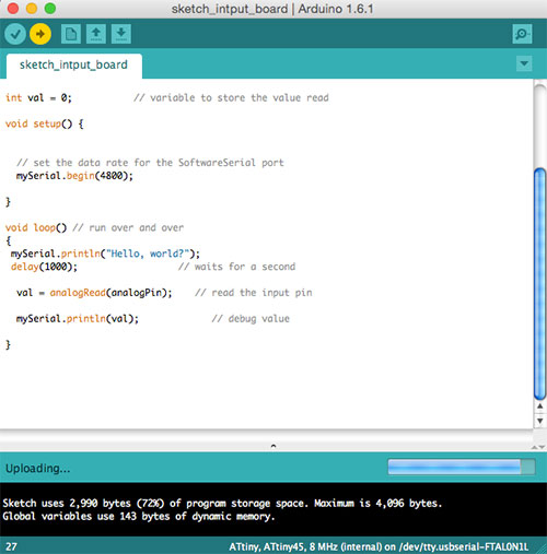
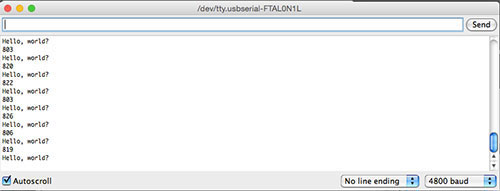
At first attempt to build and upload the program it did not work. The Serial Monitor window was emptly, the board was not sending anything. We took the board to testing in the Oscilloscope.
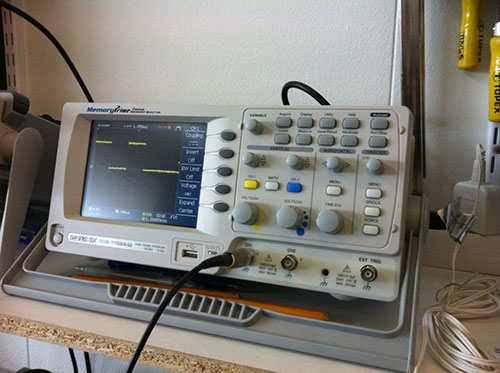
The testing revealed that the cause was that one pin on the FTDI was not working. It was resoldered and consequently we could confirm that the contact with the board was established. Reading hello world...and indicating the reading of the light input.
Plans for next Week
Study more programming and the Arduino references.
Notes
My Notes from this week.