7. Electronics design
This week I worked on defining my final project idea and started to getting used to the documentation process.
KICAD
This week I tried using Kicad. I found it a very difficult program to work with. I tried to redraw a hello world board and a LED and a push button but I some problems in the proces. The result was not what I expected. I tried to remake it after the first prototype but time was to short. I was not able to finish it in time.
I used this example to start with:
.png)
redraw the circuit in KICAD
I redrawed the circuit in KICAD and added the LED and push button. First I sellected the components and put them in the workplane. In the library of Kicad were a lot of components, because it was the first time i used this was very chaotic to find the right components.

I connected the components to eachother.

My colleague in the lab told me there was a mistake in the circuit with the push button so I redrawed the circuit.

When the circuit was finnished i had to add footprint too every components. This was the biggest problem because the library was gigantic.


I didn’t find every component in the library, so i guessed the right ones. but ater i milled the board I saw that it was to big for the smd components.
The last step in KICAD was drawing the paths for the PCB. This was the most clear part of the assigment. I enjoyed this part because it was the most concrete part of the assigment.


I choose the plot option to export the files i need for the milling part.


The milling I did the same way i did 2 weeks ago in the electronic production assigment.
When the milling was ready i realised that the board was to big for the components. I tried to solve this problem by soldering bigger componenst on the board with the same values, but for the Attiny it was a big problem.

components
i Used the following components on the board. (i) LED; (ii) three resistences (470, 1k, and 10k); (iii) capacitor of 1µf. It was used a button with four connections (although they are mirrored). ATtiny45. The jumper ISP-6 used was folded ones and the FTDI was normal jumpers (4 pins).
programming the board
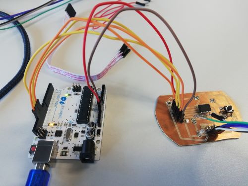
After I milled the new board I soldered the components on it.

When this wa done i tried to program it with the programmer but this didnt work so i dit it with the arduino as isp. I connected the hello world to the arduino. I uploaded blink to see if the board was working. I changed the output from PB1 to PB3 because the led is on this pin of the attiny.
- GND —> GND
- PB2 —> SCK —> D13
- PB1 —> MISO —> D12
- PB0 —> MOSI —> D11
- Reset —> D10
- VCC —> 5v
blink code :
We used this code to to check everything. This code blink the LED each second. I used the function delay(1000), it receives the time in miliseconds. The variable LED was added to point to the ATtiny pin of the LED. The function digitalWrite changes the state of the pin to HIGH or LOW, respectivelly has electricity or not.
``` ” int LED = PB3;
void setup() { // initialize digital pin LED_BUILTIN as an output. pinMode(LED, OUTPUT); }
// the loop function runs over and over again forever void loop() { digitalWrite(LED, HIGH); // turn the LED on (HIGH is the voltage level) delay(1000); // wait for a second digitalWrite(LED, LOW); // turn the LED off by making the voltage LOW delay(1000); // wait for a second ”
then i added the push button.
int pshbutton = PB4; int LED = PB3;
void setup() { // put your setup code here, to run once: pinMode(pshbutton, INPUT_PULLUP); pinMode(LED, OUTPUT); }
void loop() { // put your main code here, to run repeatedly: if (!digitalRead(pshbutton)) digitalWrite(LED,HIGH); else digitalWrite(LED,LOW); }
```
setting the arduino


I uploaded the adjusted blink code and the led started blinking.
downloads
### link the the group assigment electronic design