- Circuit Design & Board Design at EAGLE
1. Weekly Brief Summary
I used EAGLE to create a schematic diagram based on the breadboard circuit for the earrings and banding. Next, I used sketches to validate the board design and the structure of the device, and then I used EAGLE to design the board from this.
2. Description of Assignment Work
Earring side
Based on the breadboard circuit we created, we selected surface-mounted sensors and other components to be used.
breadboard diagram
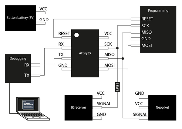
① ATtiny85
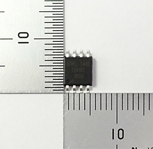
The ATtiny85 decided to use a surface-mounted [AVR microcontroller ATTINY85-20SUR].
data sheet
-
Main Specifications
| Function | Details |
|---|---|
| Power supply voltage | 2.7~5.5V |
| core size | 8bit |
| clock | 20MHz |
| GPIO | 6 pin |
footprint
I used [TINY25/45/85-20SU] in [avr-7].
② IR Receiver
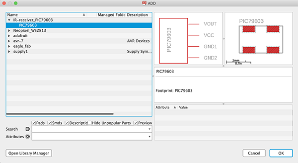
I decided to use a surface-mounted [[Remote Control Receiver Module PIC79603]] (http://akizukidenshi.com/catalog/g/gI-11734/) for the IR receiver.
data sheet
- Main Specifications
| Function | Details |
|---|---|
| Power supply voltage | 2.7~5.5V |
| Current consumption | 0.9~1.3mA |
| Peak Sensitivity Wavelength | 940nm |
| Tuning frequency | 37.9kHz |
footprint
I couldn’t find the footprint of [PIC79603] on the web, so I used EAGLE to create my own [IR-receiver_PIC79603.lbr].(specified in → [Creating symbol & footprint data for the device to be used])
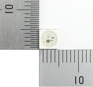
③ Neopixel
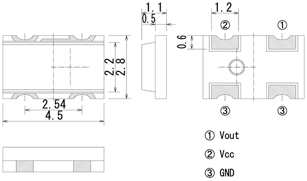
Neopixel decided to use the surface-mounted [RGB LED WS2813B with built-in microcontroller].
data sheet
- Main Specifications
| Function | Details |
|---|---|
| Power supply voltage | 5V(3.5V~5.3V) |
| LED | RGBLED |
| Red | 620-625nm 360mcd |
| Green | 515-525nm 1150mcd |
| Blue | 465-475nm 220mcd |
footprint
I couldn’t find a footprint for [WS2813B] on the web, so I made my own [Neopixel_WS2813.lbr] using EAGLE.
④ 33kΩ
For 33kΩ, I decided to use a surface mount [Chip Resistor 1/10W33kΩ].
datesheet
footprint
I used [R1206FAB] in [eagle_fab.lbr].
⑤ 0.1μF
I decided to use surface mount [Chip Monolithic Ceramic Capacitors 0.1μF100V C0G 3216] for the 0.1μF.
datesheet
footprint
I used [C1206FAB] in [eagle_fab.lbr].
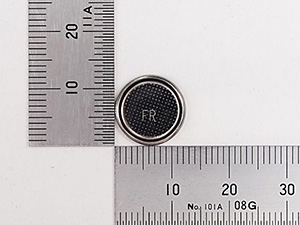
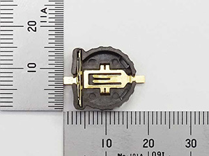
⑥ Battery
I decided to use [Lithium battery CR1220 from Golden Power] for Battery. And I used [Holder for Button Cell Substrate for CR1220 CH291-1220LF] for the battery holder.
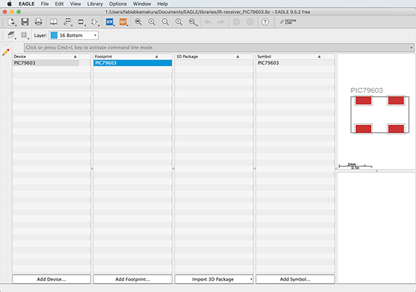
Creating symbol & footprint data for the device to be used
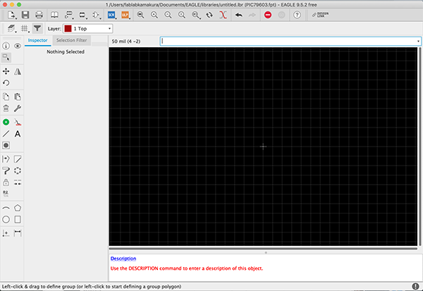
I couldn’t find the symbol & footprint data for [Remote Control Receiver Module PIC79603] on the web, so I used EAGLE to create the data myself.
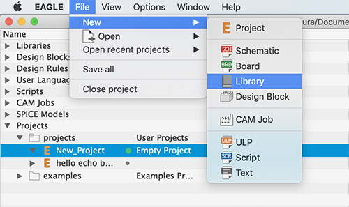
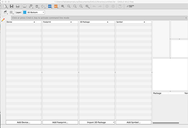
(1) Create a parts library in EAGLE
With EAGLE, it is necessary to store all the parts you have created in the “Library”. Even if you only have to create one part, you must always create a library.
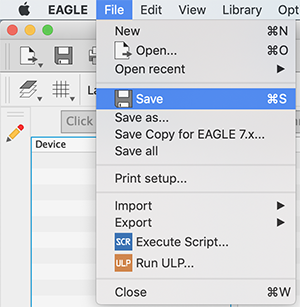
You can create a new part library from [File] - [New] - [Library].
Create a new library from the EAGLE start page.
The basic page of the EAGLE library. Use this page as a basis for editing symbols, footprints, 3D data, etc.
It can’t save it by just creating a new Library, so I should save it once in this screen. Save the file with a name that is easy to distinguish.
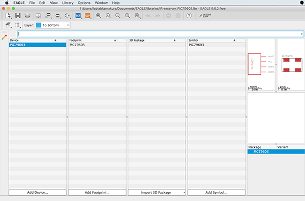
(2) Adding a part name to the parts library
After creating the part library, you can proceed to create the part. In the Device, where you specify the part name, the symbol, footprint and 3D model associations, as well as the wiring information and part prefix information are stored.
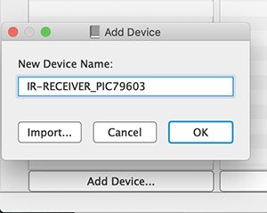
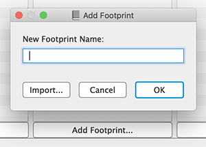
[Add Device…] in the [Device] bar on the left side of the screen and enter the product name of the part you want to register.
Click the [Add Device…] button at the bottom left to register the part name. Enter a product name that is easy to understand and press OK button.
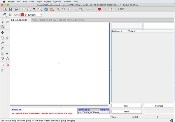
When the registration of the parts is finished, the screen to link the parts opens. Press the “Table of contents” button on the upper left to go back to the previous screen.
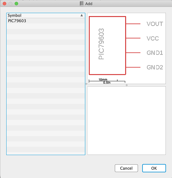
(3) Create a [part symbol]
A parts symbol is a circuit symbol that appears on a circuit diagram. However, in many cases, a new symbol must be created when a special switch or microcontroller is included in a circuit diagram.
There are two main ways to create a part symbol, one is to create it from scratch and the other is to import it from another library.
In this article, we will use the “Create from scratch” method, but it is rarely necessary to create the actual symbol from scratch. In general, you can import other part symbols and adjust their shapes.
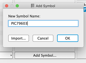
Press “Add Symbol…” at the bottom right to decide the name of the symbol. It doesn’t have to be the same name as the part we are adding, so we have to give it a name that is easy to recognize.
Symbol Editor opens. In this screen, make the shape and terminal of the electronic circuit. To make a rough shape, draw a shape or a line from the left menu.
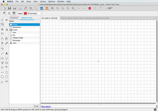
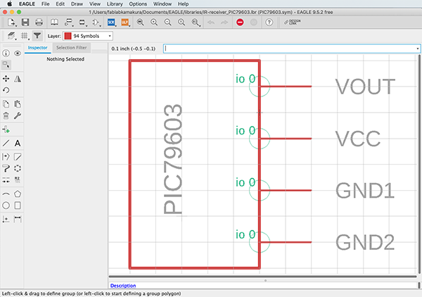
Making the PIC79603 symbols. I created a rough shape based on the PIC79603 datasheet.
It will take some time to get used to the unique way of operating it. The basic way to use this application is to adjust the position of roughly created shapes and lines by entering the coordinates.
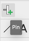
Once the overall shape is complete, set up the connection terminals. Select the “Pin” button from the left menu.
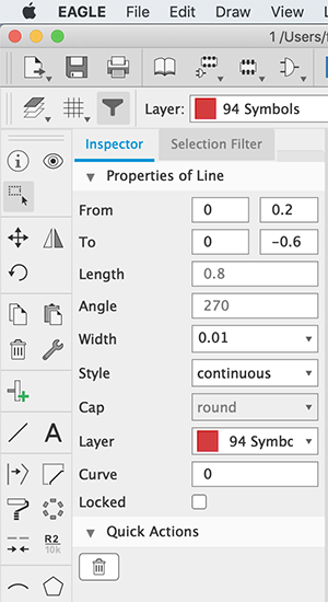
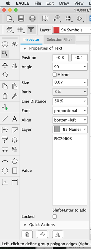
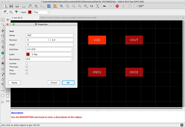
When a placed pin is selected, the shape of the pin can be adjusted from the Inspector menu. Rotation is adjusted by [Angle] element, length of pin is short by [Length] element. In this case, we don’t need the pin name, so we turn off [Visible] element.
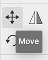
To move the pin, select [Move] from the left menu and click the pin in the move state.
This is a completed symbol, but when we place it in the schematic, it doesn’t indicate the quantity (L1, L2) and capacity of the parts. In the end, we need to specify [Text] to indicate the quantity and capacitance.
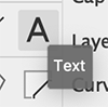
In Text, enter [>NAME] and specify [Layer] as 95 Names. With this setting, part numbers with prefixes such as L1, L2, etc. will be displayed automatically.
Save it when completed.
(4) Create a [footprint]
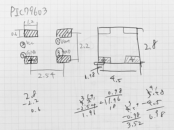
The next step is to create a footprint. In creating the footprint, we referred to the electronic component data sheet to create it. The datasheet includes a “Recommended Pattern Diagram” which we used to create the pattern.
Select [Add Footprint…] at the bottom of the screen to create a new footprint.
The screen to create a footprint.
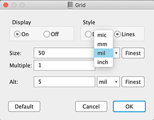
Since the dimensions are in inches, change the unit to mm to conform to the data sheet. You can change the unit from [Gred] menu.
Select [Smd] to connect the terminal and the contact. Select [Hole] for axial components.
One of the [Smd] was set to the origin.
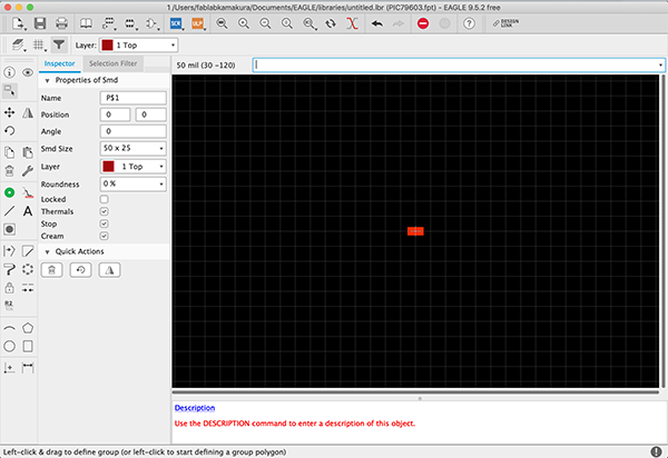
I calculated the positions of the other [Smd] from the origin by myself, referring to the recommended pattern diagram.
↓
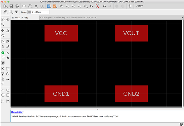
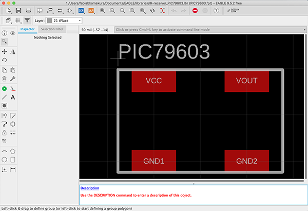
Assigned a function to each [Smd].
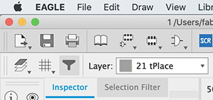
I need to set up a silk pattern to represent the position and information. Change [Layer] to tPlace and choose [Line] from the left menu.
Infine, aggiungere [>NOME] nello stesso modo della procedura dei simboli. Utilizzare [Text] per posizionarlo nella posizione migliore e cambiare [Layer] in tNames.
(5) Associare i nomi delle parti con impronte simboliche
Once you have completed this step, the final step is to associate the symbol with the footprint. In this step, we will link the symbol’s terminals to the contacts of the footprint and specify the comments and prefixes of the parts.
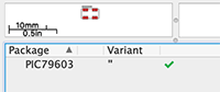
Select and open the device you created in step (1).
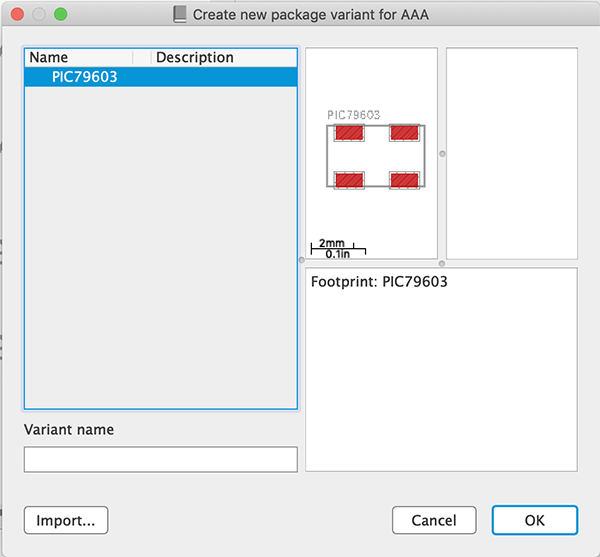
Place the symbol created in (2) from the [Add Part] button on the left.
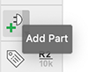
The Add window displays the symbols that were stored in the library. Specify them and press OK.
↓
Next, specify the footprint. Select [New] on the right and then [Add local package].
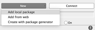
The Add window shows the footprints stored in the library. Specify them and press OK.
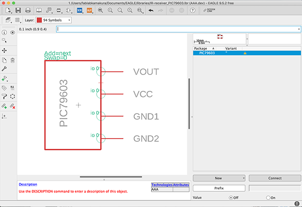
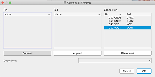
After placing the symbol and foot pattern, connect the terminals and contacts. Press the right [Connect] button.
In the [Connect] window, the symbol’s terminal and footprint contacts are shown, select the function to be connected and press the [Connect] button in the lower left corner.
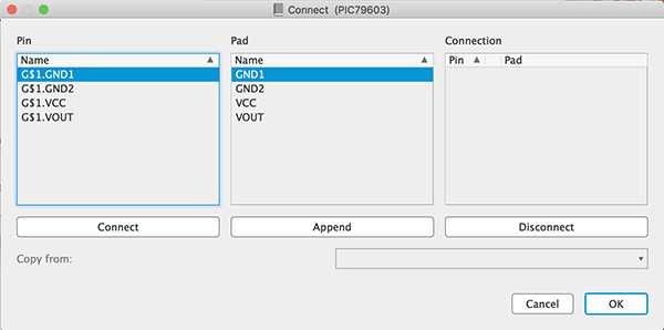
Match all the connectors together and it’s done. Now it will work as a homemade part.
↓
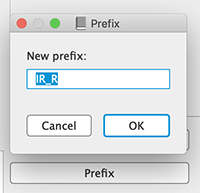
You can use it as it is, but you must specify the prefix of the parts at the end. Push the “Prefix” button at the bottom right. Since this part is an IR receiver, enter “IR_R” and press OK. Now every time you add a new part, it is automatically assigned a part number: IR_R1, IR_R2, IR_R3,,, etc.
Now you can use the symbol & footprint data of [Remote Control Receiver Module PIC79603] in EAGLE.
Consideration of board design
Before I created [Schematic] in EAGLE, I considered the design of the board to be produced.
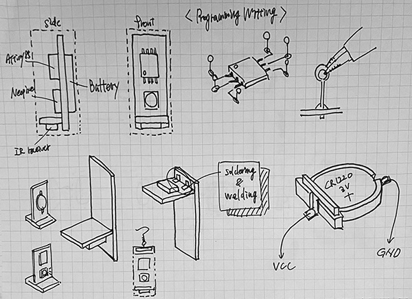
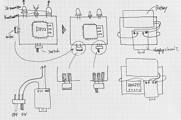
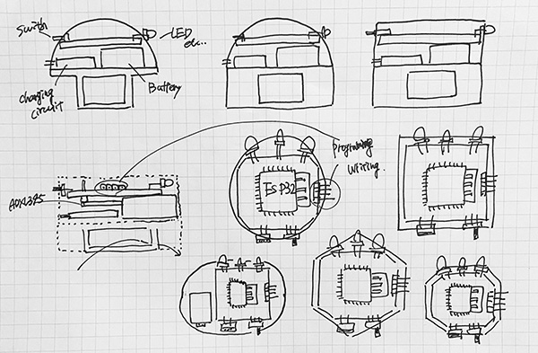
For this project, I came up with a mechanism to vertically connect two [substrate B], [substrate A] with [ATtiny85], [Neopixel], and [Battery] in place, and [substrate B] with [IR receiver] in place. So we decided to weld the two boards together during the soldering process. In order to design the boards as small as possible, we also decided to use tin-plated wire to fabricate pins for writing programs, and then drill holes in the boards and weld them together.
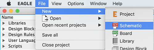
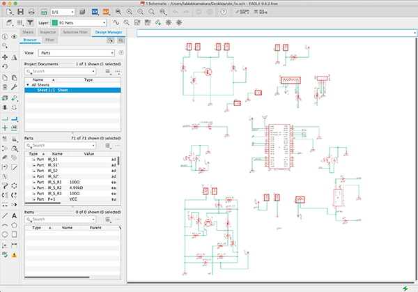
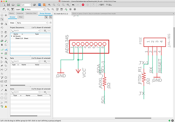
Creating a [Schematic]
I was able to prepare the symbol and footprint data for the parts used on the earring side, so I created a schematic in EAGLE.
From the menu, [FIle] → [New] → [Schematic] to open the new data.
Click the [Add Part] button on the left to open the list of parts and place the parts you want to use.

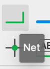
I used the [Net] tool to wire up the placed components.
↓
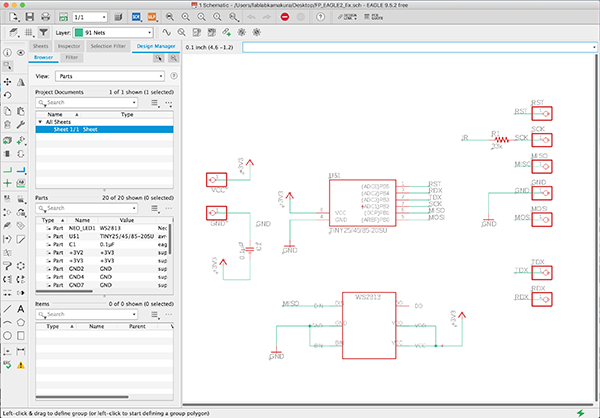
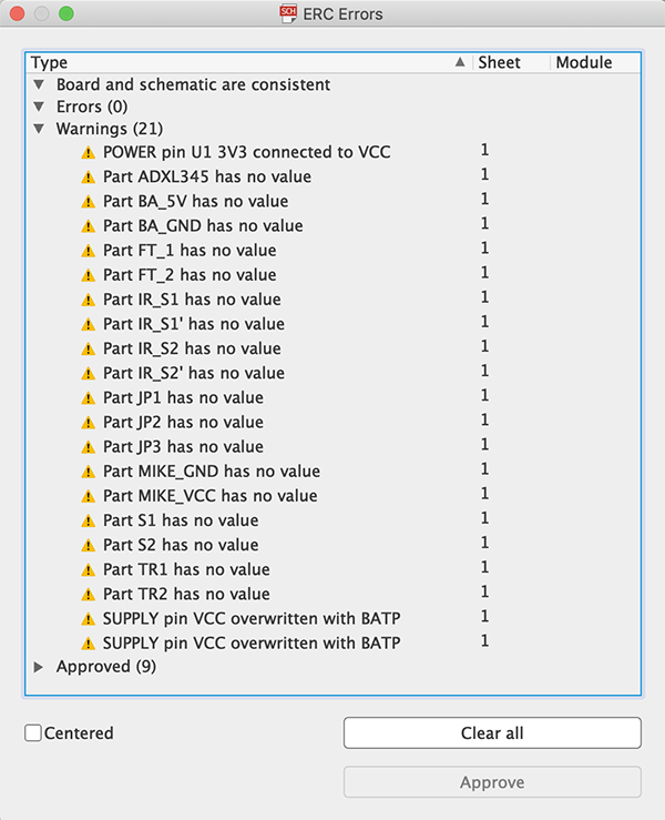
After wiring was completed, I used the [Electrical Rule Check] tool to check the wiring between components.
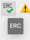
The warning [Part xxx has no value] is displayed, but I ignored it because it’s not necessary to make the board I’m going to create this time.
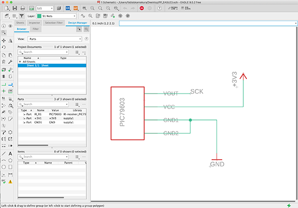
Lastly, I created a schematic for the infrared receiver side. Since this board is for welding, I will design it so that it will connect to the other board after I make the board diagram.
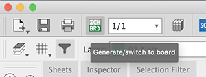
Creating the [Board]
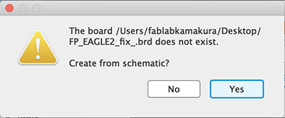
Click the [Generate/switch to board] button at the top of the schematic window to move to the creation screen.
At first you will be asked if you want to generate it automatically from the schematic because there is no corresponding board diagram (.brd) file. Click the [Yes] button.
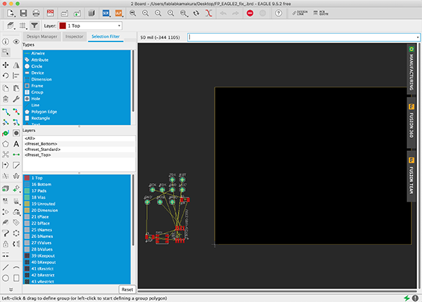
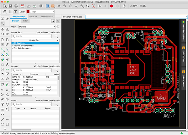
The board diagram was automatically generated, and I placed the components placed on the left side of the frame, keeping them close to the board structure I was considering.
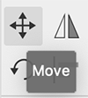
With the [Move] icon selected, we clicked on the part to be moved, moved it and then clicked again to place it. You can rotate the part by right-clicking while the part is selected.
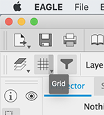
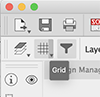
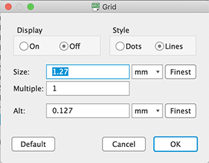
Set the unit of measurement in [mm] for moving the frame line by clicking the Grid button in the upper left corner.
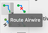
After placing the components, use the [Route Airwire] to connect the components together.
Before that, I clicked the Grid button and changed the unit to inches to set the solid color. Then I set the width of the solid color to [0.016] and connected the wires.

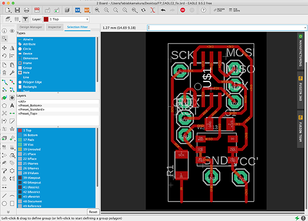
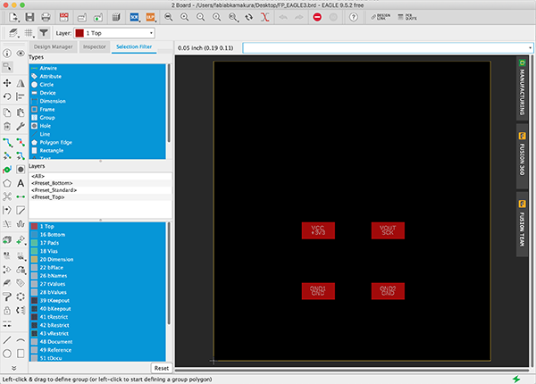
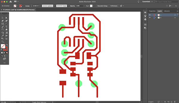
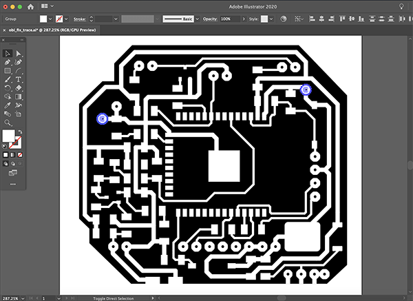
The final board design for [Board A] looked like this.
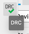
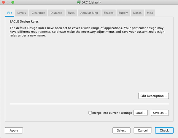
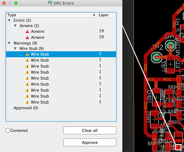
I used [DRC] to check that the board was designed in accordance with the design rules of board manufacturing, such as spacing between wires.
Click the [DRC] button at the bottom left of the Bode diagram window to display the DRC setting menu.
↓
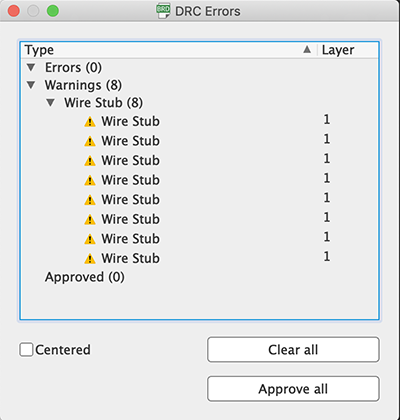
When I clicked the [Check] button, a window displaying the list of errors will appear. The warning “Wire Stub” is displayed, but I ignored it because it is not necessary to make the board that I will make this time.
That’s all we have to do for [Substrate B] in EAGLE. We create the pattern in accordance with the design of [Substrate A] created earlier using [Adobe Illustrator].
Exporting a Pattern Diagram
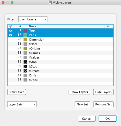
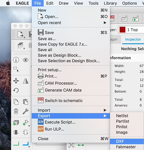
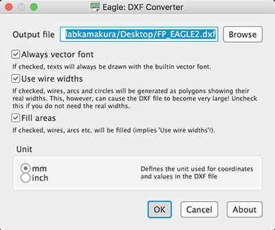
Export the created [Board A] and [Board B] designs as a [DXF] file in order to edit them in [Adobe Illustrator]. Make only [Top] and [Pads] of [Used Layers] visible when exporting. Note that if you make other layers visible, their data will be output as well.
I selected [File]→[Export]→[DXF], made sure that the unit was set to [mm], and saved it on the desktop.
Corrections in [Adobe Illustrator]
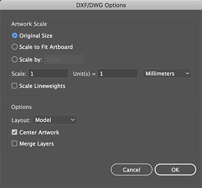
Open the [DXF] file of [Board A] exported by [File]→[Open] by [Original Size].
↓
The solids and pads were the color on the EAGLE.
↓
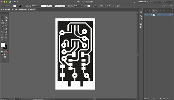
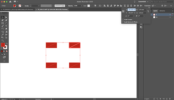
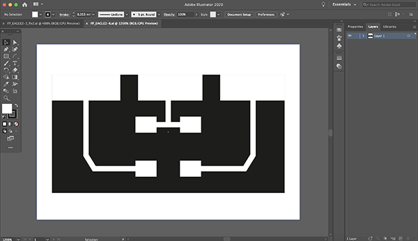
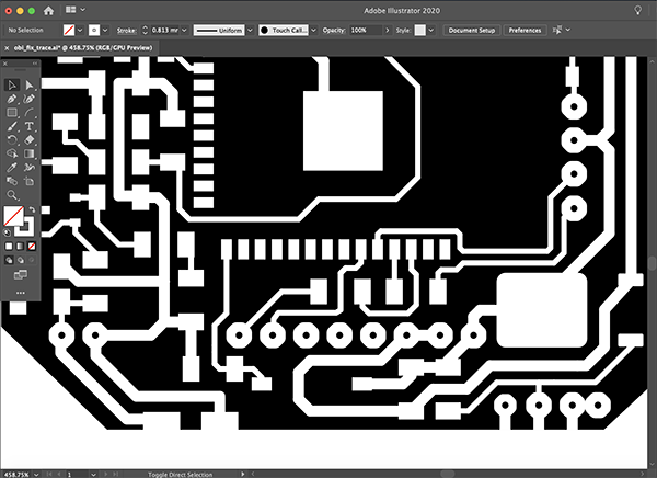
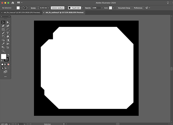
The solid and pad areas and other non-cutting areas were made in white and the rest of the area was made in black. The pads are drilled after the cutting process, but the size of the hole is too large for the end mill on the cutting machine, so I created marks for later machining. I also created a larger pad for the area to be welded to [substrate B].
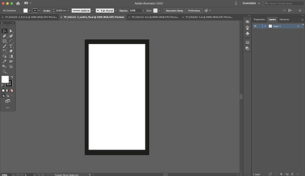
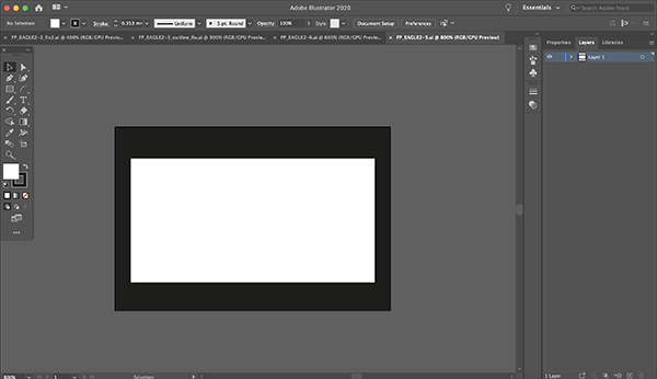
The outline data of the board was then created.
I finished making both the pattern and outline data and exported them in [PNG] format.
Similarly, I opened the [DXF] file of [Substrate B] in [Adobe Illustrator] and created a pattern drawing and outline data.
↓
The center pad is connected to [GND] and the left and right pads are connected to [VCC].
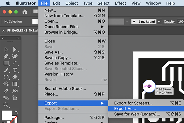
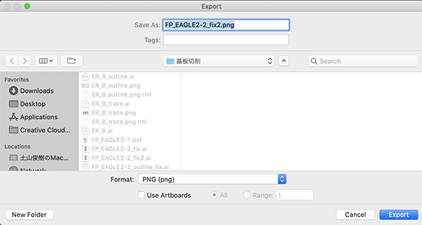
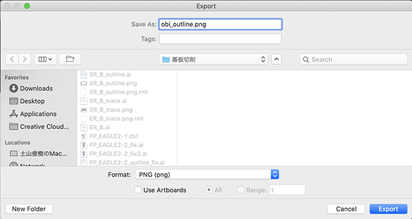
I exported the pattern and outline data as a [PNG] file. First, select [File]->[Export]->[Export As…] Select [File]->[Export]->[Export As…].
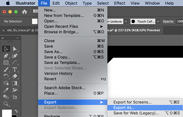
Choose [Format] to [PNG(png)] and click [Export].
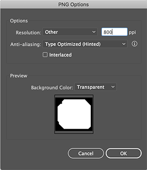
In the [PNG Option], set the resolution to [800dpi] and click [OK]. This is necessary to generate G-code in Mods.
Obi clasp side
Based on the breadboard circuit we created, we selected surface-mounted sensors and other components to be used.
breadboard diagram
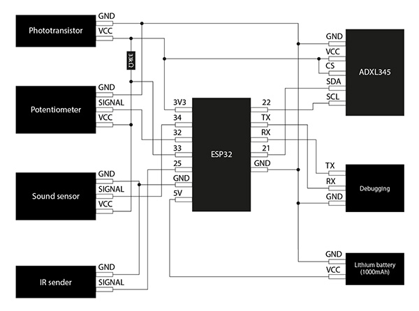
① ESP32
I decided to use the surface-mounted Wi-Fi module ESP-WROOM-32 for the ESP32.
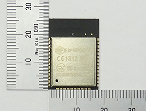
data sheet
- Main Specifications
| Function | Details |
|---|---|
| Power supply voltage | 2.2V~3.6V |
| SRAM | 520KB |
| WiFi | 802.11 b/g/n |
| Bluetooth | v4.2 |
I also have some new components based on [Barduino 2.0], which implements the ESP32. When writing a program to the ESP32 using an Arduino, when you see [Connecting…], press the reset button and when you see [Leaving… Hard resetting via RTS pin], press the switch Switch to run mode and press the reset button. So you need two [tact switch], which is necessary to write the program.
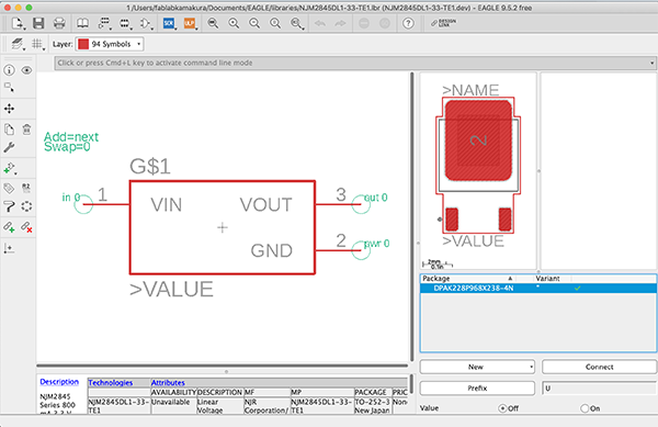
In addition, a regulator [NJM2845DL1-33] is available to control the output voltage and current so that it is always constant.
data sheet
Finally, we have an LED for the ESP32 debugging.
- Parts used
| Function | Details | Number |
|---|---|---|
| ESP32 | Wi-Fi module ESP-WROOM-32 | 1 |
| Switch | tact switch | 2 |
| Regulator | NJM2845DL1-33 | 1 |
| LED(Red) | Red Chip LED [1608] OSHR1608 | 1 |
| Resistor ⑴ | 100Ω | 2 |
| Resistor ⑵ | 10kΩ | 2 |
| Resistor ⑶ | 2.2kΩ | 2 |
| Capacitor ⑴ | 0.1μF | 2 |
| Capacitor ⑵ | 10μF | 2 |
| Programming Writing | 4 pin header | 1 |
Footprint
I used [ESP-WROOM-32], which is in [ESP32.lbr]. I couldn’t find the regulator footprint on the web, so I made my own using EAGLE, using the datasheet as a reference.
I used [TACT_SWITCH] in [fab.lbr] for the TACT switch footprint and [LEDFAB1206] in [eagle_fab.lbr] for the LED(Red) footprint. I also used [R1206FAB] in [eagle_fab.lbr] for the resistor footprint and [C1206FAB] in [eagle_fab.lbr] for the capacitor. I decided to use a 4-pin pin header to write the program, so I used four [PINHD-1×1] in [adafruit.lbr] for its pads.
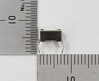
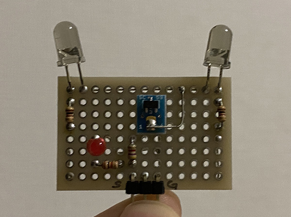
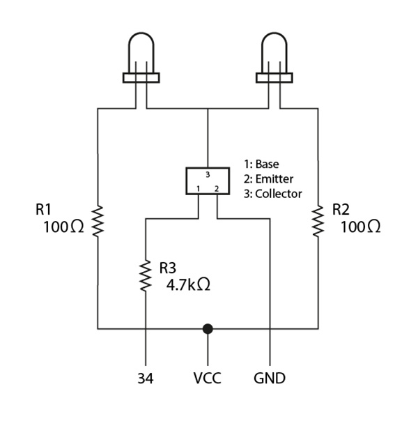
② Infrared Transmitter
For the infrared transmitter, we decided to use a partial switch from the device used for the breadboard circuitry to a surface mount component.
schematic
- Parts used
| Function | Details | Number |
|---|---|---|
| Infrared Transmitter | 5mm Infrared LED 940nm OSI5LA5453B | 2 |
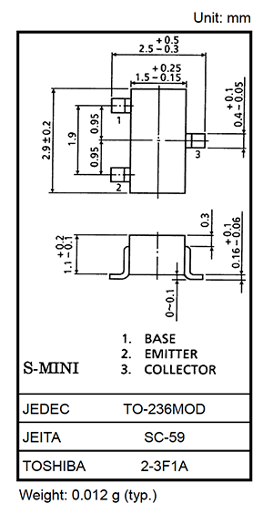
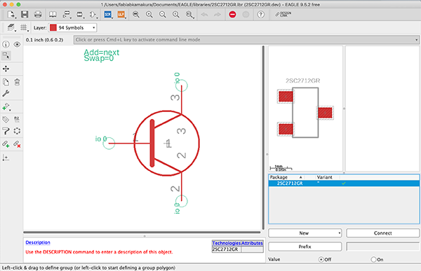
| Chip transistor | 2SC2712-GR | 1 |
| Resistor ⑴ | 100Ω | 2 |
| Resistor ⑵ | 4.7kΩ | 1 |
Footprint
I couldn’t find a footprint for the [2SC2712-GR] on the web, so I made my own using EAGLE, using the datasheet as a reference. I also used [R1206FAB] in [eagle_fab.lbr] for the resistor footprint and [PINHD-1×1] in [adafruit.lbr] for the LED pads.
data sheet
↓
③ Phototransistor
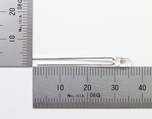
Phototransistor [Phototransistor 3mm round type 940nm L-31ROPT1C] used for breadboard circuit.
dateseet
- Main Specifications
| Function | Details |
|---|---|
| short legs | collector(C) |
| long legs | emitter(E) |
| feature | ・It has a large lens and high sensitivity. ・Fast response time. |
- Parts used
| Function | Details | Number |
|---|---|---|
| Phototransistor | Phototransistor 3mm round type 940nm L-31ROPT1C | 1 |
| Resistor | 33kΩ | 2 |
footprint
I used [R1206FAB] in [eagle_fab.lbr] for the Resistor footprint and [PINHD-1×1] in [adafruit.lbr] for the LED pads.
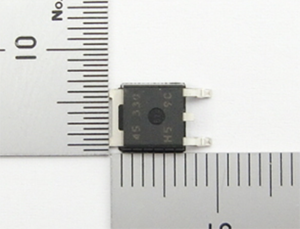
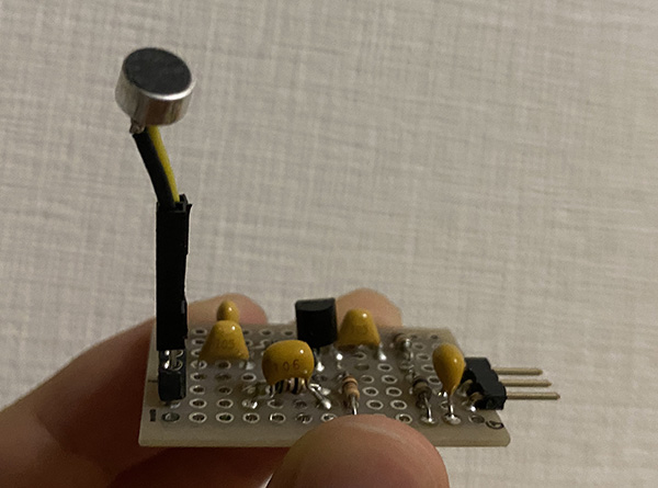
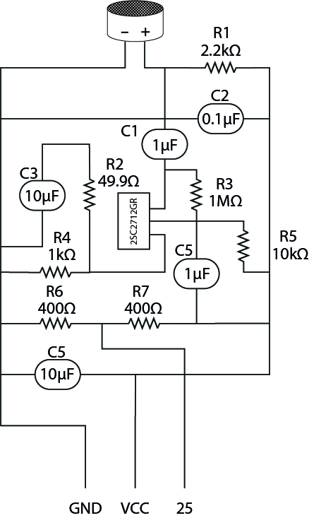
④ Sound Sensor
For the sound sensor, we decided to use a partial switch from the device used for the breadboard circuitry to a surface mount component.
schematic
- Parts used
| Function | Details | Number |
|---|---|---|
| Microphone sensor | [Electret Condenser Microphone (ECM) WM-61A or equivalent with lead pin] | 1 |
| chip transistor | 2SC2712-GR | 1 |
| Resistor ⑴ | 400Ω | 2 |
| Resistor ⑵ | 49.9Ω | 1 |
| Resistor ⑶ | 10kΩ | 1 |
| Resistor ⑷ | 1MΩ | 1 |
| Resistor ⑸ | 1kΩ | 1 |
| Resistor ⑹ | 2.2kΩ | 1 |
| capacitor ⑴ | 0.1μF | 1 |
| capacitor ⑵ | 10μF | 2 |
| capacitor ⑶ | 1μF | 2 |
footprint
I made my own [2SC2712-GR] footprint, [R1206FAB] in [eagle_fab.lbr] in the Resistor footprint, [Electret Condenser Microphone (ECM) WM-61A or equivalent with I used [PINHD-1×1] in [adafruit.lbr] for the [lead pin] pad.
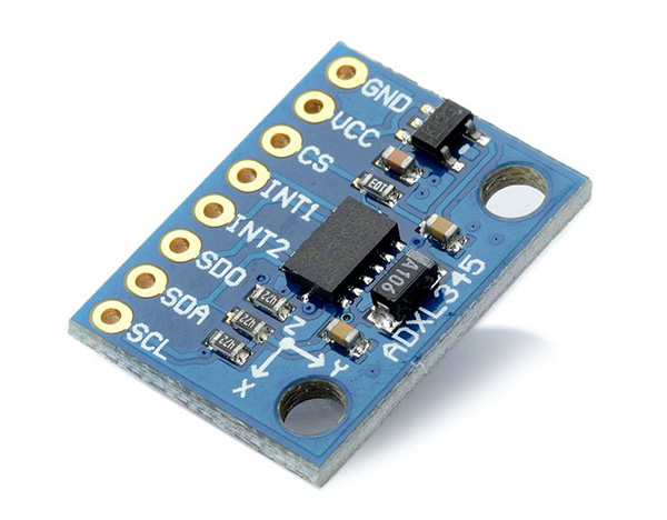
⑤ Accelerometer ADXL345
I decided to use the [ADXL345] used for the breadboard circuitry as it is for the Accelerometer.
data sheet
- Parts used
| Function | Details | Number |
|---|---|---|
| Accelerometer | ADXL345 | 1 |
| Connect | 6 pin header | 1 |
footprint
I decided to use a 6-pin pin header to plug the ADXL345 directly into the board. So I used the [PINHD-1×6CB] in [adafruit.lbr] for that pad.
⑥ Power Supply
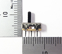
I used [Rechargeable lithium battery(1000mAh)] and charging circuit [Lithium Ion Charging Module_TP4056] for breadboard circuit. And I used Slide switch for boards SS-12D00-G5 as a power switch.
dateseet
footprint
I decided to create the footprint of the slide switch in [Adobe Illustrator] instead of EAGLE as I did when I created the pattern diagram for the infrared receiver in [Board B].
Consideration of board design
Before I worked on EAGLE, I considered the design of the board to be produced. When you look at the device from the front, you must place the infrared transmitter and phototransistor at the top. Then I thought it would fit together as a design by placing the microphone sensor, power switch, and charging circuit underneath the device so that it could be operated.
The device was originally going to be a round design, but we felt that we needed to consider a square or hexagonal design due to the space available on the board. We don’t plan to make the device itself too large, but rather we want it to be less than 700mm in width and length, and less than 500mm in height.
Creating a [Schematic]
I was able to prepare the symbols and footprint data for the parts used on the obi-dome side, so I created a schematic using EAGLE.
The warning [Part xxx has no value] is displayed, but I ignored it because it’s not necessary to make the board we’re going to create this time.
Creating the [Board]
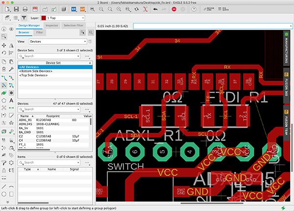
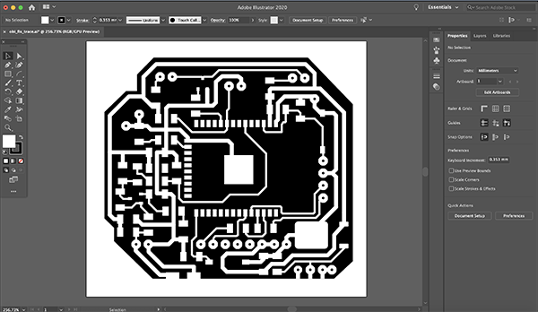
The next step is to create the board diagram. The final board design for [Board B] looks like this.
This time, unlike [Board A], the width of the solid bars connected to the power supply such as GND and VCC is set to [0.032] inch. This treatment is to make the resistor value low.
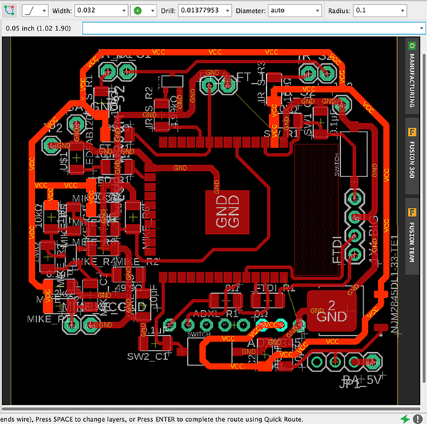
Also, since there were quite a few parts to be used in this project, there were parts that could not be connected. I thought about using [0kΩ] to connect wires by passing a solid underneath the components. So I added [0kΩ] in the [Schematic] section.
↓
Lastly, I used the [DRC] to check the spacing between the wires. There are some parts of the pattern that are not connected, but this is not a problem as I used tin plated wires to connect these parts.
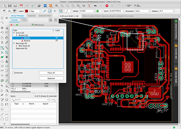
I also found 9 extra solids in [Wire Stub], but I ignored them as they were warnings that I didn’t need to worry about, especially when exporting the pattern diagram as an image.
Corrections in [Adobe Illustrator]
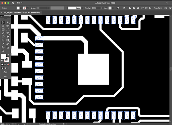
I edited the [DXF] file exported by EAGLE in the same way as [Substrate A] by using [Adobe Illustrator]. In the final pattern, I reduced the extra space as much as possible and made the corners as small as possible.
What I modified here is the size of the footprint of the ESP32…the footprint is too wide to be machined with the pattern created by EAGLE, so I made a [0.016]-inch space for a solid block.
The device was originally going to be a round design, but we felt that we needed to consider a square or hexagonal design due to the space available on the board. I don’t plan to make the device itself too big, but we want it to be less than 700mm in width and length, and less than 500mm in height.
The part you are selecting is the part where you drill a hole and connect the wires from the back with tin-plated wire.
Finally, I created the outline data. I exported the pattern and outline data in the [PNG] file format.
3. Links to Files and Code
Footprint
- avr-7(ATtiny85 etc…) [lbr]
- IR receiver(PIC79603) [lbr]
- Neopixel(WS2813B) [lbr]
- eagle_fab(Resistor etc…) [lbr]
- fab(tact switch etc…) [lbr]
- adafruit(pin header etc…) [lbr]
- esp32 [lbr]
- NJM2845DL1 33 TE1 [lbr]
- 2SC2712GR [lbr]
- supply1(GND/VCC etc…) [lbr]
EAGLE date
- Earring [sch]
- Earring [brd]
- Infrared receiver [sch]
- Infrared receiver [brd]
- Obi clasp [sch]
- Obi clasp [brd]
PNG file
- Earring trace date [png]
- Earring outline date [png]
- IR receiver trace date [png]
- IR receiver outline date [png]
- Obi clasp trace date [png]
- Obi clasp outline date [png]
![[png]](../../finalproject/files2/earring_trace.png)
![[png]](../../finalproject/files2/earring_outline.png)
![[png]](../../finalproject/files2/IR_trace.png)
![[png]](../../finalproject/files2/IR_outline.png)
![[png]](../../finalproject/files2/obi_trace.png)
![[png]](../../finalproject/files2/obi_outline.png)