Embedded Programming
First, read the Attiny45 datasheet and then, program our HelloBoard with as many languages as possible. The datasheet is very important, to know the functions of each pin, working voltages...before starting to work with a component, it´s needed to at least know where is the datasheet to consult when a doubt appears.
Datasheet
The ATtiny 45 provides the following features:
- 1. 4K bytes of In-System Programmable Flash
- 2. 256 bytes EEPROM
- 3. 256 bytes SRAM
- 4. 6 general purpose I/O lines
- 5. 32 general purpose working registers
- 6. One 8-bit Timer/Counter with compare modes
- 7. One 8-bit high speed Timer/Counter
- 8. Universal Serial Interface, Internal and External Interrupts
- 9. A 4-channel, 10-bit ADC, a programmable Watchdog Timer with internal Oscillator, and three software selectable power saving modes.
- 10. CPU and all I/O modules except ADC, to minimize switching noise during ADC conversions.
- 11. The device is manufactured using Atmel’s high density non-volatile memory technology. The On-chip ISP Flash allows the Program memory to be re-programmed In-System through an SPI serial interface, by a conventional non-volatile memory programmer or by an On-chip boot code running on the AVR core.
- 12. The ATtiny 45 AVR is supported with a full suite of program and system development tools including: C Compilers, Macro Assemblers, Program Debugger/Simulators and Evaluation kits.
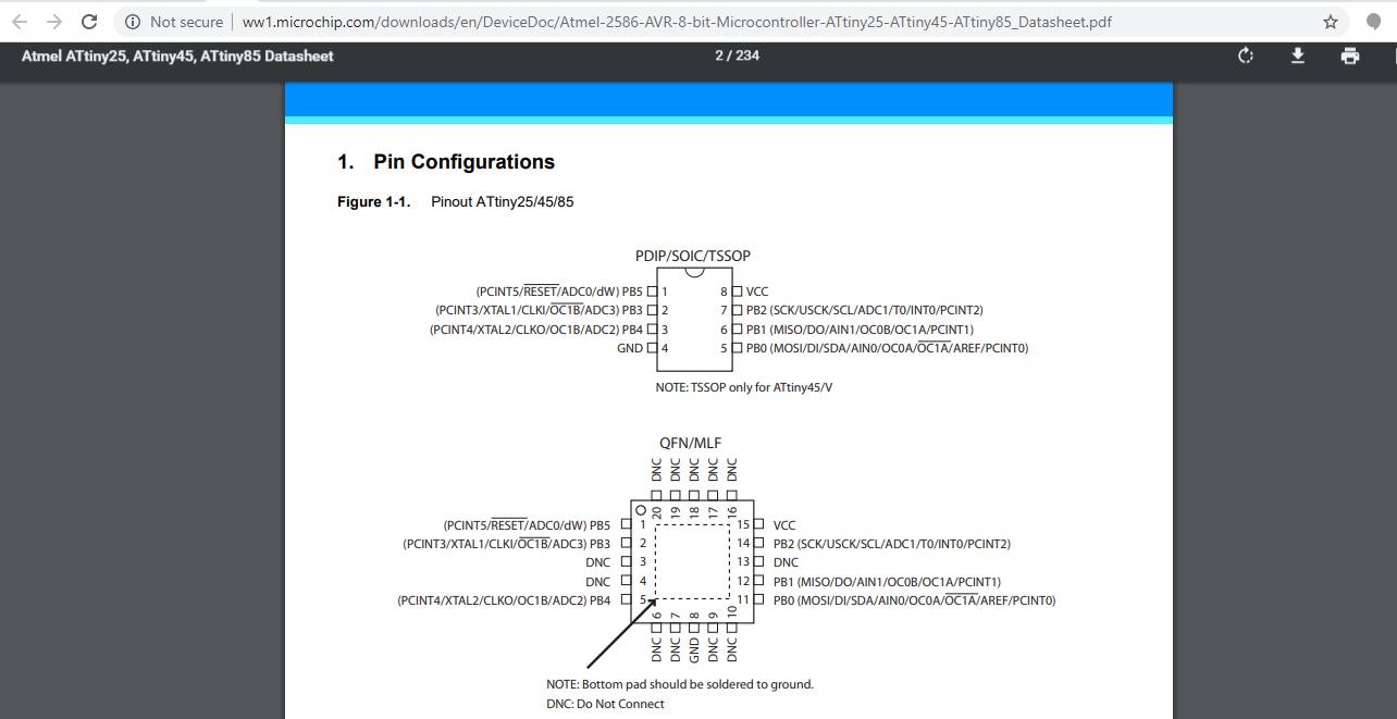
Pin Descriptions
1. VCC
Supply voltage.2. GND
Ground.3. Port B (PB5:PB0)
Port B is a 6-bit bi-directional I/O port with internal pull-up resistors (selected for each bit). The Port B output buffers have symmetrical drive characteristics with both high sink and source capability. As inputs, Port B pins that are externally pulled low will source current if the pull-up resistors are activated. The Port B pins are tri-stated when a reset condition becomes active, even if the clock is not running. Port B also serves the functions of various special features of the ATtiny25/45/85 as listed in “Alternate Functions of Port B” on page 60.
On ATtiny25, the programmable I/O ports PB3 and PB4 (pins 2 and 3) are exchanged in ATtiny15 Compatibility Mode for supporting the backward compatibility with ATtiny15.
4. RESET
Reset input. A low level on this pin for longer than the minimum pulse length will generate a reset, even if the clock is not running and provided the reset pin has not been disabled. The minimum pulse length is given in Table 21-4 on page 165. Shorter pulses are not guaranteed to generate a reset.
The reset pin can also be used as a (weak) I/O pin.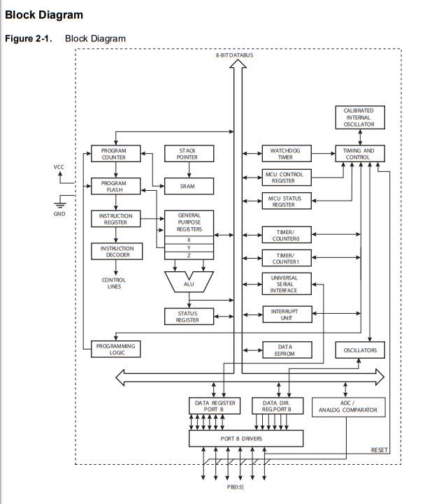
This is the architectural view.The main function of the CPU core is to ensure correct program execution. The CPU must therefore be able to access memories, perform calculations, control peripherals, and handle interrupts.In order to maximize performance and parallelism, the AVR uses a Harvard architecture – with separate memories and buses for program and data.
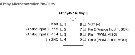
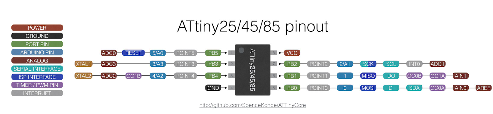
This is the Pin Diagram of ATtiny 45 microcontroller.It has two PWM pin and three analog input pin.
Programming the ISP Board
I followed this tutorial for programming Attiny45 through Arduino:
Set Up
First I downloaded the Arduino IDE for Windows. This is how the software looks like.
I had very little experience using Arduino, so I'm not familiar with the interface and coding using the Arduino functions. To use my FabISP as a programmer and my Board as a programmable board, I followed this tutorial from the High-Low Tech at MIT MediaLab.
I'll show you the steps for what I did.
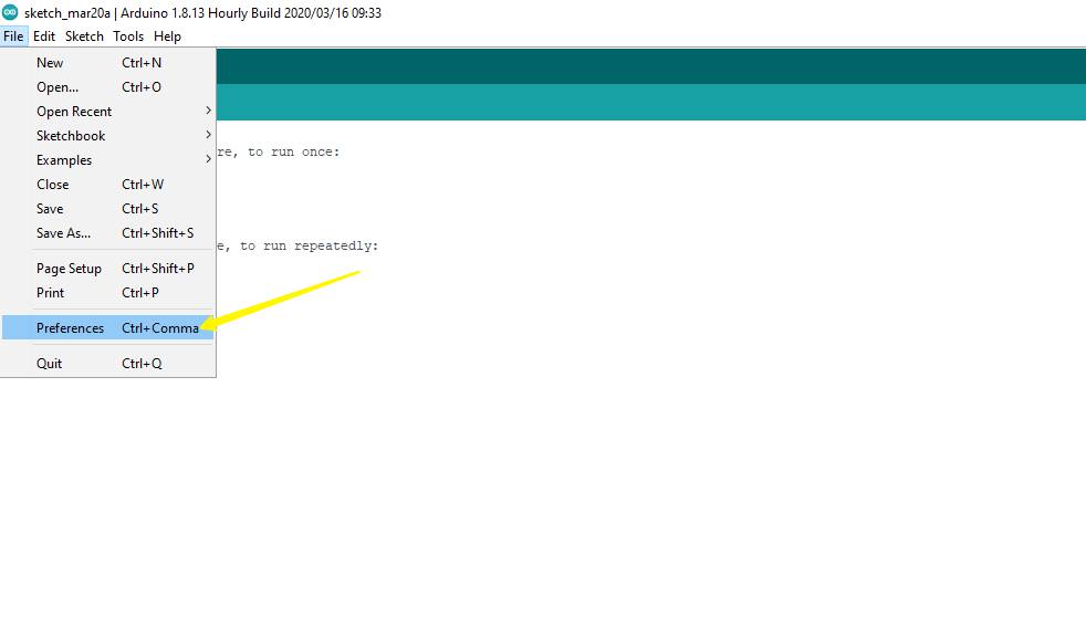
- Go to File > Preferences
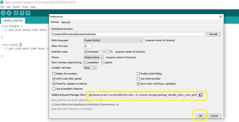
- On the Preferences windows, on the Additional Boards Manager URLs section, paste the followed link (Note: if you have already a URL like I did, just write a "," at the end of the previous one and then paste the new one):
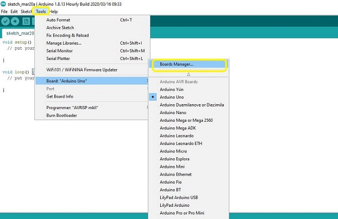
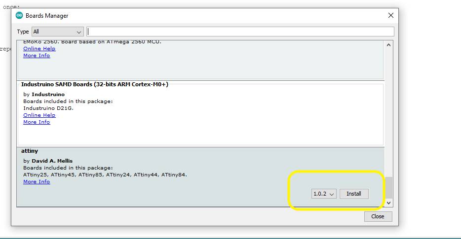
- Go to Tools > Board > Boards Manager...
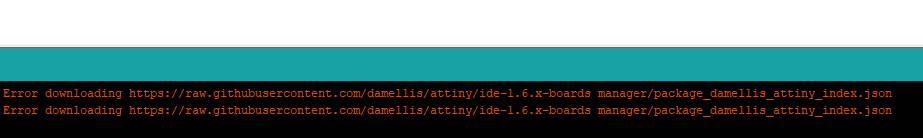
- Initially i got this error and in second attempt,downloded the library.
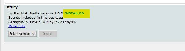
- On the Boards Manager window, look for the "attiny" by David A. Mellis package, and click Install. Then close the window.
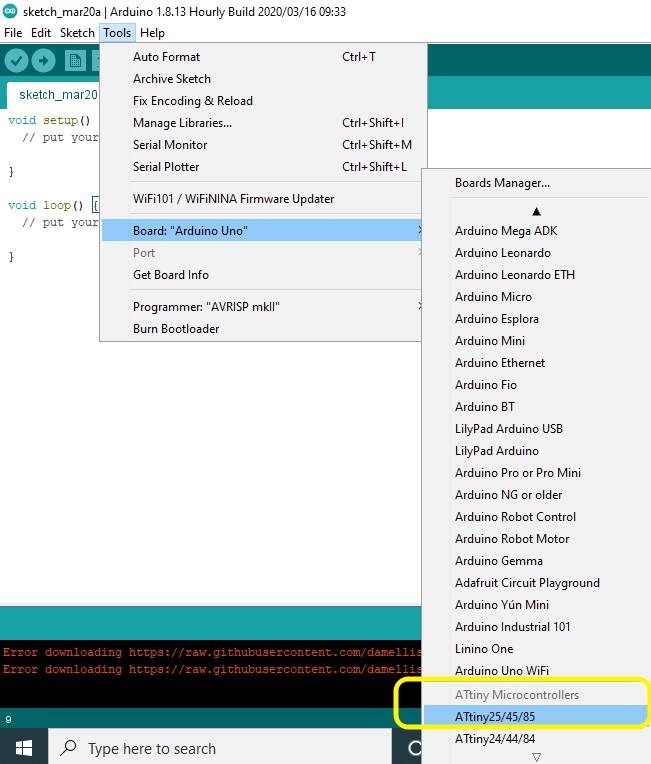
- Go again to Tools > Board, and select the ATtiny25/45/85 under the ATtiny Microcontrollers section.
https://raw.githubusercontent.com/damellis/attiny/ide-1.6.x-boards manager/package_damellis_attiny_index.json
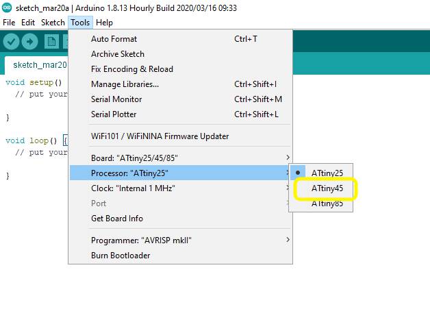
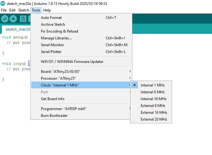
Please select 1 MHz internal memory if you didnt give resonator or crystal in your electronic design
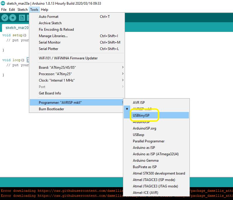
You can select USBtiny which you have developed and programmed in Electronic production week
I followed this scheme:
So, my LED is attached to Attiny´s 2 = A3, and the Button to Attiny´s 3 = A2.
So here is a programme of LED blinking on Arduino IDE for the same.
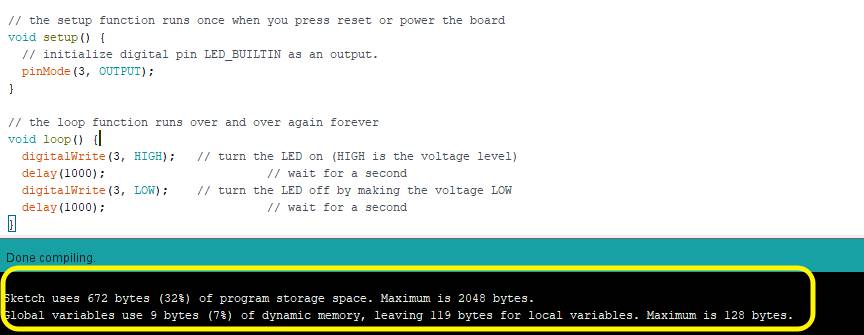
                // the setup function runs once when you press reset or power the board
                void setup() {
                  // initialize digital pin LED_BUILTIN as an output.
                  pinMode(3, OUTPUT);
                }

                // the loop function runs over and over again forever
                void loop() {
                  digitalWrite(3, HIGH);   // turn the LED on (HIGH is the voltage level)
                  delay(1000);                       // wait for a second
                  digitalWrite(3, LOW);    // turn the LED off by making the voltage LOW
                  delay(1000);                       // wait for a second
                }
Programme for LED and Button
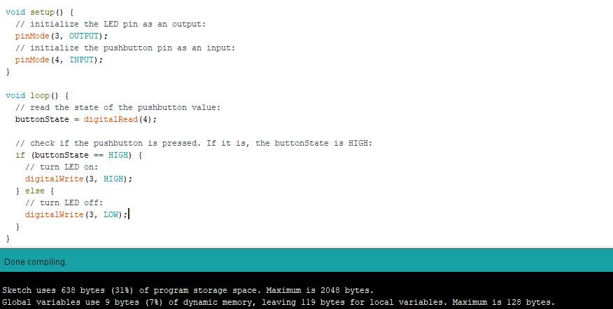
void setup() {
  // initialize the LED pin as an output:
  pinMode(3, OUTPUT);
  // initialize the pushbutton pin as an input:
  pinMode(4, INPUT);
}

void loop() {
  // read the state of the pushbutton value:
  buttonState = digitalRead(4);

  // check if the pushbutton is pressed. If it is, the buttonState is HIGH:
  if (buttonState == HIGH) {
    // turn LED on:
    digitalWrite(3, HIGH);
  } else {
    // turn LED off:
    digitalWrite(3, LOW);
  }
}
Before uploading the example,Edit it according to output and input pin you have given in your microcontoller and define it in arduino code.
Simulation on Tinker CAD
Tinker Cad
Tinkercad is a free online collection of software tools that help people all over the world think, create and make. >>>Prototype your electronic designs completely within the browser, before building them in real life.
I tried Simulation on Arduino UNO for push button Programme
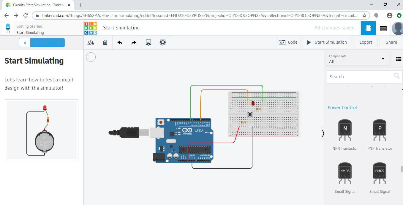
Below is the video showing simulation of same without real Board.
Work After Lockdown
Programmers :
For programmer you can use Fab USBtiny ISP,Arduino as ISP and AVRISP mkII
I have programmmed the final project baord having Attiny 44 with AVR ISP mkII and ATmega 328p using Arduino as ISP as well as with AVR ISP mkII.
This is the tutorial you can use to program Atttiny 44 with arduino as ISP.
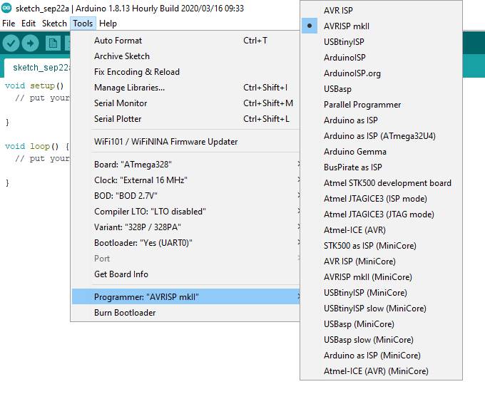
The process for Arduino as ISP and AVR ISP programmer is almost similar.In case of Arduino as Isp you need to connect these pins : Arduino Pin 13 ---> SCK Arduino Pin 12 ---> MISO Arduino Pin 11 ---> MOSI Arduino Pin 10 ---> RESET Arduino 5V ---> VCC Arduino Ground ---> GND First select "Arduino as ISP" under Tools > Programmer. Select ATtiny from Tools > Board. Select the specific ATtiny you are using (44/45/84/85) from Tools > Processor. Next select "8 MHz (Internal)" from Tools > Clock. It is important that you select Internal. Do NOT select "external" as your ATtiny will not work unless you attach an external clock to it (The ATtiny will keep these settings until you explicitly change them). Finally, select "Burn Bootloader" under tools and wait for it to complete.
AVR ISP Programmer
The process above was explained to program attiny and I selected 45 from attiny package but I dint use Attiny 45 after lockdown when in actual I followed this procedure to program my this board .
Bootloader
It is a special piece of code that is executed at every reset of the microcontroller and that looks for a sketch to be uploaded from the serial/USB port using a specific protocol and speed. If no connection is detected, the execution is passed to the code of your sketch.This little (usually 512 bytes) piece of code is called the “Bootloader” and it is in an area of the memory of the microcontroller – at the end of the address space - that can’t be reprogrammed as a regular sketch and had been designed for such purpose.
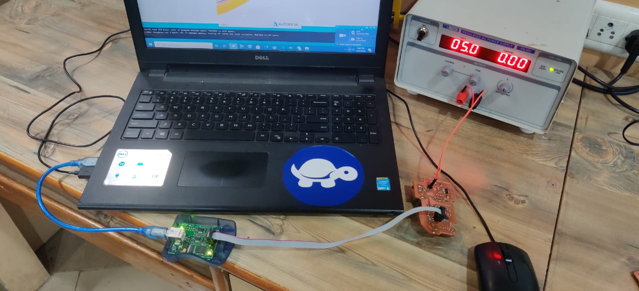
We need to burn bootloader first in order to program microcontroller with external programmer later.I used AVRISP MKII as external programmer
By default Attiny uses 1 Mhz internal, To change fuse settings from 1 Mhz to 8 Mhz you have to burn bootloader selecting 8 Mhz internal as clock and to change fuse to any other setting of cock such as external.You need to burn bootloader to set proper fuse which contain information about clock etc to the board before you use it for that setting.
It is important to give power supply of 5V externally when you are programming microcontroller with AVR ISP mkII.
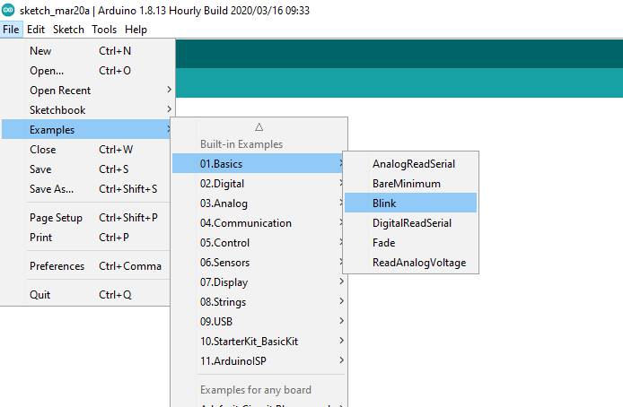
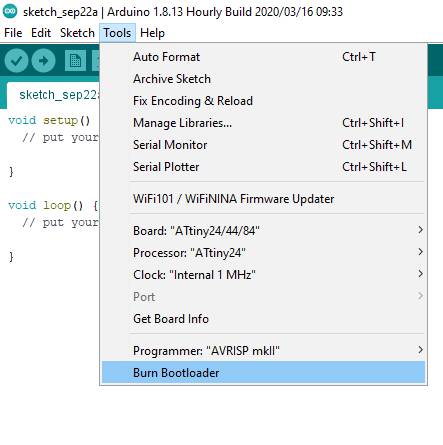
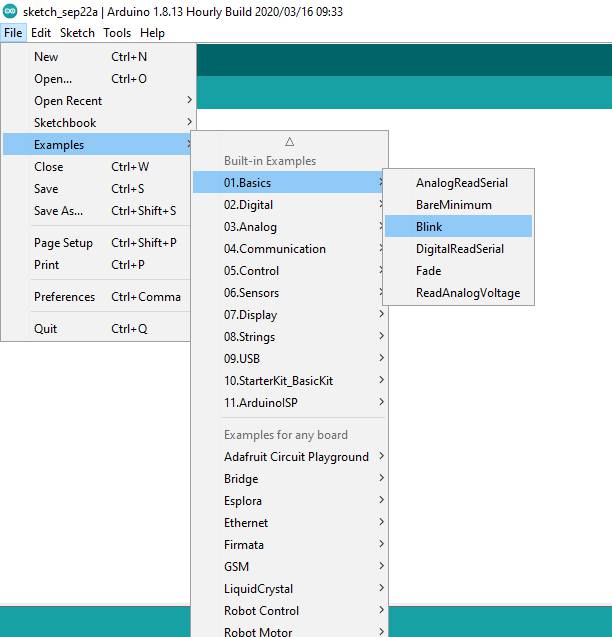
After Burning Bootloader you can used Blink code from examples by clicking on File>Examples>Basic>Blink
Burning Bootloader in ATtiny 44
This is the way I burnt bootloader in my pre final board.
Uploading Blink Code in ATtiny 44
In this video you can see I upload program using programmer
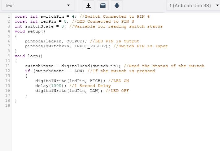
Blink Code
Here after uploading, The LED is blinking with power supply 5V
How to program ATmega 328p with AVR ISP
Here you can read the datasheet of ATmega 328p.
Board manager Url, Paste the link below to install ATmega 328p in Boards Manager
"https://mcudude.github.io/MiniCore/package_MCUdude_MiniCore_index.json"
Search Mini Core in Boards Manager and install it.
I got this link from this pageSelect Atmega 32P as shown in image below and Click on Burn Bootloader
The process is same as explained above Attiny 44 to program it with AVRISP mkII.
Group Assignment
Our assignment was to compare the performance and development workflows for other architectures
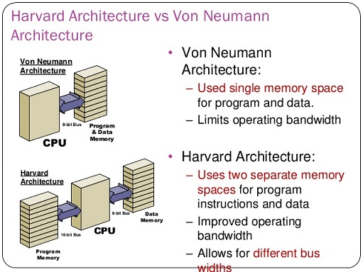
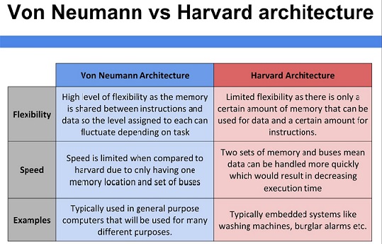
Architecture of a micro computer or a micro controller refers to the a>rrangement of the CPU with respect of the RAM and ROM. Hence, the Von-Neuman and Harvard architecture are the two ways through which the micro controller can have its arrangement of the CPU with RAM and ROM.
Computer Architecture refers to the internal design of a computer with its CPU, which includes:- • Arithmetic and logic unit
- • Control unit
- • Registers
- • Memory for data and instructions
- • Input/output interface
- • External storage functions
The same memory and bus are used to store both Data and Instructions
The main drawback:- CPU is unable to access program memory and data memory simultaneously.
- This case is called the "bottleneck" that affects system performance.
- • If a Von-Neumann machine wants to perform an instruction (already fetched from the memory) on some data in memory, it has to move the data across the bus into the CPU.
- • When the computation is done, it needs to move outputs of the computation to memory across the same bus; this operation will be completed if the bus is not used by another operation to fetch another instruction or data from the shared memory; otherwise the outputs of the computation has to wait.
Applications and features of Von Neumann Architecture
The Von Neuman architecture has got extensive application in everyday life. Keeping in mind the extensive application the Von Neuman architecture has been introduced as a subject in the engendering degree. From the third semester engineering students will have the subject as their curriculum. The Von Neuman architecture consists of some important features and here we will have a detailed elaboration to the features.
Harvard architecture:The Harvard architecture stores machine instructions and data in separate memory units using different buses.
The main advantage:Computers designed with the Harvard architecture are able to run a program and access data independently, and therefore simultaneously.
Harvard architecture is more complicated but separate pipelines remove the bottleneck that Von-Neumann creates.
Applications and features of Harvard Architectures
The principal advantage of the pure Harvard architecture—simultaneous access to more than one memory system—has been reduced by modified Harvard processors using modern CPU cache systems. Relatively pure Harvard architecture machines are used mostly in applications where trade-offs, like the cost and power savings from omitting caches, outweigh the programming penalties from featuring distinct code and data address spaces. Digital signal processors (DSPs) generally execute small, highly optimized audio or video processing algorithms. They avoid caches because their behavior must be extremely reproducible. The difficulties of coping with multiple address spaces are of secondary concern to speed of execution. Consequently, some DSPs feature multiple data memories in distinct address spaces to facilitate SIMD and VLIW processing. Texas Instruments TMS320 C55x processors, for one example, feature multiple parallel data buses (two write, three read) and one instruction bus. Microcontrollers are characterized by having small amounts of program (flash memory) and data (SRAM) memory, and take advantage of the Harvard architecture to speed processing by concurrent instruction and data access. The separate storage means the program and data memories may feature different bit widths, for example using 16-bit wide instructions and 8-bit wide data. They also mean that instruction prefetch can be performed in parallel with other activities. Examples include the PIC by Microchip Technology, Inc. and the AVR by Atmel Corp (now part of Microchip Technology). The speed aspect : A lot has been discussed about the Harvard architecture, but without the speed any architecture can’t be accepted. But in case of the Havard architecture the manufacturers have designed the architecture in such a way that it will be able to process the data with a much higher speed. Yes, all care has been taken so that the architecture can process data with a high speed. By implementing the same formula the modern days CPU are being manufactured so that the new CPU can run with a much faster sped and can also process the data effectively. The concept of the CPU cache is also being implemented while designing the Harvard architecture.

