Electronics Production
In this Week I have to make a PCB or In-circuit programmer through milling Machine by using copper clad as stock,there is another process of ecthing in which chemical is used for PCB manufaturing,
and another task is to characterize the milling Machine as a group assignment which we have in our Fablab ie SRM 2O Roland
The Roland SRM-20 MonoFab Desktop Subtractive Rapid Prototyping (SRP) system is capable of 3D milling, 2D Milling, and Engraving. The SRM-20 is ideal for a variety of product designs tasks, including model making, rapid prototyping, and small lot production.SRM-20 is transformed into a PC Board Prototype System, an Engraver, a Jewelry Wax Carving system.
As my background is Mechanical,I dont know much about PCB,so first
come to What is In-circuit Programmer?
In-system programming (ISP), also called in-circuit serial programming (ICSP), is the ability of some programmable logic devices, microcontrollers, and other embedded devices to be programmed while installed in a complete system, rather than requiring the chip to be programmed prior to installing it into the system.
It allows firmware updates to be delivered to the on-chip memory of microcontrollers and related processors without requiring specialist programming circuitry on the circuit board, and simplifies design work.
Due to supply management issues we was unable to start work with SRM 20 for first few days,
So we go with the idea that we will start working on Vinyl plotter with Copper tape which was available.But the idea got failed
as we don't have that base which is required to hold the Copper tape.
Steps are as following:
STEP 1
>First I dowloaded the Hello.isp file from here ISP
STEP 2
Then I used Graphtec Studio for cutting the png file on vinyl Ploter,I Cut it at the setting shown:
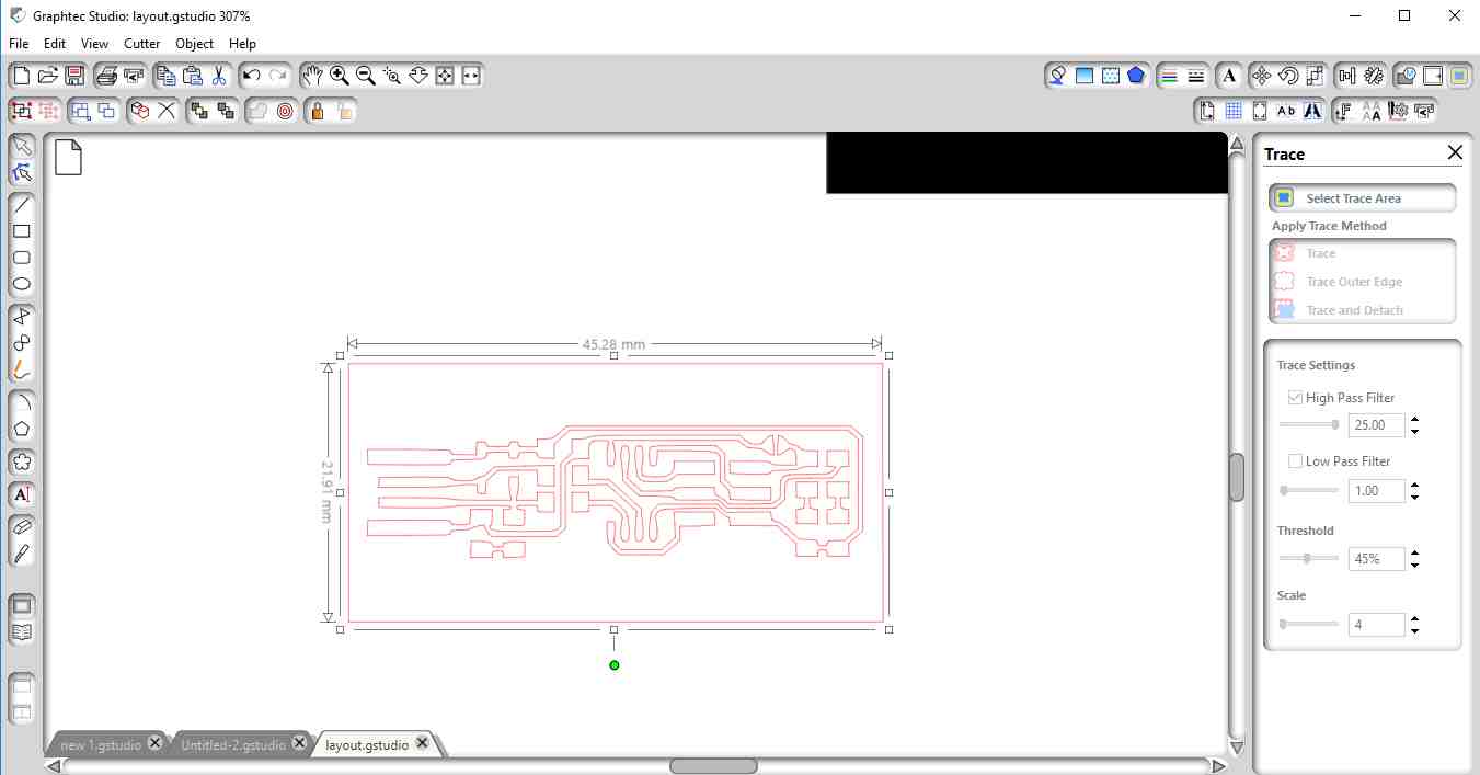
This image is showing the trace of ISP on acrylic sheet with vinyl sheet.
STEP 3
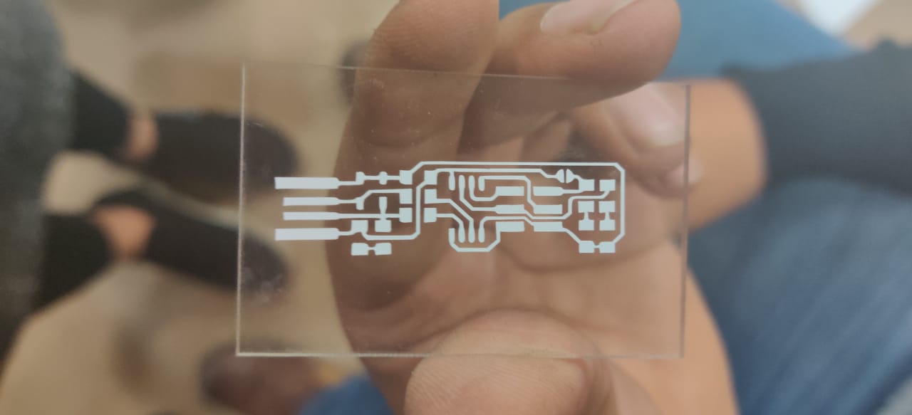
Then we did various steps on sticking Copper tape on Vinyl Sheet as well as on Sacrificial sheet shown: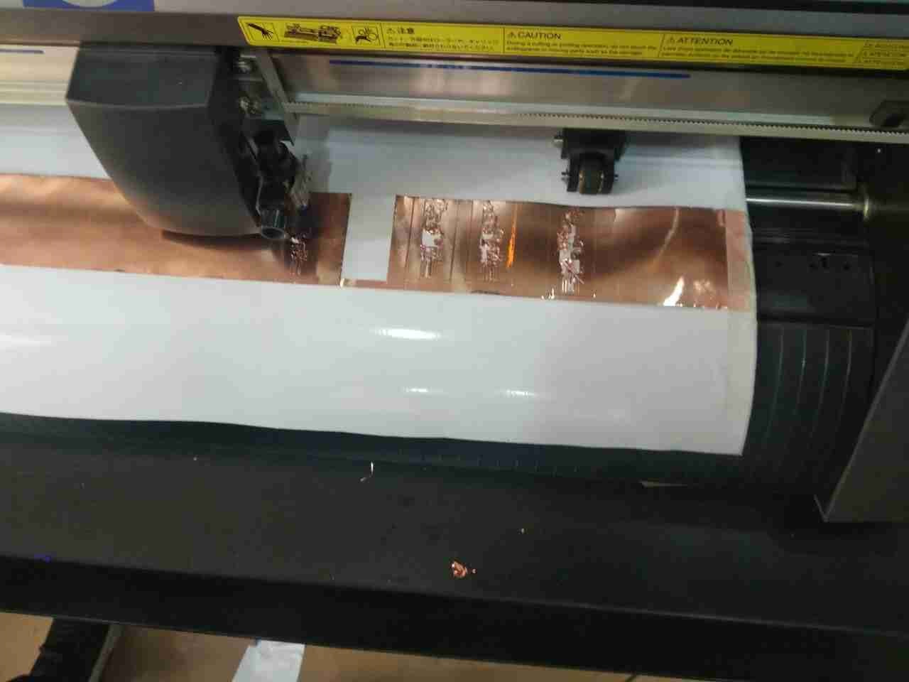
For this Force setting were 7,8,9 and speed was 3cm/sec.Also got one on sheet but due to weeding it didnt come out properly.
Group Assignment
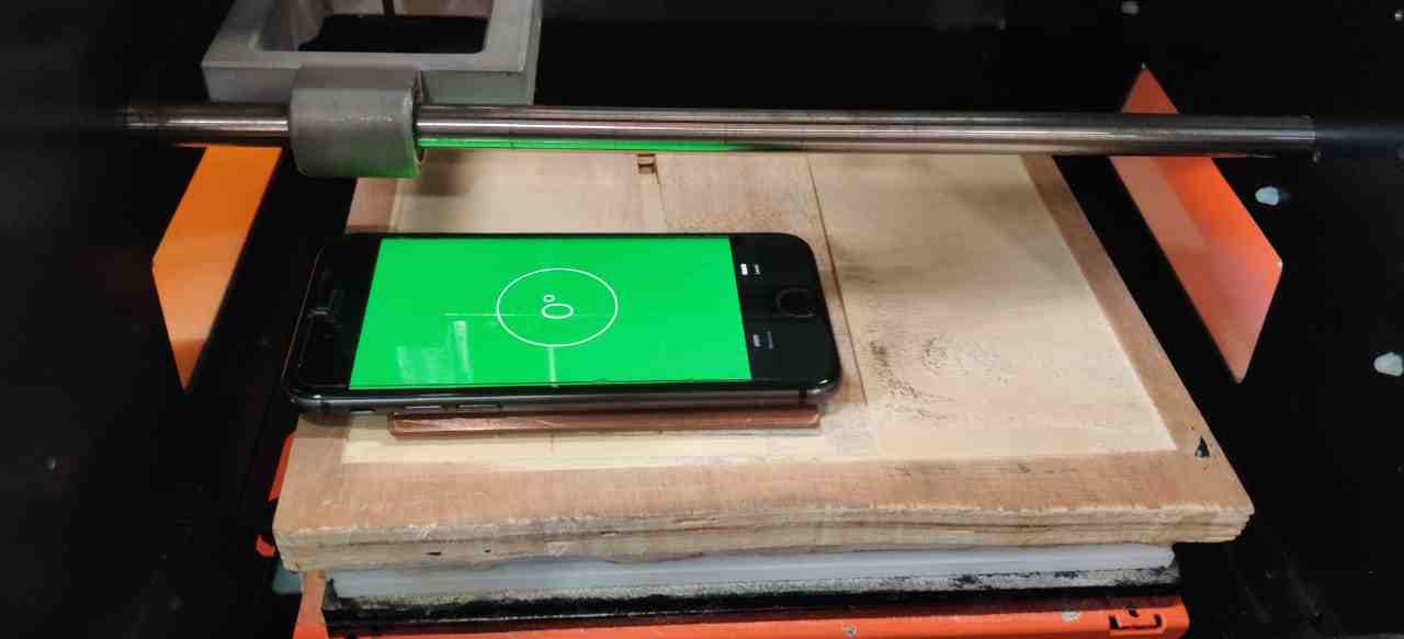
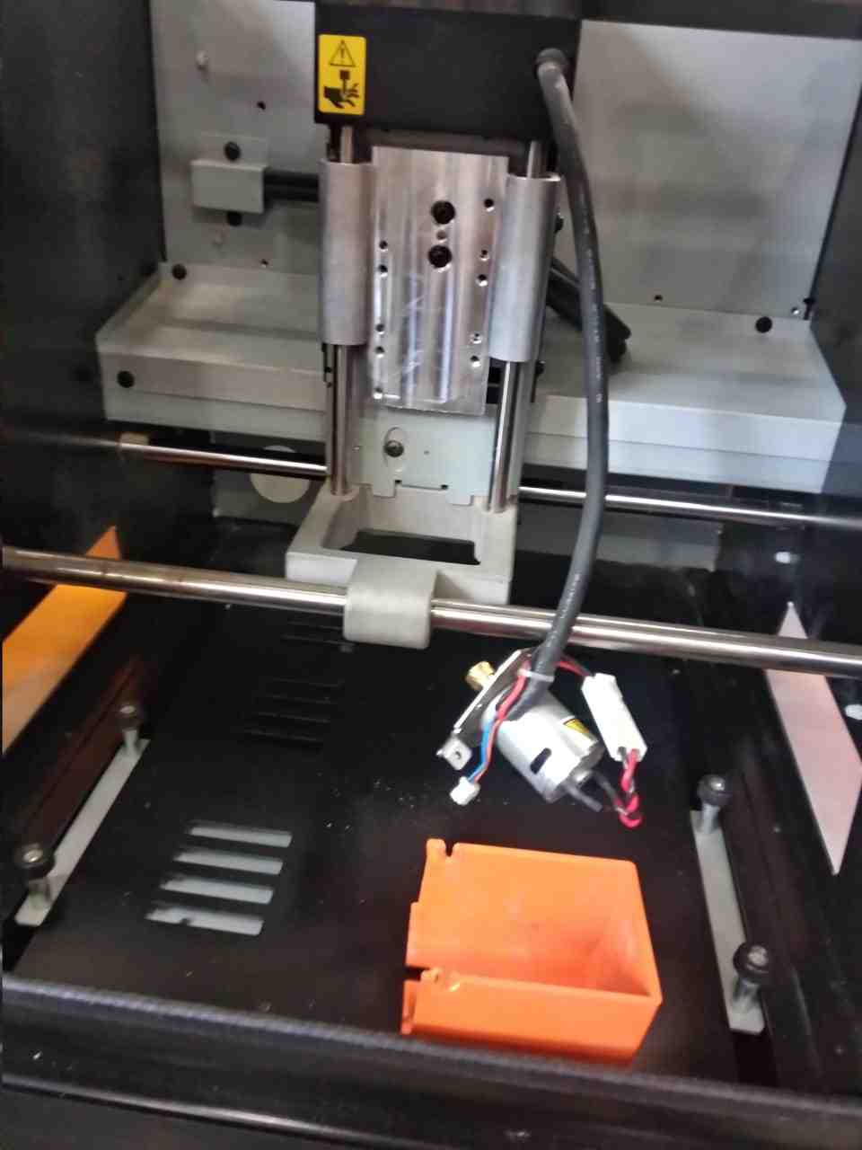
As SRM 20 was not in good condition it need to be service properly,So our local instructor Rahul first clean the SRM 20 with Vacuum Cleaner. The Bed was of wood and the levelling was not okay,we do the leveling test with help of inbuilt feature of I-phone of our Instructor. As the tool bits was not available in lab,the process of dispatching was in process.
For time being we make the PCB, with the help of V tool bit.
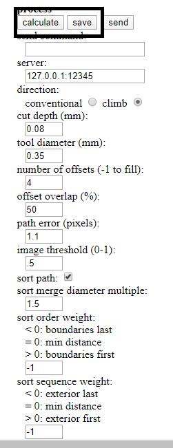
First we got to know about V-panel which is the software that was installed in the desktop already.The first thing we learnt is that how to do the Zeriong ie to set the tool of SRM at home position.(x=0,Y=0,Z=0) manually. we did test cut on one of the PCB availabe on Neils Board as to check the traces of ISP. Below is the interface showing V-panel
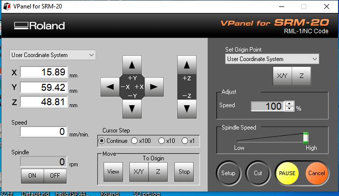
The SRM-20’s VPanel controller provides a simple interface for adjusting tool position and moving the cursor to set the milling starting point. The VPanel also allows easy control of feed rate and spindle speed with pause and resume operation, plus tracking of X,Y,Z axis milling with a numeric readout in millimetres or inches.
Source : https://www.rolanddg.co.in/products/3d/srm-20-small-milling-machine/features
The traces of PCB was not clear and appropriate as there was tool wear and bed was not levelled.
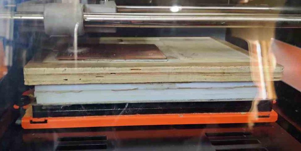
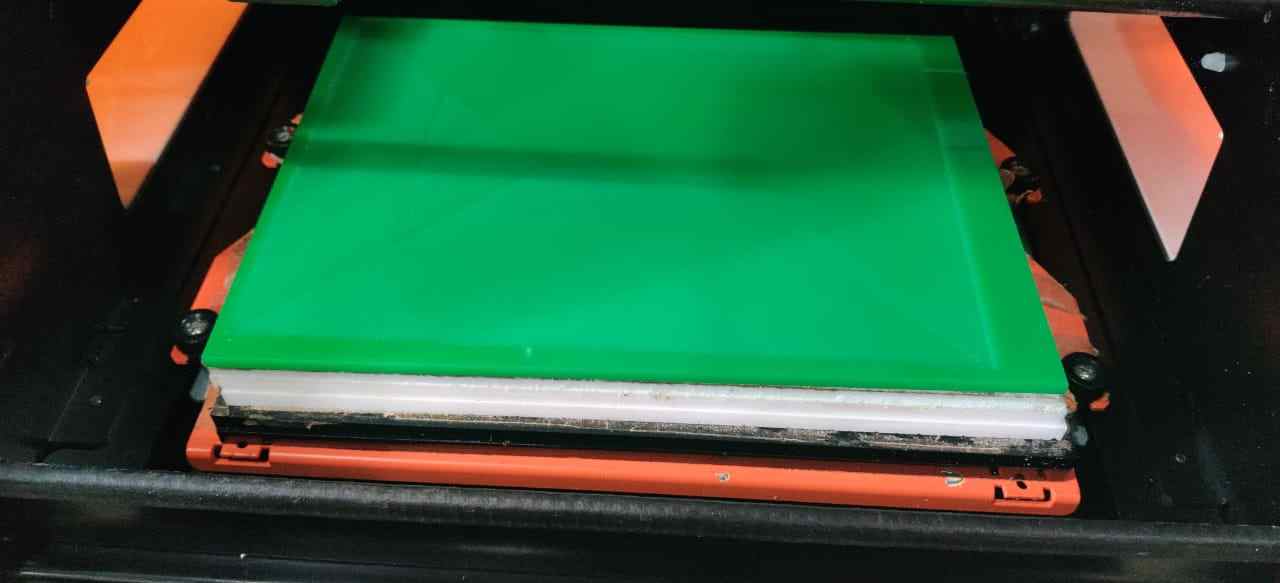
So we decided to change the bed material from wood to acrylic then with the help of Laser cuttting machine,I cut down the Bed Size Acrylic sheet of 150*210mm
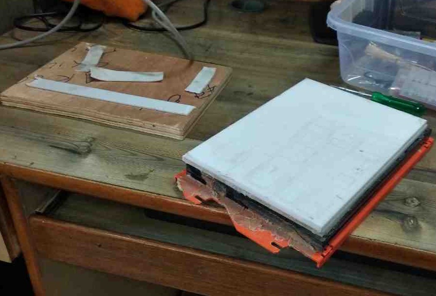
The acrylic sheet color was green and then surfacing of Bed was done by our instructor. It took lot of time.We used Click Mill for this process.
Also the machine oil has been poured in bearing of head of SRM 20.
The bed was set properly with Three acrylic sheets of 5mm that was stick together to form a stiff bed.
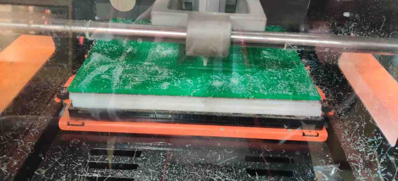
After cleaning with vacuum cleaner Now it is ready to use for group assignment test.
Installation of Software to operate SRM 20
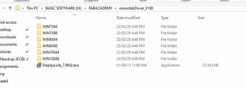
Installation of V-panel:1. As the software of SRM Roland are availabe in zip file on this link with name of Roland Onsupport Setup.
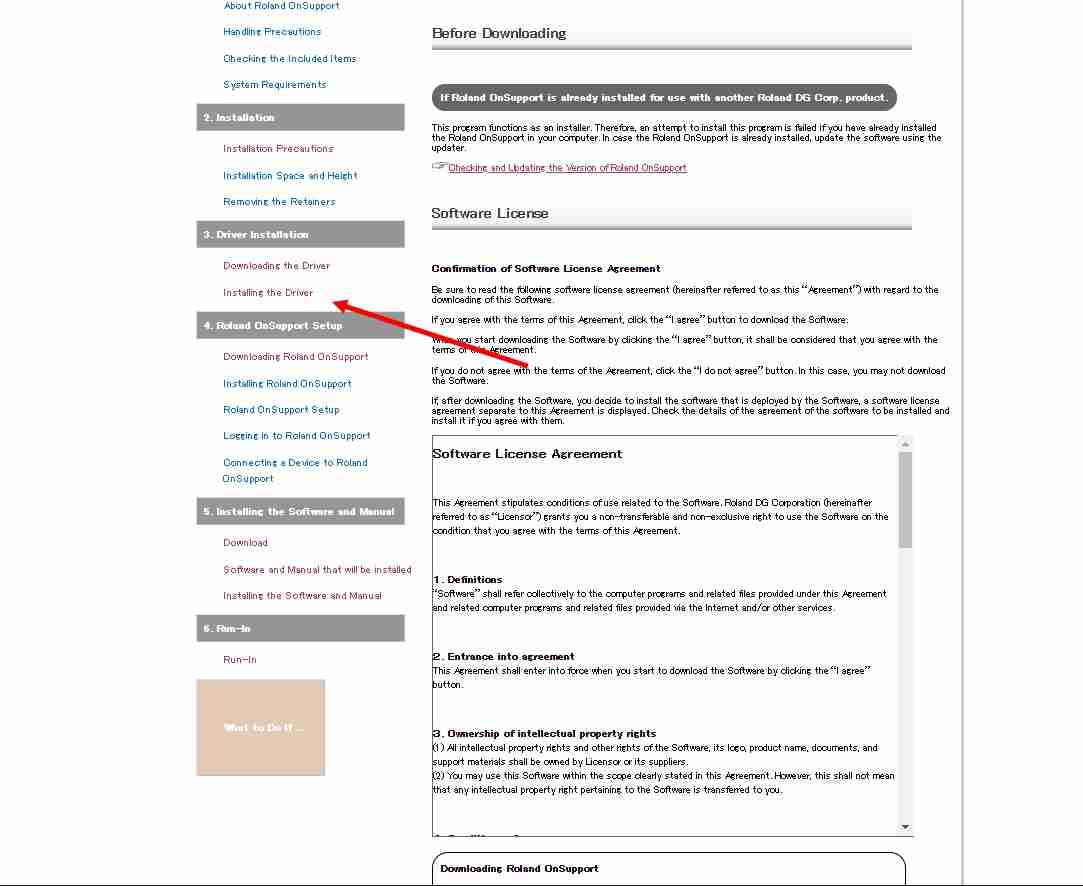
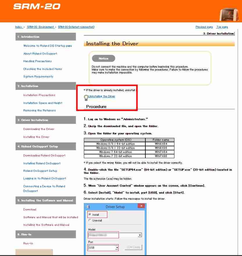
.exe file.
TEST
FIRST TEST
For the first test we tried line test for following settings:
I tried these settings on fab module.
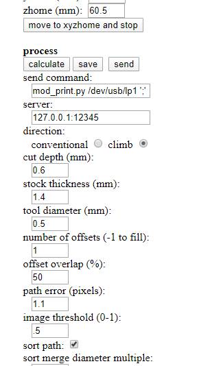
>Tool used=1/32" and 1/64"Traces Tool Setting taken on Fabmodules
>Tool Dia=0.4 mm>Depth of Cut=0.8mm
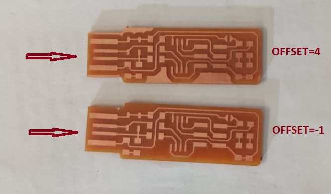
>Offet = -1
>Stock =1.4mm
>Offset Overlap=50%
>For trace we used 1/64" end mill
Cutout Tool Setting taken on Fabmodules
>Tool Dia=0.8mm>offset=1
>Depth of cut=1.4mm
>Tool used=1/32" end mill
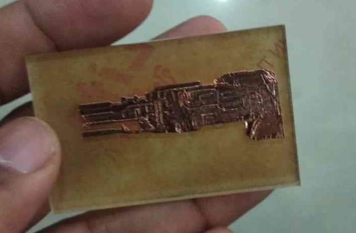
Initially We took 0.8mm depth of cut, it went too deep into the copper clad board and width of copper was less as compared to the depth of cut.
In these settings all the copper has been removed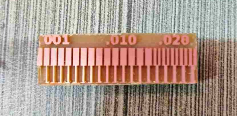
SECOND TEST
For the second test we tried line test for following settings:
-
>Tool used=V-Bit
Traces Tool Setting taken on Fabmodules
>Tool Dia=0.5 mm>Depth of Cut=0.12mm
>Offet = 4
>Stock =1.4mm
>Offset Overlap=50%
>For trace we used v-bit
Cutout Tool Setting
>For cutout tool used 1/32">offset=1
>Depth of cut=1.4mm
>Tool Dia=0.79mm
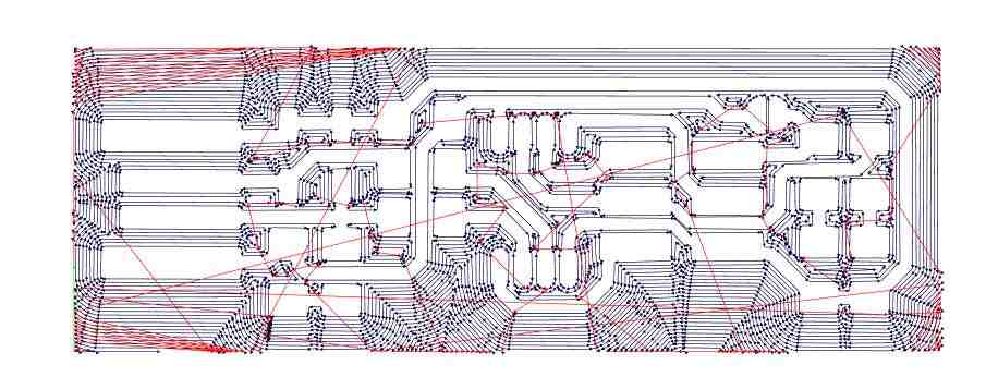
As it is V-BIT we used tool dia 0.5mm on fabmodules.In this case some some lines of copper of micron level left on board.
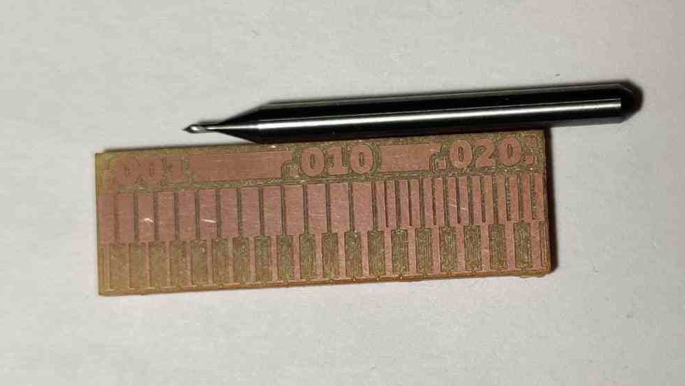
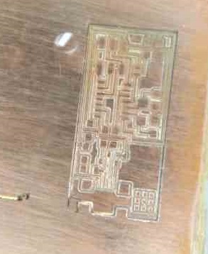
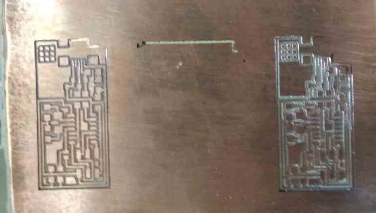
THIRD TEST
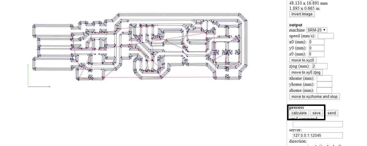
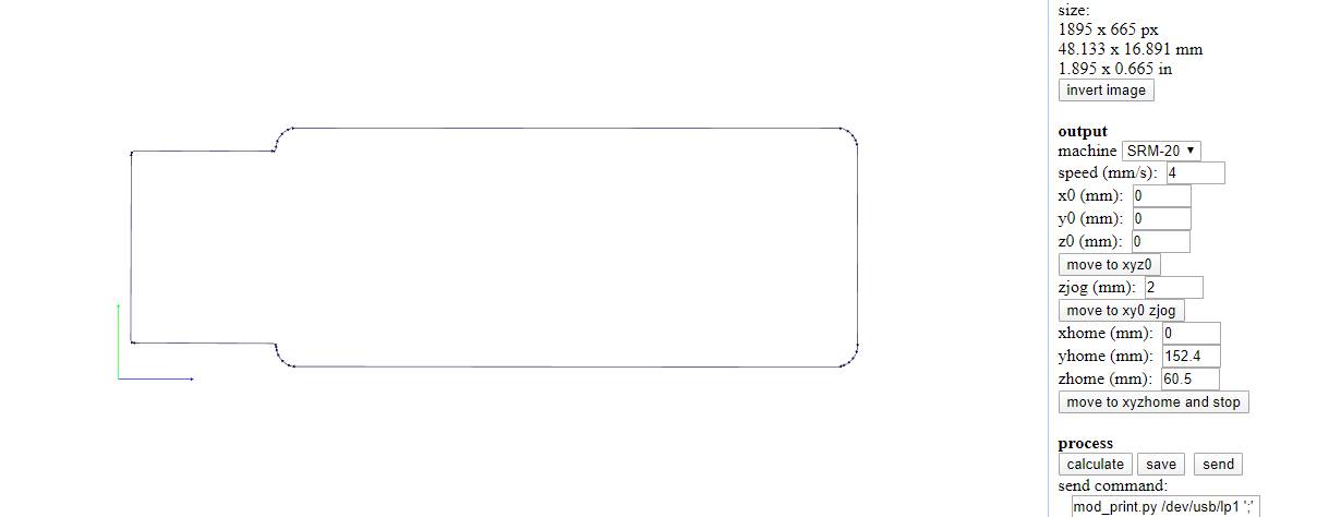
This image is showing our group assignment test which is line test for characterising of our machine. For this we have taken the settings as:
>Tool used=1/32 and 1/64Traces Tool Setting taken on Fabmodules
>Tool Dia=0.35 mm>Depth of Cut=0.1mm
>Offet = 4
>Stock =1.4mm
>Offset Overlap=50%
>For cutout we used 1/32" end mill
>For trace we used 1/64" end mill
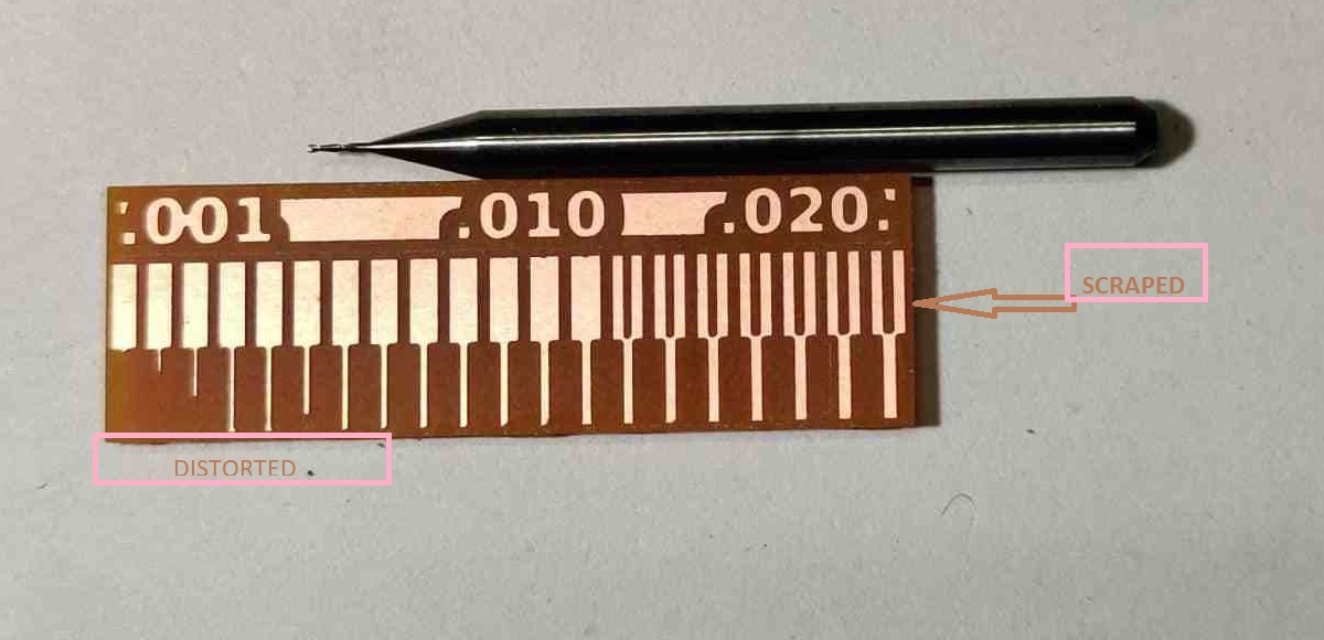
This is the result which come out proper.
For all the tests the png was downoaded from Line TestCONCLUSION
1. We find 0.1 mm depth of cut appropriate for traces.
2. The maximum clearnace come out to be 0.013 inches or 13 mil
3. The Trace width cuts upto 0.006 inches or 6 mil.
INDIVIDUAL ASSIGNMENT
Its time to mill ISP
Step 1
The first step to fabricate ISP is to download the traces and outline of ISP image form
this link
Traces
Outline cutout
Step 2 : For Trace
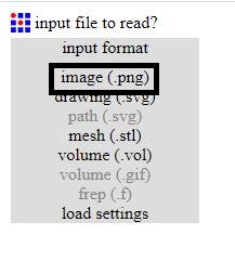
As the file which was downloaded having.PNG extension.So the help of Fabmodules
The desired format ie .RML file will be generated.
The steps are below:
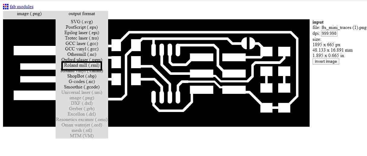
1. Select the png file in input
2. Select the output process : Roland Mill
3. Fill parameters :
- a. Depth of cut :0.08mm
- b. Offset: 4
- c. Offset Overlap: 50%
5. Save the file as .rml format
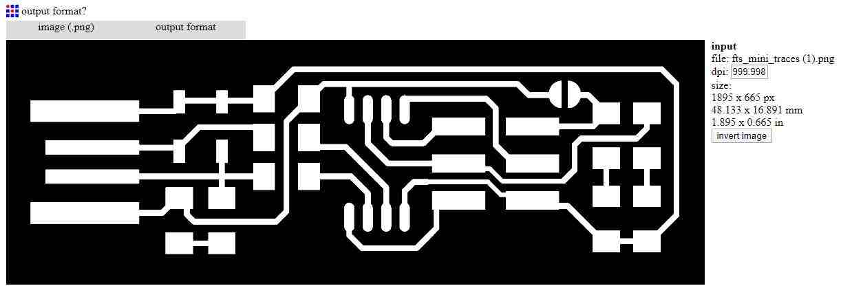
For offset: -1
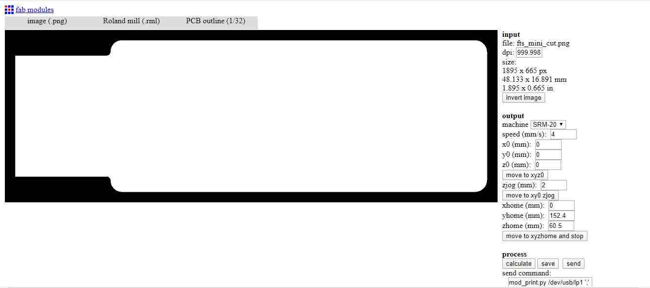
For Cutout
1. Select the png file in input
2. Select the output process:Roland Mill
3. Fill parameters
Tool Dia=0.5mm
Depth of cut :0.6mm
Offset: 1
Offset Overlap: 50%
4. Calculate the tool path
5. Save the file as .rml format
Step 3
1. The tool has been changed for the traces.2. The end mill used for traces is 1/64 inch .
3. The end mill used for cutout is 1/32 inch.
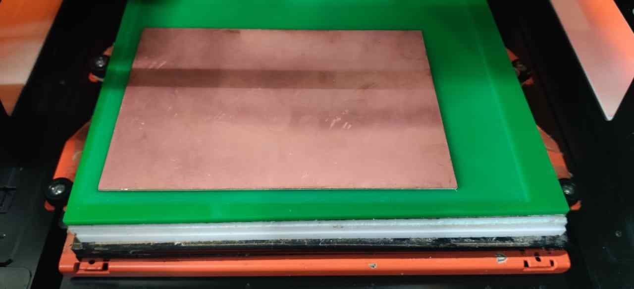
4. With thin double sided tape copper tape has been fixed to bed.
5. And with V-Panel home posittion has been set.
6. By adding file command of cut was used to start operation.
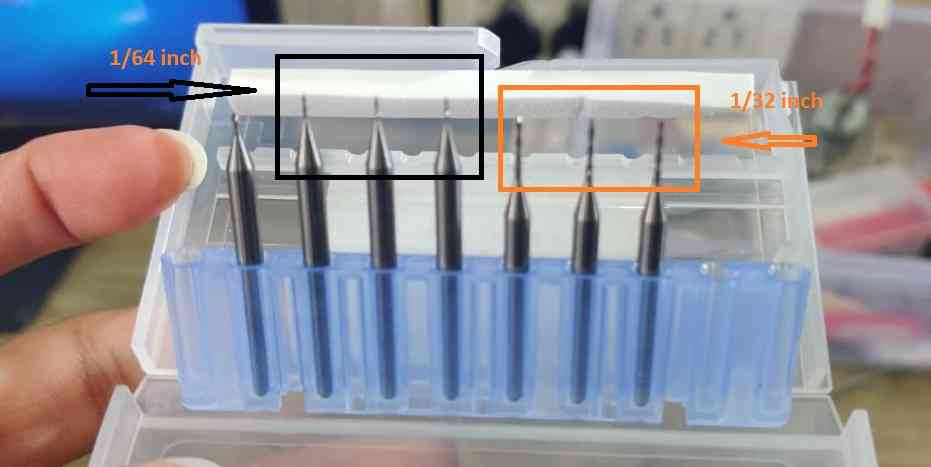
Change the required tool as for tracing-1/64" and for cutout-1/32"
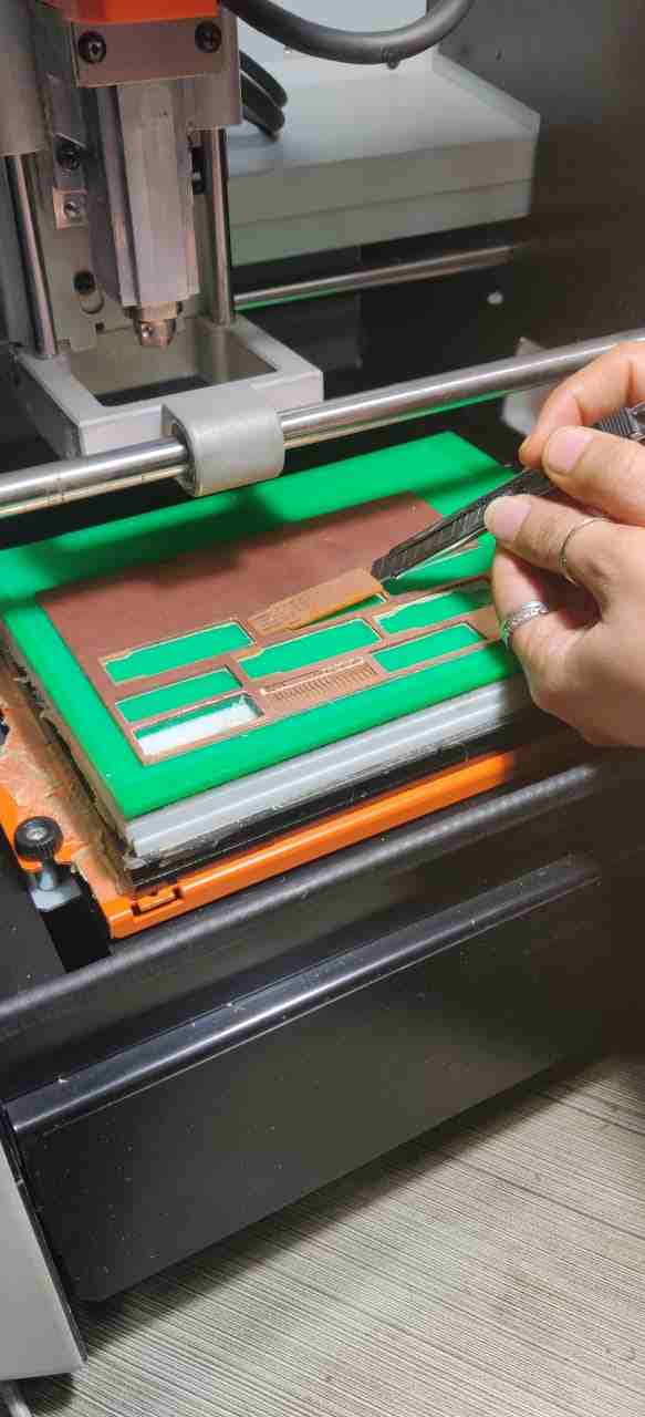
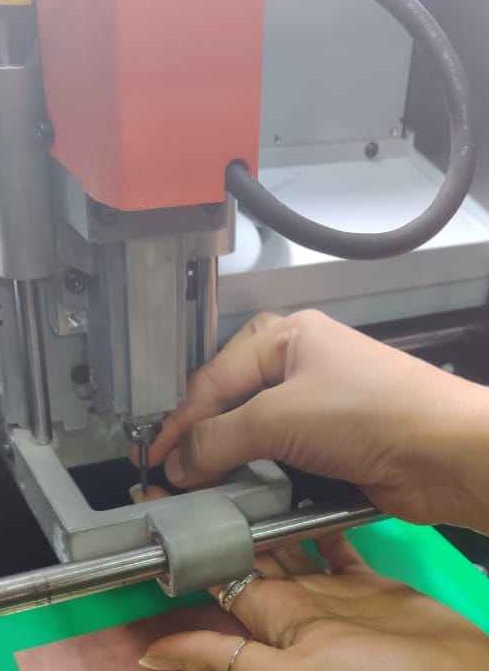
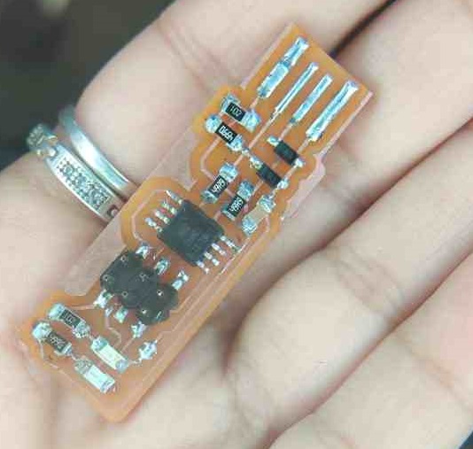
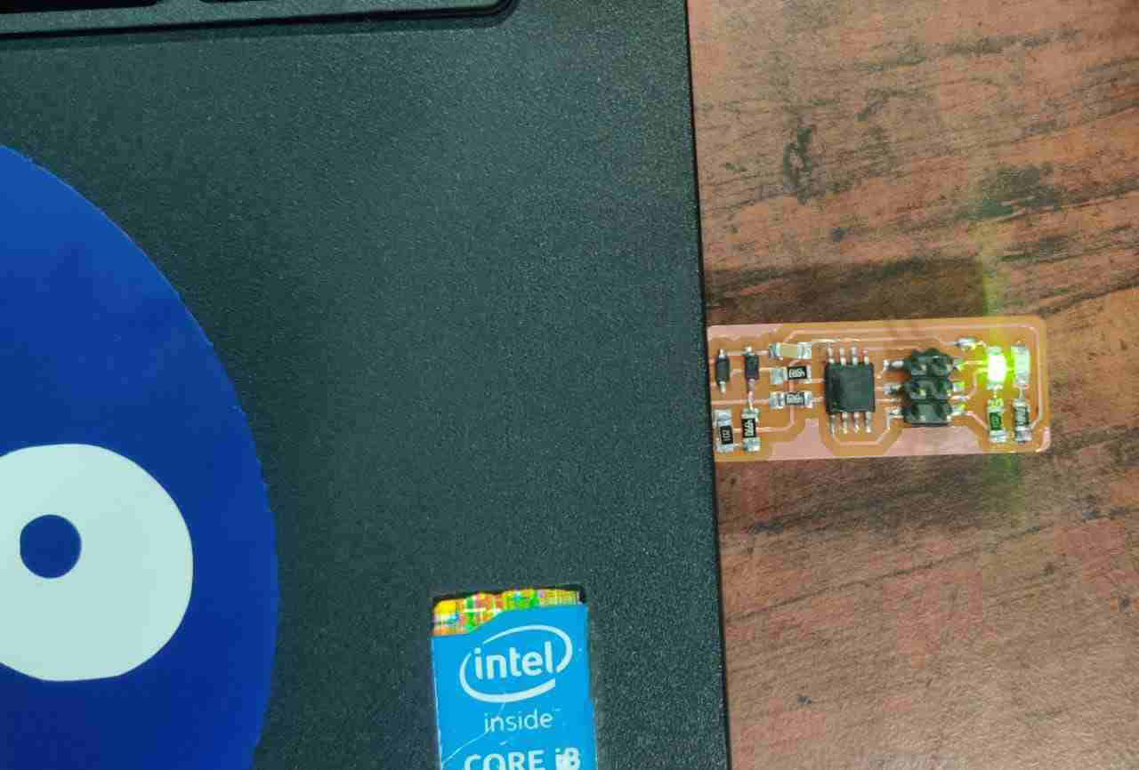
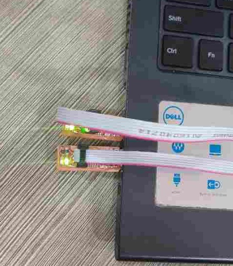
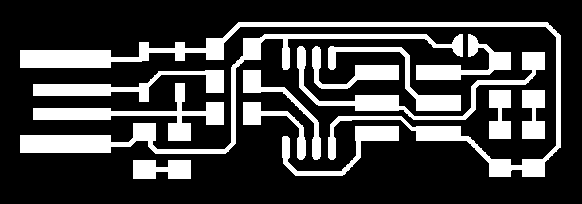
Me removing the pcb from clad baord.As from the same board, other fabmates pcb has been also cut.
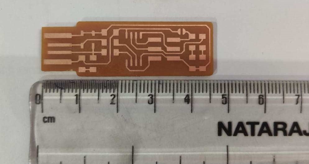
This is showing the approximately length of ISP.
Step 4
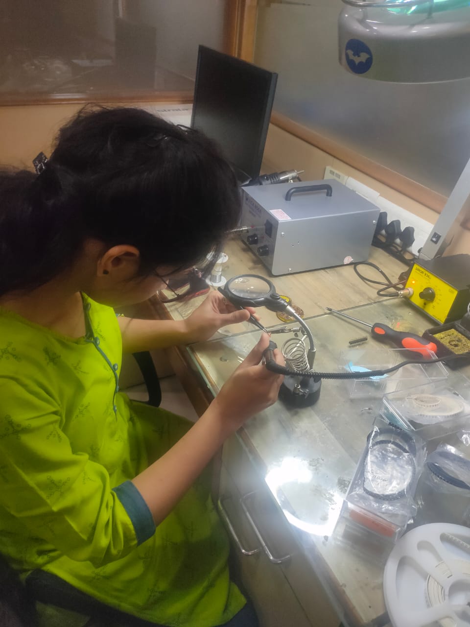
Soldering
1. List of components to be soldered on ISP.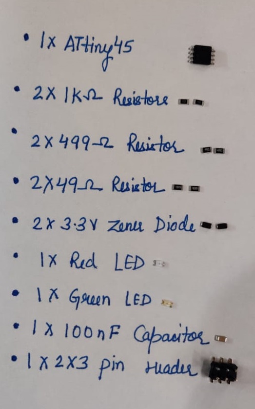
Some of these components have polarity like in 3.3 V Diode had negative polarity where there was grey light line and in case of LED(Light Emitting Diode) where there was green small spot had negative polarity and ATtiny 45 have dot First number pin was started from there. Capacitor and Reistor does not have polarity.
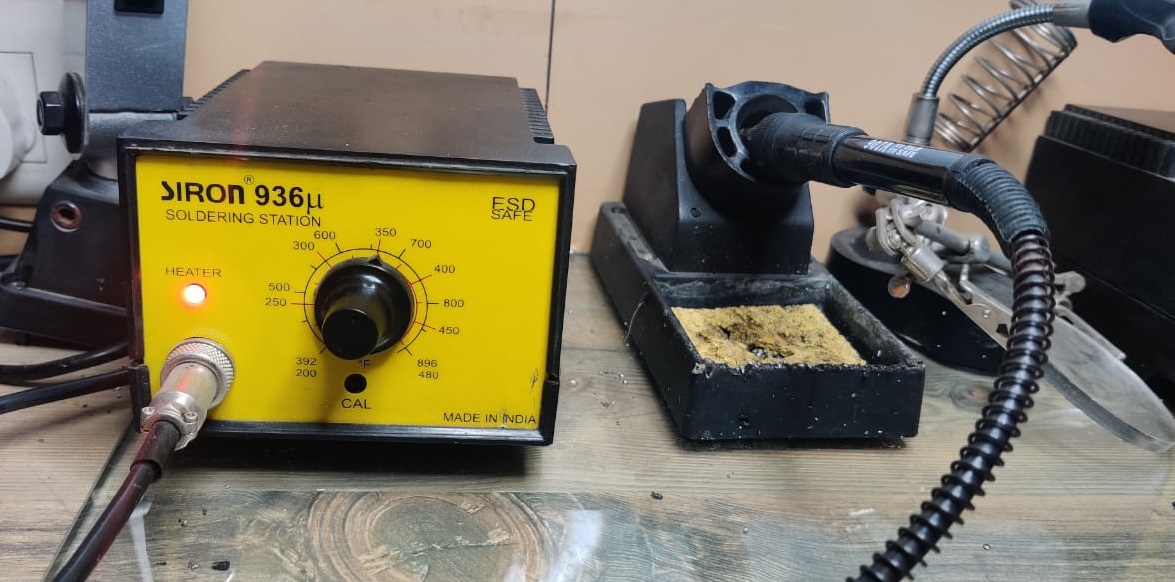
I set the parameter as 350-400 degree celcius for heating. We can vary it when we want to heat more.
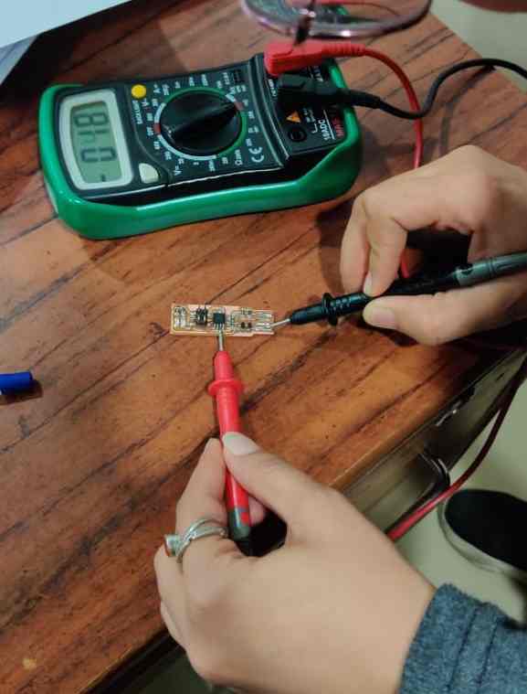
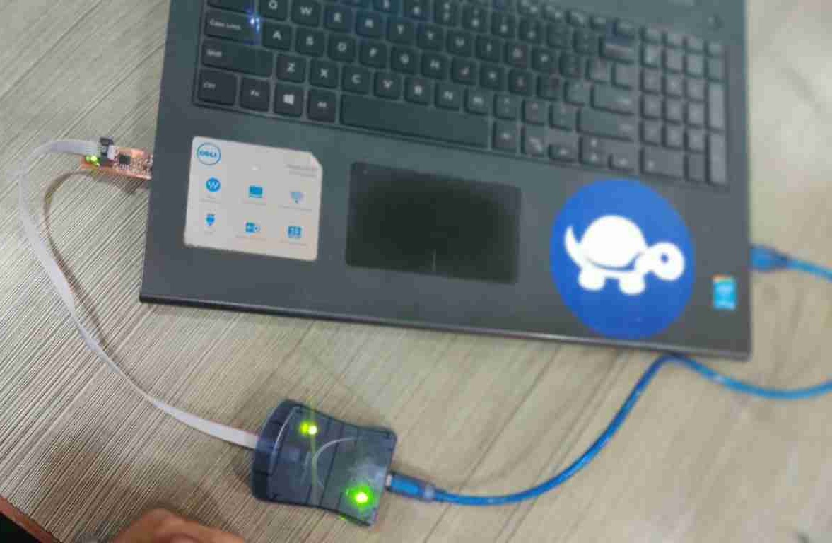
First after soldering i plugged it into my laptop and it immediately shown the green LED blinking. My instructor said it is okay Now you can go for programming.
As this is very new to me first I go with this turorial thoroughly. TUTORIAL
The software I downloaded are :1. Atmel GNU Too Chain.
2. GNU make.
3. Avrdude.
4. Zadig.
5. FTS Firmware.
I have downloaded each file/software tool and unzipped.
According to tutorial,,Then I added the paths of GNU toolchain, GNU make and Everdude by going to the control panel >> system and security >> system >> advanced system settings >> environment variable >> double click on paths >>
and add the new paths.
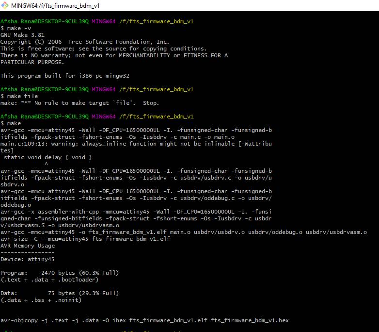
After adding the variable path setting,in command prompt I have to type
make -v and it shows the GNU politics_version.
With this step AVR Pogramme the Isp into programmer.
After that
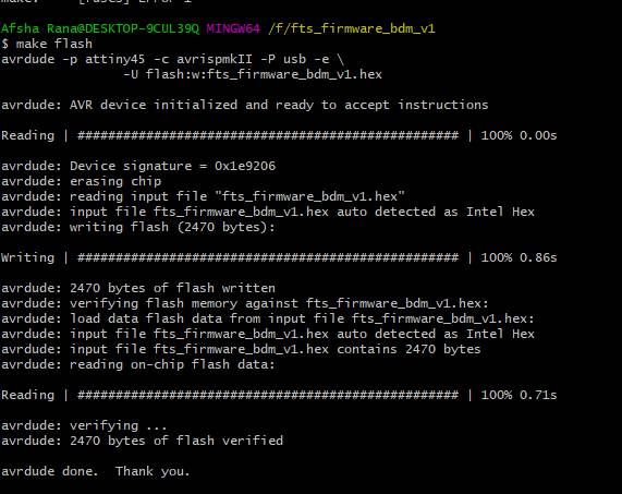
make flash is used.It generates the hex code .
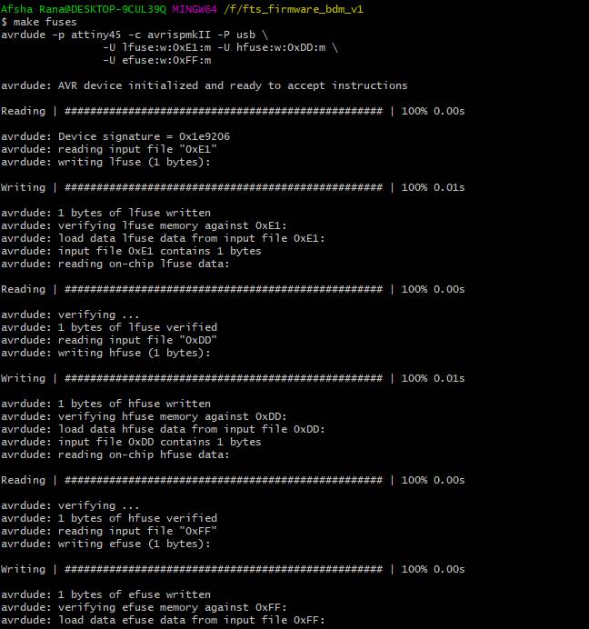
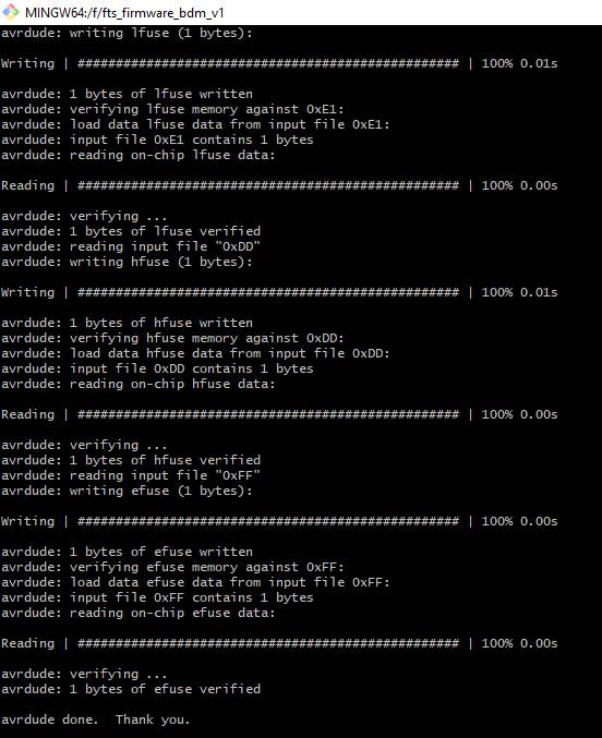
make fuses will run.
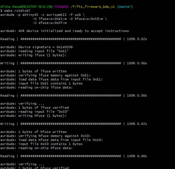
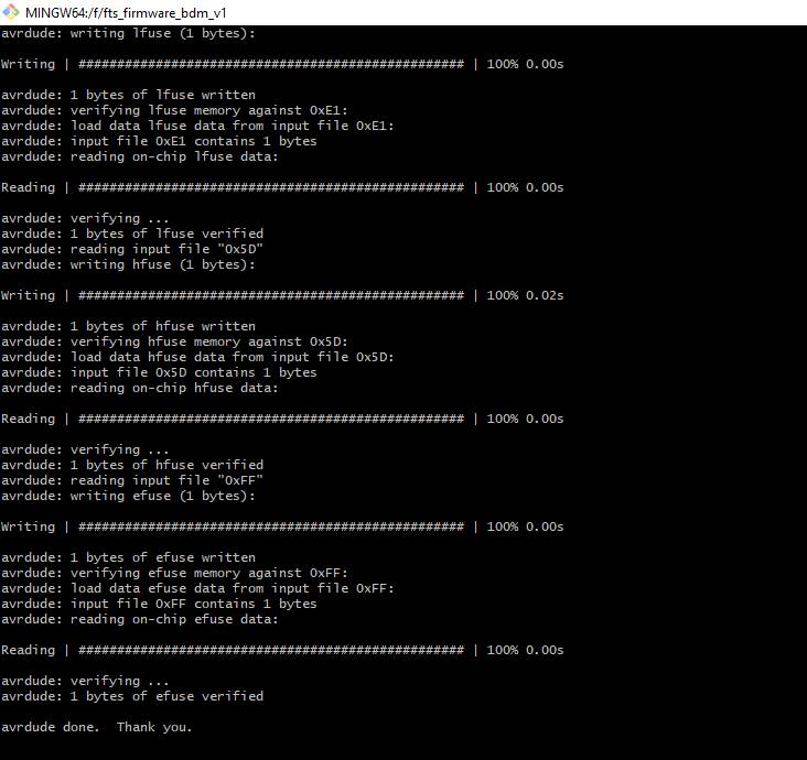
make rstdisbl.
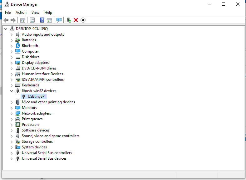
To check that the ISP board is working properly as a programmer, I had my fabmate to perform the commands to program his and it worked properly! Fnally it shows into my Device manager.

