14. Networking
Assignment
individual assignment: ~~design, build, and connect wired or wireless node(s) with network or bus addresses~~
group assignment: ~~send a message between two projects (nodes?)~~
This week we are creating a network with a bridge board and two node boards. I started by redesigning the bridge and node boards using Eagle. In the final iteration, I added a Power On LED to the bridge board and changed the code to make the Bridge board tell us his name.
Making the Network
Node Boards
To completely redraw the nodes for this assignment, I went to Eagle and gathered the parts.
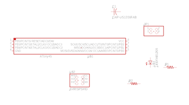
I also dropped in a few VCC symbols.
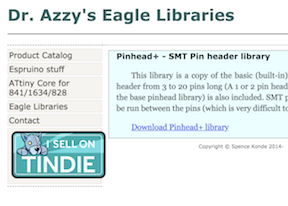
I had trouble finding a 2x2 surface mount part even though I have the PINHEAD Eagle library. I found what I needed here at Dr. Azzy’s Eagle Libraries.
After I got all of the parts, I started making the connections.
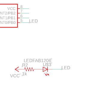
I got a red LED and initially called the connection PB0 because that is where it will be connected to the ATtiny45.
But then I decided to call it LED to designate the connection on the ATtiny45.
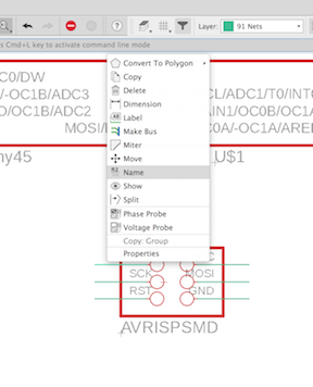
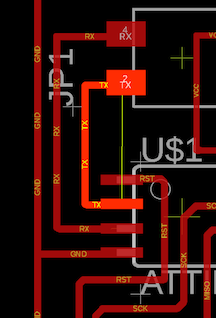
To designate a name for a connection, draw a line with the Net tool and then right click on it to bring up this menu. Then right click to choose Name.
To make the connections for the 6 pin, I call them what they are. I will need to know exactly where MISO is when I go to attach my Atmel programmer.
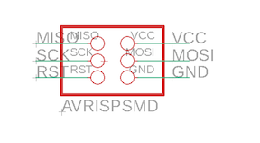
When I’m finished, all of the connections are named.
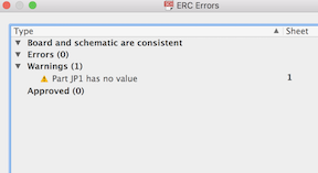
I click on Tools–> ERC to see what ERC has to say about my errors.
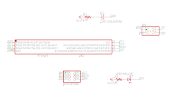
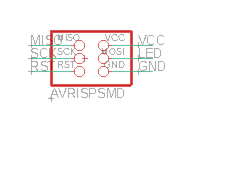
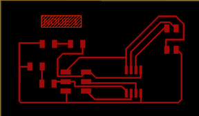
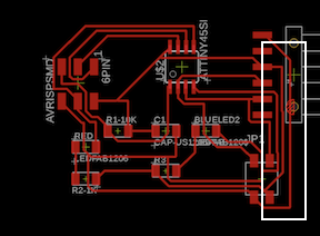
As it is a clear report, I click on the BRD to show the board from my schematic. It’s not as messy as it usually is because there are just a few components.
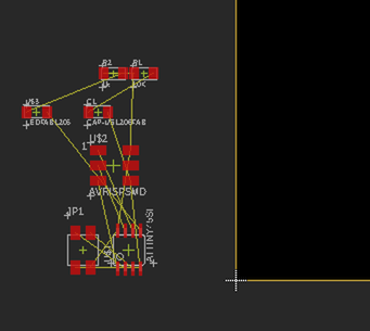
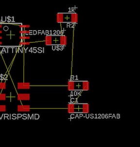
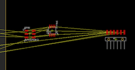
I drag all of the components into the dark black work space on the board and spread them around so I can see what the connections look like.
If you space them out like this, you can see what needs to be close to what in order to make the connections work.
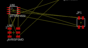
It’s always a good idea to align the 6 pin and the micro controller.
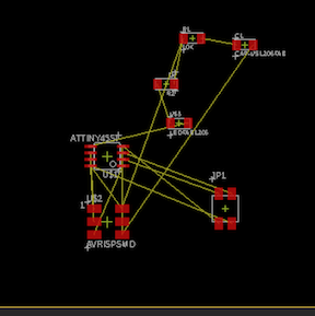
You can see in this picture how interconnected these components are.
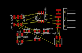
In this picture, you can see the connections between the resistors, capacitor and the LED. If they are located close together, routing the traces will be easier. The capacitor needs VCC on one side and GND on the other. It’s not picky about which is which.
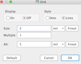
Because I’m having trouble adjusting the location of components with precision, I realize that my grid “Size” is at 50 causing the big jumps in position rather than sliding smoothly. I change it to “2” and it’s much better. I wonder why Eagle doesn’t remember these settings for me?
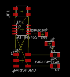
The components are looking fairly well aligned. It’s time to start drawing traces.
I draw a few traces before I realize that they are very thin. I check my minimum trace width settings. Another setting Eagle does not remember.
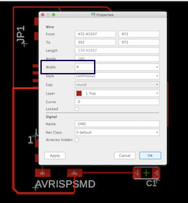
I change the setting to 12 but I have to go back and reset the Properties of all of the lines I’ve drawn. (Right click, choose Properties. It will only highlight a segment of your trace unless you have drawn the whole trace with one go. I can’t usually do that but I am getting better at it.)
This is odd. When I click on the MOSI pad, it is not connected to anything. I must have done something wrong.
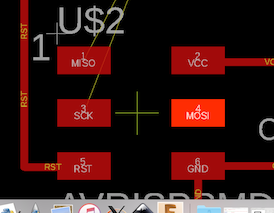
I go back into the schematic view and see that MOSI was LED.
I change it to LED on the 6pin in the schematic and then go back to the board. Now I can connect it to MOSI on the ATtiny45 and the LED.
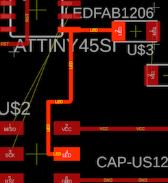
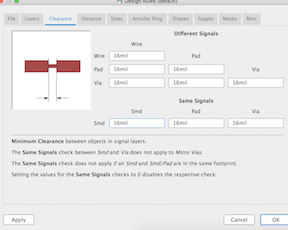
I notice that some of my traces are pretty close together so I remember to check the “Clearance” setting. Those numbers need to be 16.
This is a weird thing that Eagle does sometimes. It says there is no connection when there clearly is one. It’s probably fine. Redraw the connection from the center of the affected pad out to the existing pad and make sure the exact ends of the connections are hit. Otherwise, if you later move things around, you might lose track of that connection.
When I’m finished drawing the traces, I ask ERC if he sees any errors. This report came back clean enough.
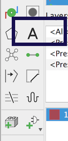
For fun, I give the board a name and designation using the letters. You’ll find a big A on the left where your tools are.
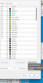
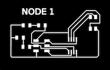
Time to download this board. Go to Layers and hide all of the layers, then un-hide the Top layer.
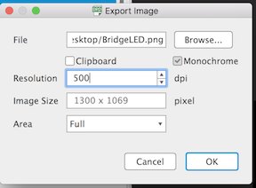
File—> Export-> Image
Be sure you have 500 dpi and monochrome checked.
Open that png file in Inkscape and scale the png down to 52%.
I export the file at 1000 dpi and it’s ready for the mill.
Milling
I milled the boards in the Roland SRM-20. I begin by “modding” the png file using mod.cba.mit.edu. It downloads an “rml” file. I upload my “interior” file and get an rml file for the outline of my board.
Then I use the Modela interface to push the rml file to the mill.
It takes a few minutes to get a nice milling job.
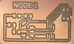
Soldering
After milling the boards, I soldered on the parts. My pre-tin soldering is looking more like paint and less like blobs.
Continue with the network
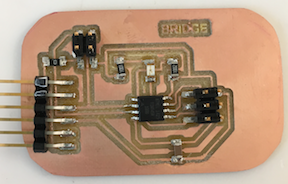
Made two of the same node boards and one bridge board. Well, sort of....
Bridge Board Redesign and Lessons Learned
Redesigning the layout of the boards is tricky. You have to imagine that the way Neil laid them out is the most efficient way of doing that and getting all of the connections correct. Assume, then, that the microcontroller and the 6 pin have to line up because 5 of the 8 microcontroller pins must match up with 5 of the 6 pins of the 6pin connector. That’s just the way it is. So now you can move the remainder of the parts around and, assuming you are not adding anything more to the board, you need to follow a few rules of connectivity. For example, the LED has to be connected to the resistor in a certain order (anode side of the LED toward the resistor). And the FTDI connector has to line up in a certain way because of the order in which those pins occur on the cable. It was that last rule that tripped me up on my bridge board redesign and had me going in circles for some hours.
Sometimes you can change the order in which pins are designated on a component. For example, the 2x2 connector doesn’t care which pin is TX and which pin is RX. You can move them all around because the connector is just a conduit of information. Any of the 4 pins can be VCC, or whatever. You just have to adjust your cable. But that FTDI connector, although it looks like a conduit, it is not. That’s because it is a cable and the cable has a set circumstance. It always goes in order RTS, RX, TX, VCC, CTS and GND. You can tell what direction it goes in because the black wire is GND and the red wire is VCC. So don’t randomly try to re-order those connections in order to make your traces meet up neatly.
Lesson learned.
I remade the bridge board with the same components as the nodes plus the FTDI and programmed it with Neil’s code. Safety net. Let’s just make sure the board works before we change the code.
Make the cable.
You need a four wire and three 4 FCI Header and Wire Housings. They look like this:
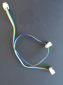
and they get plugged in with the header going across the 2x2, not in line with its feet. You need to keep track of where the wires are going from board to board to ensure that the wires are connected properly.
Imagine that the blue wire is for VCC. That means that if your VCC pin on your bridge board’s 2x2 is outside left, the VCC on your node boards have to be outside left when they are plugged in to this connector. If that doesn’t make sense, just keep in mind that the wires have to line up. I marked my 2x2 male connectors and the female cable connectors with a little dot of WhiteOut so that I don’t plug them in the wrong way.
Edit and program the node boards
The next step requires small edits to the c code file. First flash the bridge board with the c code as it is.
sudo make -f hello.bus.45.make to make the hex and out files.
Then sudo make -f hello.bus.45.make program-ice to program the bridge board.
Before programming the first node, go into the c code (I use Brackets). Where it says #define node_id ‘0’, and change that zero to ‘1’ for the first node board and ‘2’ for the second node board. This change in the c code requires that you go through the process of “making” the hex and out files again.
The best way to keep everything straight is to create a new file folder for the node boards. Put the c and make files in the new file folder. Go through the makefile process to create the hex and out files. Now push the node 1 file onto your first node board. Remember to plug your programmer into the node via the 6 pin and give the node power through that 2x2 pin. Be careful that you are plugging in the 4 pins correctly.
Do the same process all over with the second node board.
Ask the bridge and nodes to speak to each other
After programming the boards with the different node numbers, do this:
- Plug the bridge Board into computer with the FTDI cable to the 6 pin.
- Connect the nodes and the bridge board in a chain with their 4 pin headers. (Did you make that cable first?)
- Open the Arduino IDE and go to Tools>Serial Monitor to open the serial monitor screen.
- Make sure Arudino can see your FTDI cable.
- Set the baud rate to 9600.
- Enter the number of a node into the serial port and “send” it.
- “Node 1” should appear on your serial monitor and the LEDs should flash in order. After all the LEDs light up once in sequence, the board that corresponds to the number that is entered into the serial port lit up again. The message went around in a circle.
Note to self: Get a tripod.
Change the Bridge Board and Code: The Blue Light Special
I think I have learned alot starting with the components of Neil’s boards and moving them around. However, when I was challenged to add something to the standard boards, I changed my bridge board to add an extra (power on) LED.
I started by copying my Network Bridge Project in Eagle so I didn’t have to rebuild the 4 pin, 6 pin and Attiny45 connections from scratch.

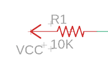
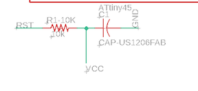
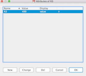
I made one correction from my earlier board by adding VCC between the connected capacitor, 10k resistor and RST.
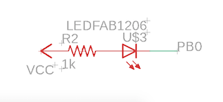
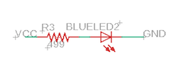
And added the blue LED with a 499 ohm resistor.
I asked ERC to tell me about errors but all he had to say was that many components had no value.
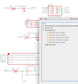
I checked the values, however, and they were there, so I moved on. ERC is not perfect, but he does come in handy.
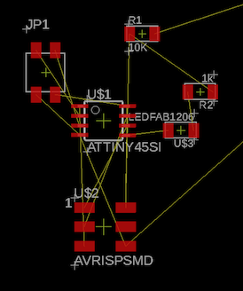
I put the components on the black workspace in the same way I typically do: start by lining up the 6 pin, the micro controller, and the FTDI.
I put the 4 pin on the outside and clumped the resistors, capacitor and LEDs together.
I used SAVE AS and changed the name of the brd file and asked AutoRouter to see what he could do with. (I typically don’t accept AutoRouter’s suggestions so by using a file with a different name, if I didn’t like AutoRouter’s choices, I could just open my old file and draw my own traces.)
After making sure my design rules were set to 16mm clearance and 12mm minimum trace, I clicked on AutoRouter. As you can see, he had a pretty easy time coming up with 5 different 100% routes. He really saved me alot of time this time.
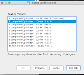
I chose the last of the 5 because it had the fewest number of traces running under the ATtiny45. Once it is soldered into place, it’s nearly impossible to see what’s going on underneath it. I’ve had to remove more than my share of micro controllers trying to debug a connection problem.

I did a little clean-up such as moving the traces straighter where I knew the clearance minimum did not matter (like under the FTDI).
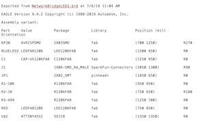
I added its name to the board and exported the file.
I also exported the parts list.
I opened the exported png file in Inkscape and reduced it to the correct size before exporting it for milling. While I was there, I made the letters in BRIDGE bigger and bolder. Then I saved the file at 1000 dpi for milling.
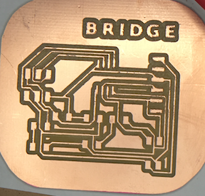
Here’s a short video of milling on the Roland SRM-20.
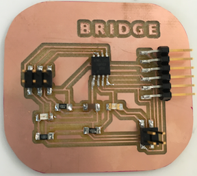
And the product.
I gathered the parts and soldered them on, starting with the ATtiny45.
When it was finished, it was time to program the board and test my LED theory.
The LED Theory
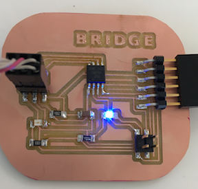
My theory is that the blue LED is connected directly to the VCC port on the FTDI through its resistor so any time the FTDI cable is providing power, the blue LED should be on.
I hooked up the Bridge to the FTDI inside of my Parallels program and the blue light went on!
Programming
Programming went smoothly. I had made a few changes to the code (discussed below).
sudo make -f hello.bus.45.make created the hex and out files
sudo make -f hello.bus.45.make program-ice programmed the attiny45.
But Does it Work?
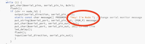
When I put it into the Arduino serial monitor and sent the first message for node 0, the monitor said back “Hey. I’m Node 0” in accordance to one change I made to the code.
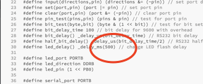
In the video, you might notice that there is a longer delay between the lights coming on due to a change I made in the flash delay.
Blue Light Blinking Node Movie
Files
These are the files for the last version:
Bridge board interior–use inverted