Electronic Production
Week 5 - Electronic Production
Here you will find my work description during this fourth week
Class notes
Assignment
Our assignment for this week is:
group assignment:
- characterize the specifications of your PCB production process
individual assignment:
- make an in-circuit programmer by milling the PCB,
- then optionally trying other processes (ATtiny45, ATtiny44)
Group assignement
For this assignment I team up with Marta, Óscar, Thais, Ilias and Andre.
We are going to create a PCB using the milling process (without chemicals).
The machine used was Roland SRM-20.
Working area: 203.2 (X) x 152.4 (Y) x 60.5 (Z) mm Materials: Modeling Wax, Chemical Wood, Foam, Acrylic, Poly acetate, ABS, PC board Spindle speed : 3,000 – 7,000 rpm Input Format : RML-1, NC code Software: V-Panel
We used FR1 PCB Board from Inventables
PCB Milling process
Model should be a black and white 2D raster file (.PNG) with high resolution.
We took the ones provided from fabacademy archive:


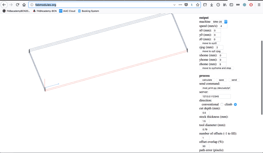
Our Instructors recommand us to start with fabmodules.org. open fabmodules in the browser.
- Check the resolution and the size of the imported file
- As input select PNG ang choose the trace file.
- Select Roland mill (.rml) as output format
- Process is PCB traces (1/64)
- Choose Roland SRM-20 as machine
- Change machine setting as following - x (mm) y (mm) z (mm) and xhome (mm) yhome (mm) are all set to 0 - zhome is set to 5 or greater (move up the tool at the end of the process) - tool diameter : 0.4mm (means 1/64 inch)
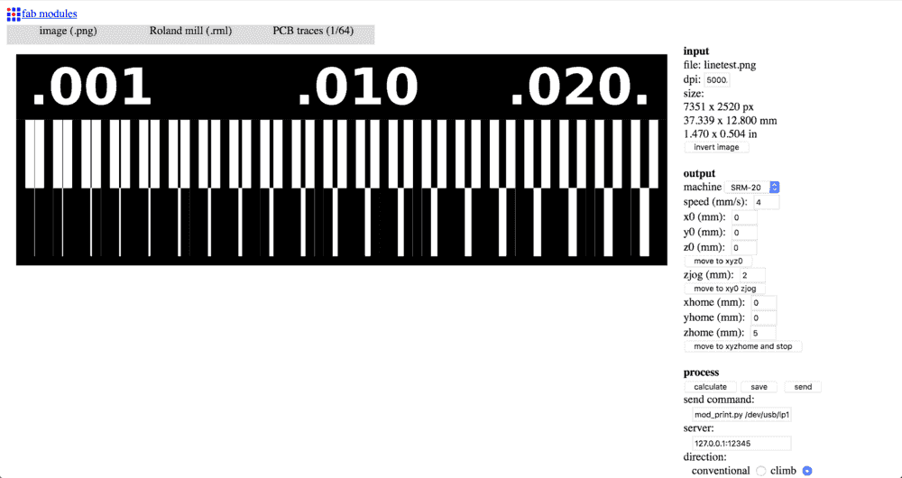
- Calculate
- Save rml file
- install PCB using double side tape on “cleaned” surface
- Turn on the machine (Machine should find its origins z, x, y)
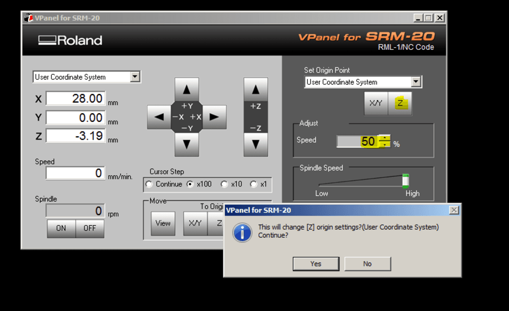
- Run V-panel software
- move to your desired X and Y origin, then select Set origin point X/Y (right panel of V-Panel software)
- install tool, then slowly move cole to pcb
- unscrew tool and gently (with your fingers) let it touch the pcb, then screw it again
- Now set origin point Z
- move up the tool (carefully )
- be sure spindle speep is set to miximum
- be sure speed is set to 10%
- click cut, a new window appears
- Delete all files
- Add rml generated file
- Click output, process starts immediately
- if cutting is Ok you can increase speed (max 70%) - 50% recommanded
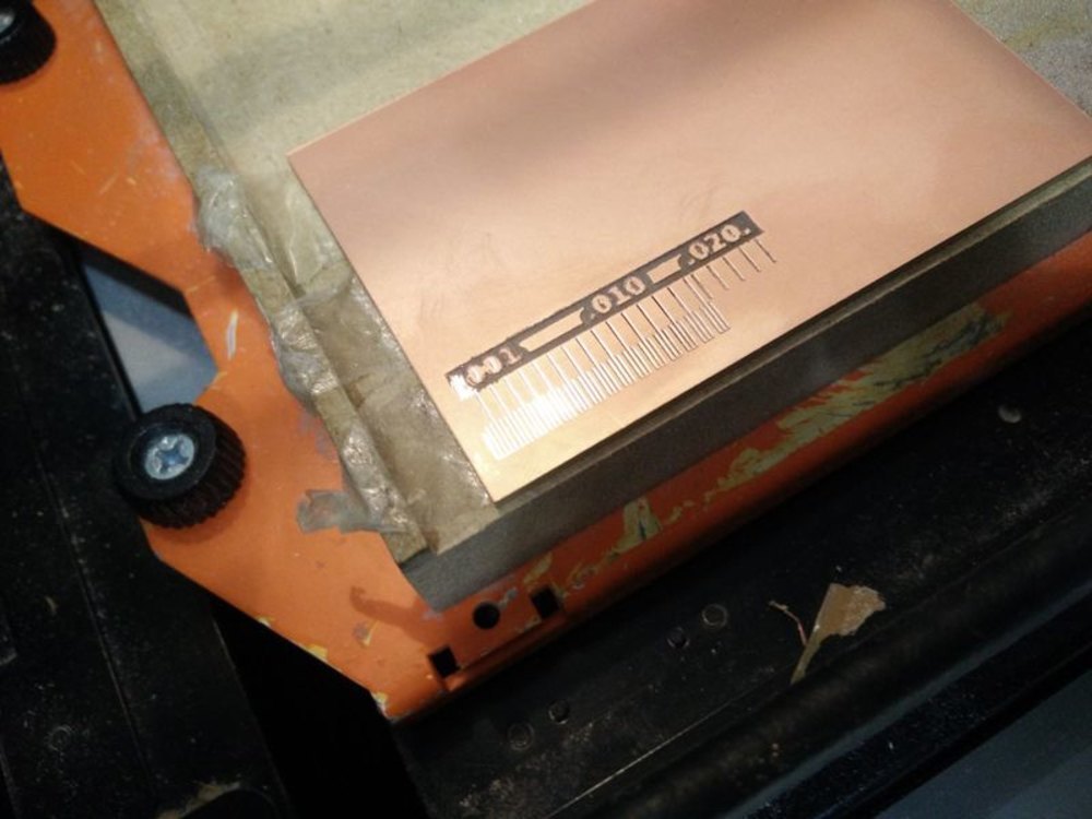
As you can see the cut was not deep enough, this is probably because the board is bended and we didn’t set the Z origin at its lower point.
Make Z again (lower), and mill again.
Follow the same process for outlines (chainging process in fabmodules and tool obviously)
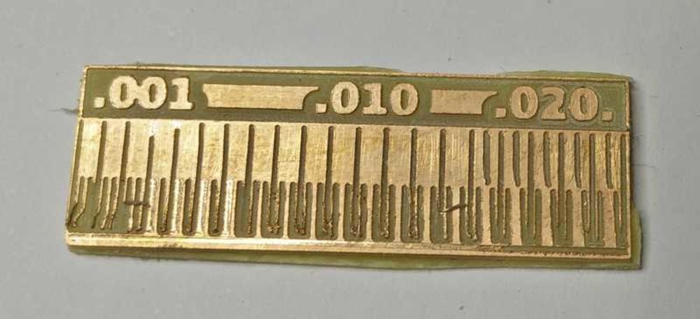
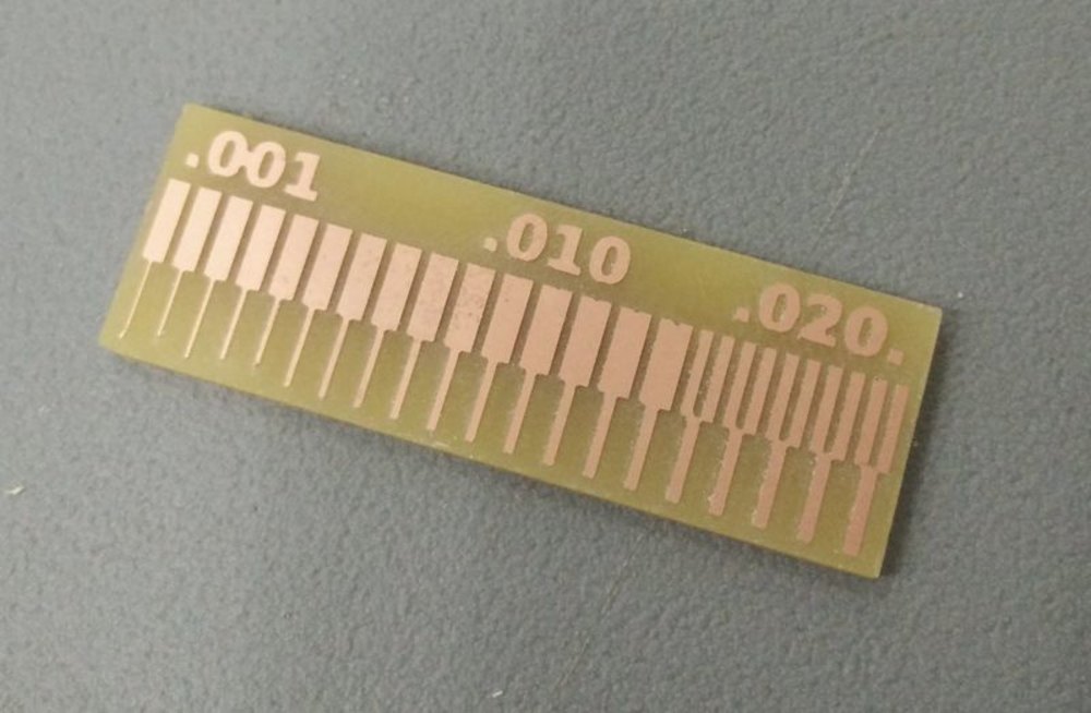
Final result:
Conclusion:
- it’s not that hard, but we need to be really carefull to prevent breaking fragiles tools.
- we had an issue with the outlines cutting (one side had not been cut), we manage to fix it flipping the model, and do the process again, but we should double check the 3D view of the generated toolpathes.
- be carefull of the bended board and the Z origin (you could increas the cut depth in fabmodules)
- check everything before removing the board, after it’s too late (and you may finish with a knife as we did).
- be carefull of the tiny parts of copper on the board, you may cut your finger as Illias did. clean the board with an appropriate tool (like cutter blade).
This is the board another group did, with better results:
Individual assignment
Neil asked us to produce a FabISP, there are several versions of it. I chose the “neil’s version” with ATtiny44, you can see bellow.

There is a tutorial, original verion by Ana Kaziunas France updated by Eduardo Chamorro under licence CC-BY-NC-SA.
This tutorial let me have a a global view and a line to follow for this assignment.
Model
I decided to change the model a little bit usung Inkscape, but first open the provided module in fabmodules to note dimensions.
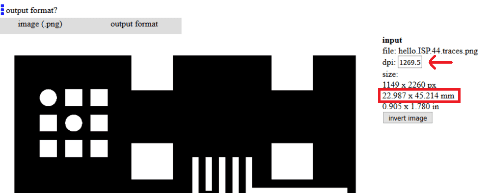
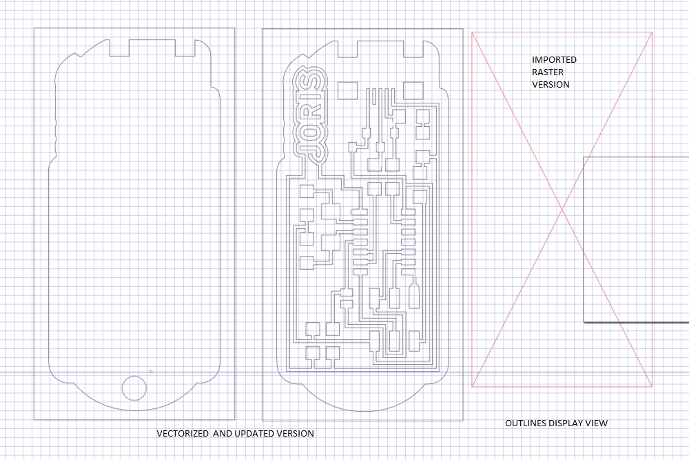
then I import module to Inkscape, vectorize it, and start editing making the global shape a key holder.
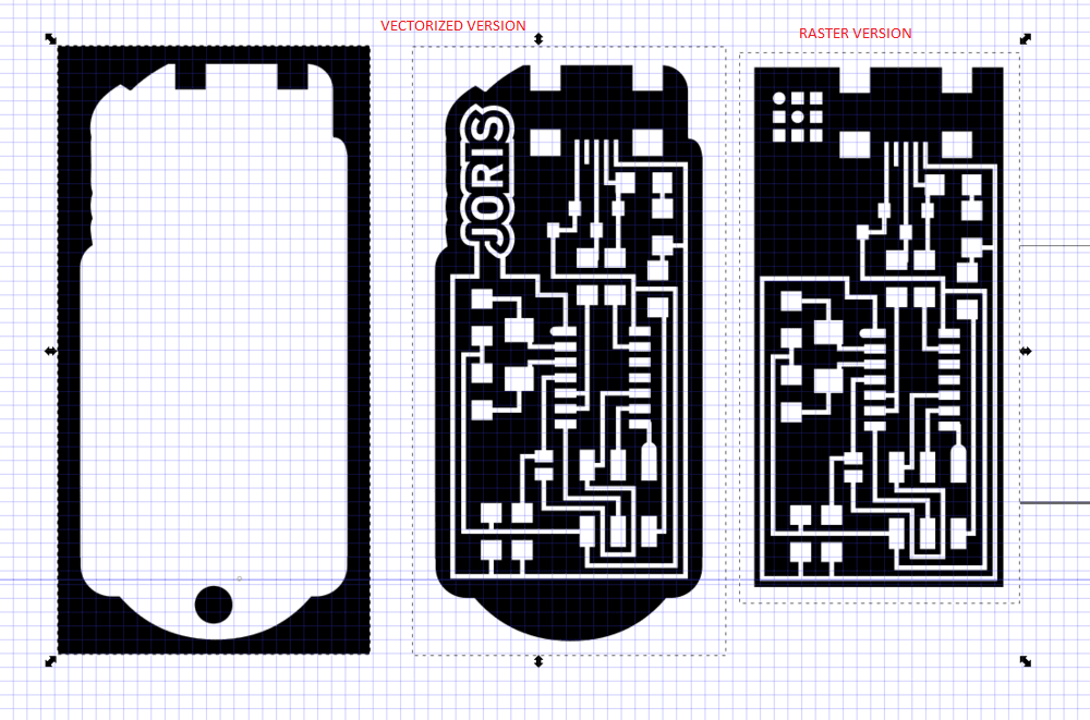
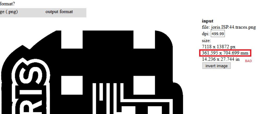
Let’s go back to fabmodules to check new model dimensions. And boum. wrong dimensions.
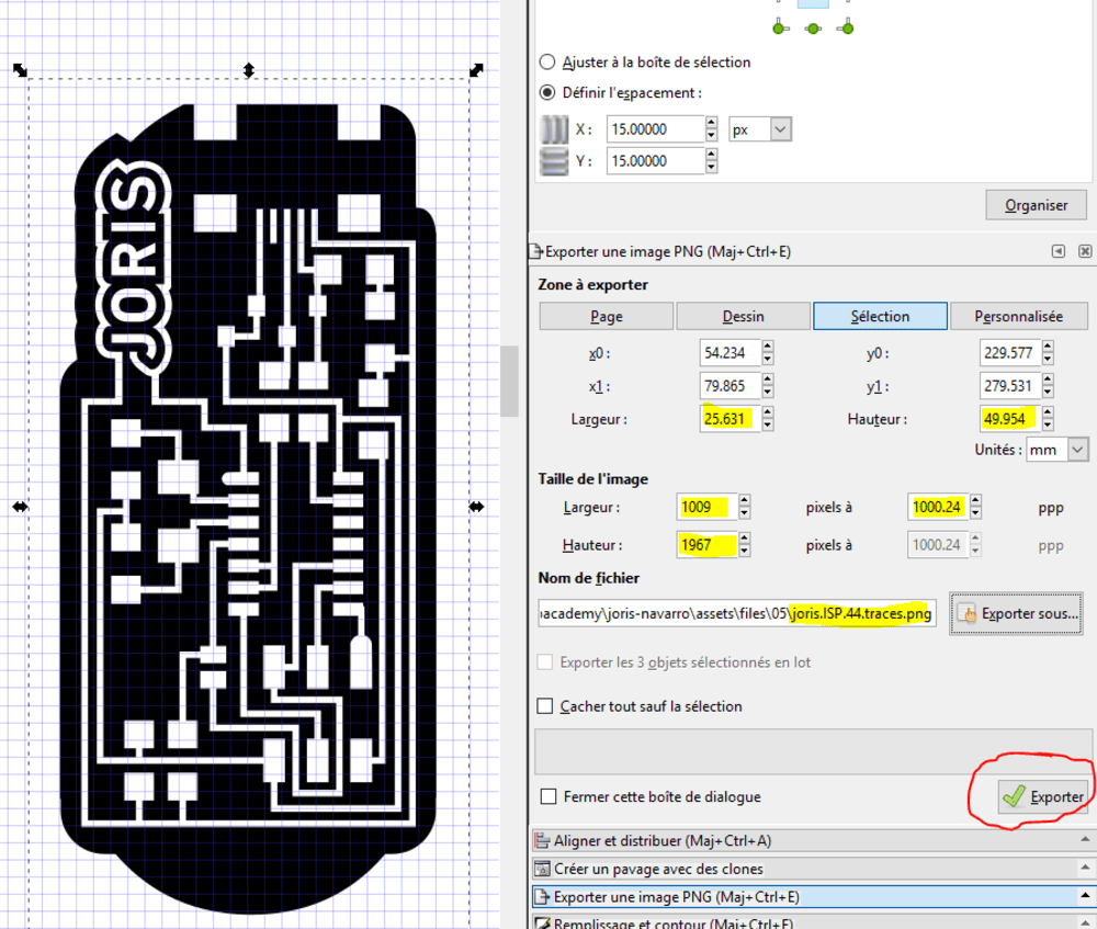
I missed something. Finally the imported file has not in good dimensions, so I scaled according of the proper dimensions and updated png export settings to export a good image and desired resolution.
Once confirmed with fabmodules/mods we can start using it.
FabModules
FabModules looks simplier than mods, so let’s start with FabModules.
Traces
- First step import you PNG file in input format menu and check dimensions.
- Then select the machine you are going to use in the output format menu, Roland mill for me, in order to generate the good output format.
- You can now select the process in the process menu. We are going to mill the traces first using 1/64 inches milling bit.
- choose Roland SRM-20
- set origin at x=0, y=0, y=0 because we will define origin using the machine software.
- check setting “cut depth parameter” = the thickness of the copper layer (0.1mm)
- check setting “tool diameter” = 1/64 inches = 0.4 mm
- check setting “nb of offsets” = number of pathes around a trace (4)
- check setting “offset overlap” = 0.5, this mains that the next path will run 50% of its diameter (0.2mm) over the previous path. 0.4+0.2+0.2+0.2 = 1mm around trace.
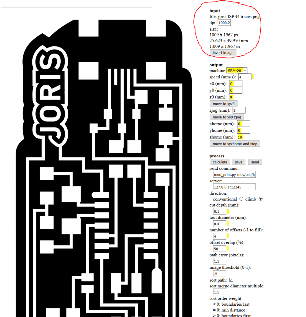
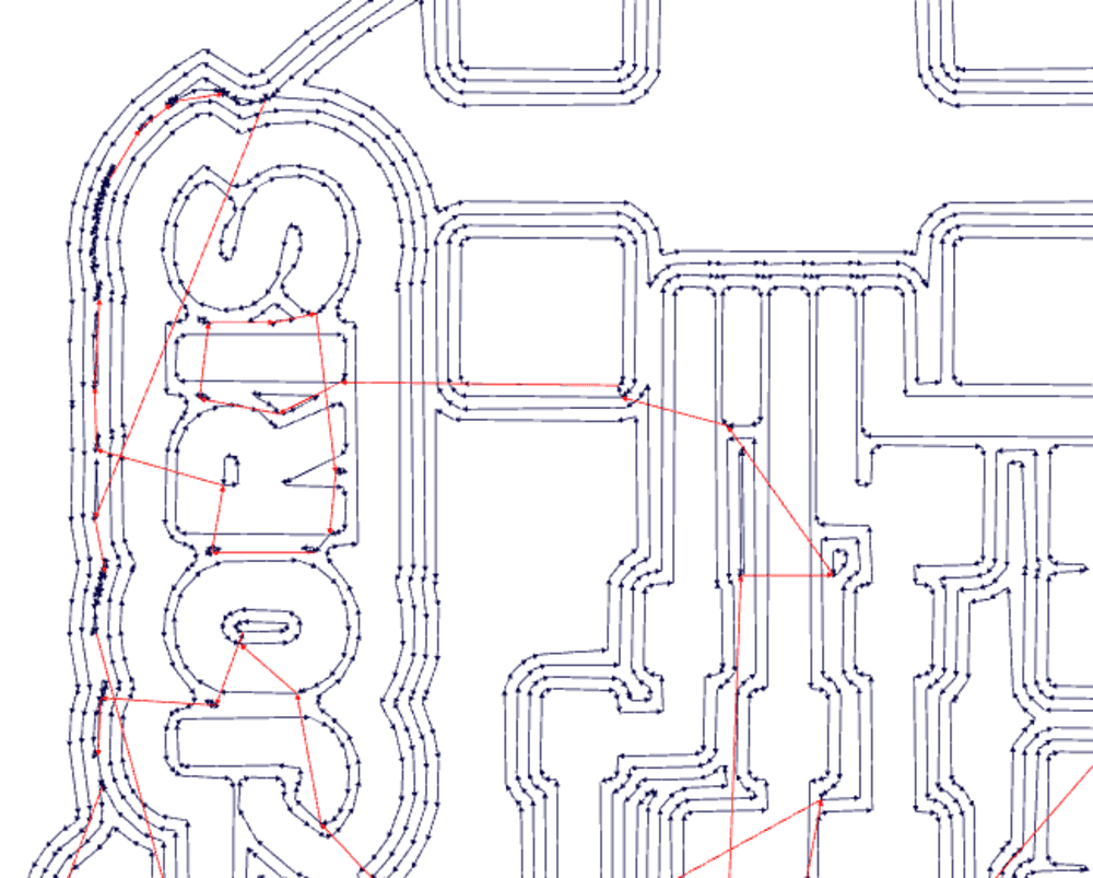
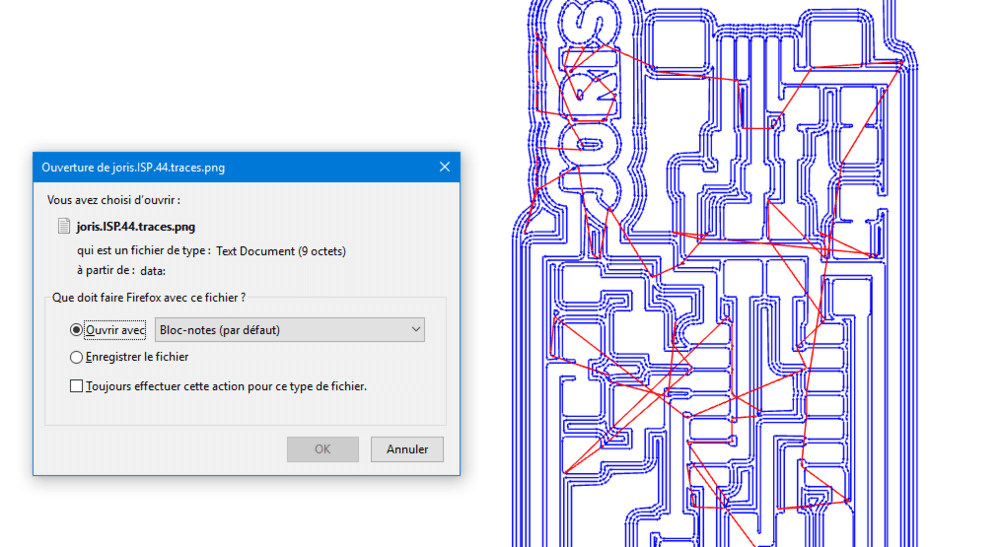
- click calculate to view pathes. Check everything is going OK
- Click Save and put generated .rml file in the cloud.
Click here to download the rml file
Outlines
Now we are going to cut the board according to the shape we defined before. The process is similar until the “process menu”. Here you have to choose “PCB outlines 1/32” bacause we will cut the board using the 1/32 inch milling bit. Set machine to Roland SRM-20.
Use the same origin (0,0,0) and home (0,0,10). To be less agressive let’s set the “cut depth” parameter to 0.5. We use the callipper to measure the thickness of the board it indicates 1.5mm, so we set “stock thickness” parameter to 1.5.
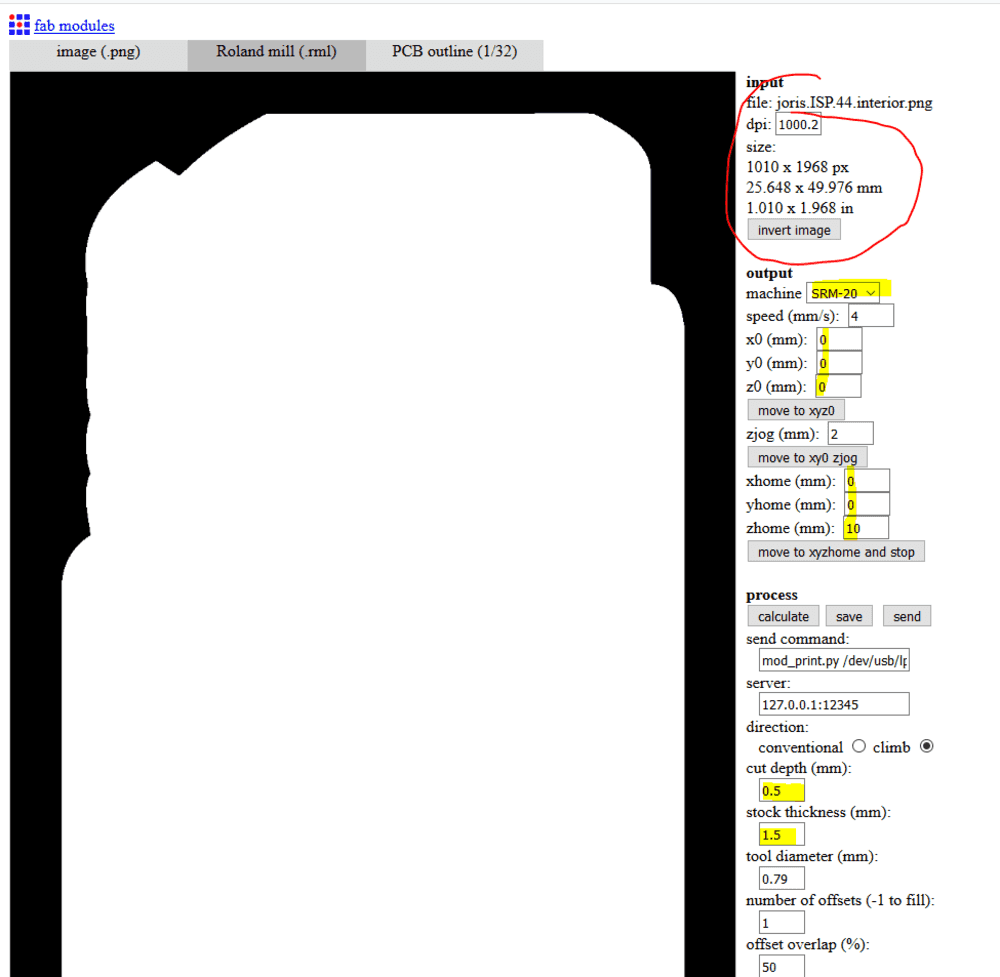
Click calculate, check the pathes, and then click Save to store the generated .rml file.
Click here to download the rml file
Mods
Let’s give a try using Mods !
- Open Mods
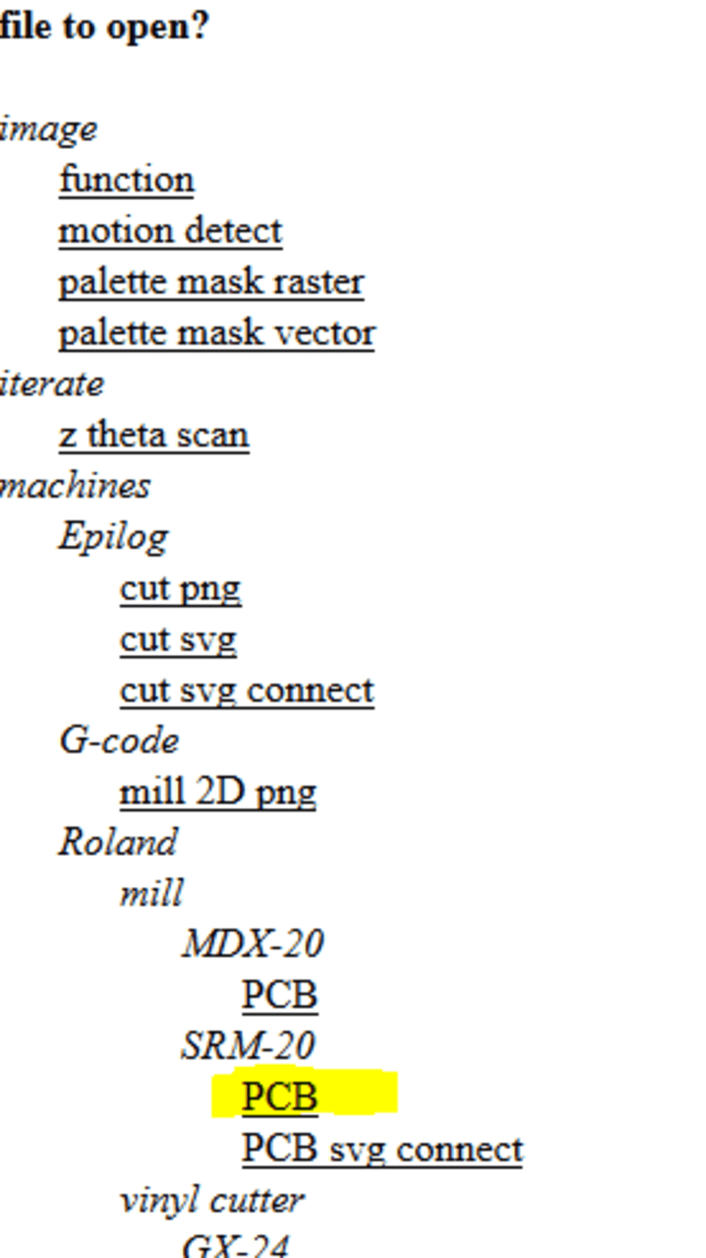
- in the “programs” combobox select “open server program”, then choose machines » Roland » mill » SRM-20 » PCB as shown bellow
- open your PNG file.
- open trace PNG file, and select “mill traces (1/64)
- Change settings like we did in FabModules (in yellow in the image bellow)
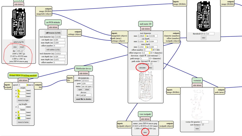
- then click Calculate in the “mill raster 2D” box. A new tab will open and show you the generated pathes. But I would like to have the .rml file.
- Let’s add a Save box. In modules combobox select “add server module”, and choos, “file » save” module. A new box called “save file” appeared. Go to “Roland SRM-20 milling machine” box and click on the output (outputs file), then click in the “save file box” input (inputs file (object)), you can see a new line that relies thos 2 boxes.
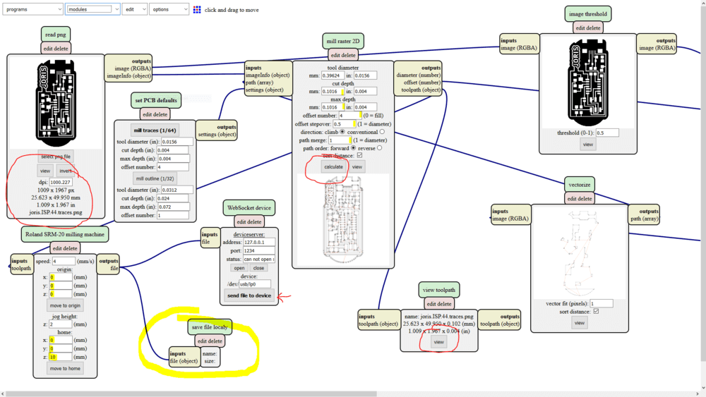
- click calculate again, and now a dialog box invites you to save the generated .rml file ! Store it to the cloud.
Click here to download the rml file
- Do the same with you outline PNG file, but remember to change the process in “set PCB default” bos to “mill outline (1/32)”
- change parameters, and click calculate.
- Check pathes and stor generated .rml file.
Click here to download the rml file
Milling
Once we have ours code machine files we can now start the milling process.
The sacrificial layer was already installed and fresh surfaced in order we can start using machines on flat level.
I know MDF is not the perfect sacrificial layer due to humidity, but it will not be affected in the time lapse between the surfacing process (morning) and milling process (afternoon).
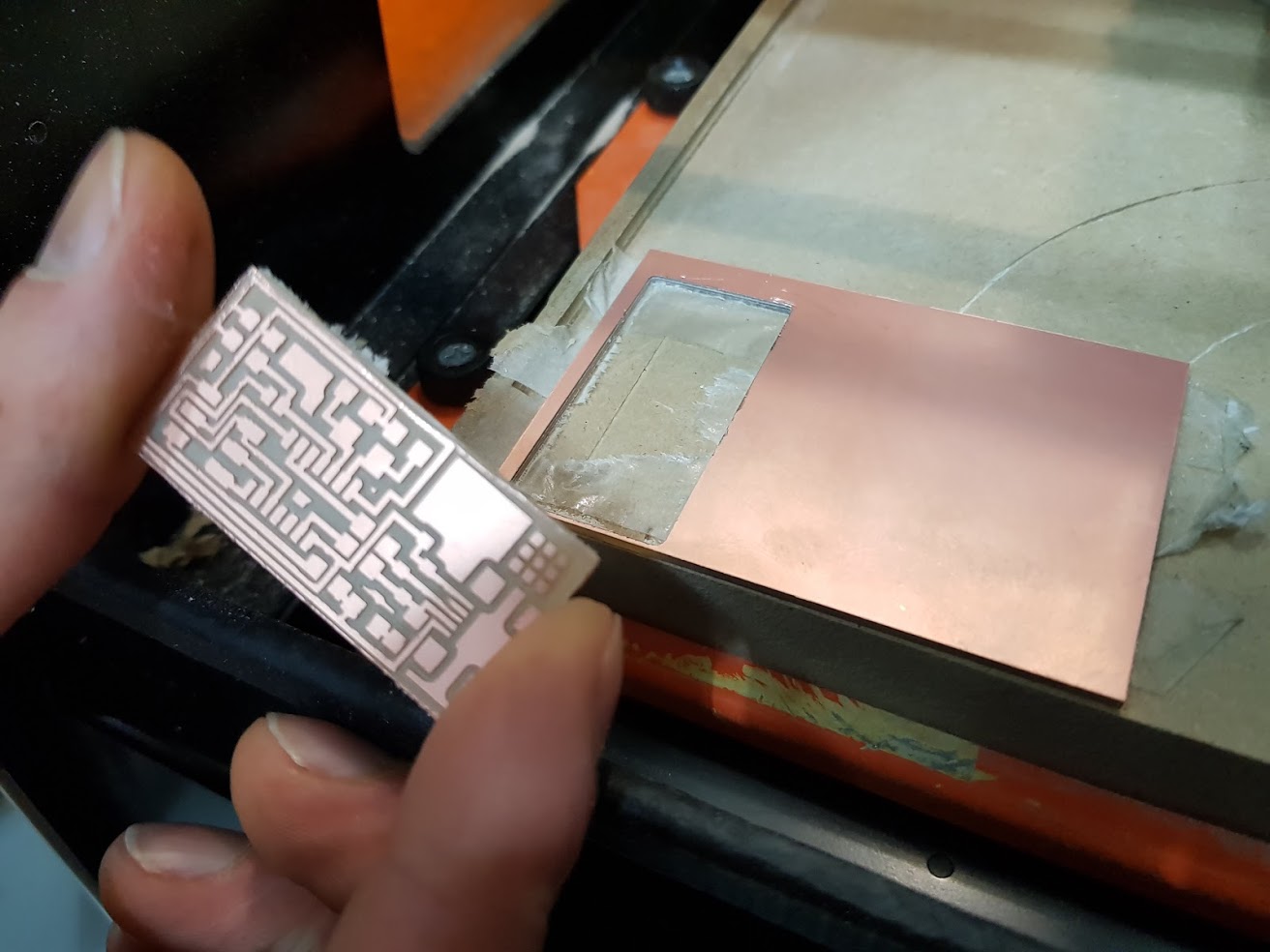
- We have to clean it using alcohol to remove all dust and lasting glue on it. Before gluing the board we can check its flatness using a ruler.
.jpg)
- Install 1/64 milling bit. I prefer put something soft on bottom in case of the tool falls down.
.jpg)
- Set origin, move the tool to your X and Y origin et set origin using the Roland V-Panel Software. Button is on the right side. Then move slowly and carefully the tool on the Z axis near the origin (like 2-5 mm on top). Then again carefully hold the tool with one of your hands and unlock the tool in order to let it tounch the board. Then lock/screw the tool. Now you can set the Z origin. Once done move up the tool.
.jpg)
-
Set the milling speed (the one on the right side, the left one is the spindle speed, do not touch) to 10%.
-
Load your rml file using “Cut” button. A new window appears, delete all files and add yours. Be aware that when you will hit the “output” button the milling process will start. When you are ready, click “output” and watch.
-
If everything is OK, you can increase the speed carefully until 70% (max). The wait a few minutes to check if the copper layer is cut.
Unfortunately, as you can see, my layer was not cut propoerly.
.jpg)
I need to adjust the Z to fix this problem. Santi showed us how to do it. We have to turn on the spindle and very cautiously move the tool until -0.05 mm (depending on the depth you to fix). Set again the Z origin and move up the tool.
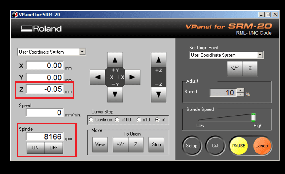
Now you can restart the process. Check again a few minutes later. And if it’s not good repeat the last operation.
- When it is done, change the tool, use the 1/32 milling bit, set the Z origin (do not change the X,Y origin). Load your outline rml file and cut the board.
You should have the board milled like this.
.jpg)
- Time to remove the board and to clean it. First with a blade, then with a “iron cutton” and finally with alcohol as shown bellow.
.jpg)
.jpg)
.jpg)
Soldering
BOM
According to what I read we need the following components
- 1 ATtiny 44
- 1 Capacitor 1 uF
- 2 Capacitors 10 pF
- 2 Resistors 100 ohm
- 1 Resistor 499 ohm
- 1 Resistor 1 Kohm
- 1 Resistor 10 Kohm
- 1 2x3 pins header
- 1 Mini Usb connector
- 2 jumpers (0 ohm resistor)
- 1 Crystal 20 MHz
- 2 Zener diodes
- 1 Usb mini cable
- 1 6 wires ribbon cable
- 2 6 pins connectors
I picked up the components in the FabLab Barcelona stock and put them on double side tape, print the schemas, and I am ready to solder.
Solder
Get ready to solder.
.jpg)
Remember to clean the board using alcohol.
.jpg)
I use an antistatic wristband and antistatic carpet
.jpg)
Here is a video on How to solder SMD:
- put a little bit of solder on one side of the smd component to soler.
- Use tweezers to place the component over the solder you just put.
- hold the component and heat the solder until it “goes around the component.
- remove the iron, the component should stay in place.
- then solder the other side
Be careful of the order you will solder the component, it could be difficult to access some of them, and you could over burn some components. It also could depend on your hand side. Remenber you can rotate the board to have an easier access to the components.
.jpg)
The hardest part was the MiniUsb connetor that has to be perfectly placed due to its tiny legs. The material of this connector is also longer to heat.
.jpg)
.jpg)
.jpg)
Finally let’s do some continuity tests using multimeter. By the way
.jpg)
Smoke test
Plug the board using the AVR programer of the fablab, if you see a green light that idicates that the poxering of your board is OK.
.jpg)
Programming
I followed the documentation documentation on the fabacademy plateform.
Installing software on linux subsystem for windows (WLS)
sudo apt-get install flex byacc bison gcc libusb-dev avrdude
sudo apt-get install gcc-avr
sudo apt-get install avr-libc
download and unzip firmware
mkdir isp
cd isp
wget /2018/labs/barcelona/students/joris-navarro/assets/files/05/firmware.zip
cd fabISP_mac.0.8.2_firmware/
Edit the Makefile
nano Makefile
check that you are ussing the good programmer you should comment the line ‘#AVRDUDE = … -c usbtiny … AVRDUR = … -c avrisp2
but after when you want to use your fab isb you shoud uncomment the avrisp2 and uncomment usbtiny
check microcontroller here is attiny44 and crystal value
Plug avrisp to your fabISP and plug avrisp to your computer
make clean removes main.hex
make hex
then plug your FabISP to your computer using the USB to mini USB cable.
make fuse
Usb was not recognized : unable to initialize libusb: -99
After some investigations, it appears that the Windows Linux Subsystem (Ubuntu) does not manage external USB except FAT devices.
2 choices : Use windows, or find another linux.
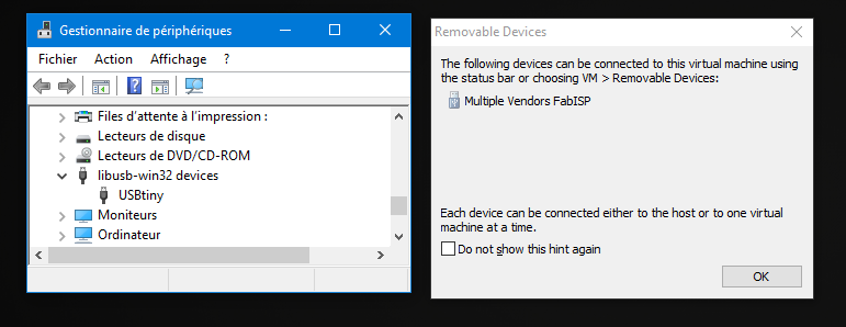
I use a Virtual Machine under Linux Mint Cinamon I set up to test antimony.
I repeat the previous commands and that worked like a charm.
now I can do last command
make program
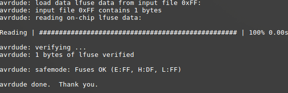
BUT the device is not listed on the system and the lsusb command doesn’t dow it.
I finally found some advices on Bryan’s tutorial, under the “Test the USB Functionality” chapter. I think my problem is between the usb connector and the controller. Bryan suggest to check zener diode orientation, that I didn’t check before soldering. And that was the point, I didn’t pay attention of the orientation of those diodes. And one of them was soldered backward.
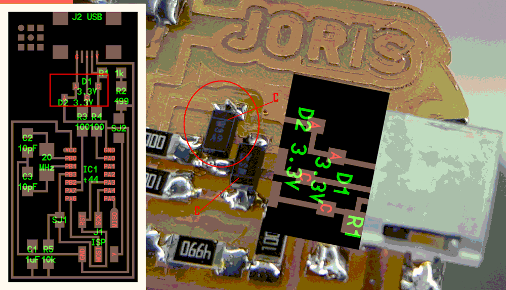
So I unsolder the diode and solder it again respecting the line that indicates the Cathode.
lsusb
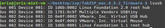
And it works !
Then finally I removed the zero resistors and check again if the board is recognized as a USBTiny device.
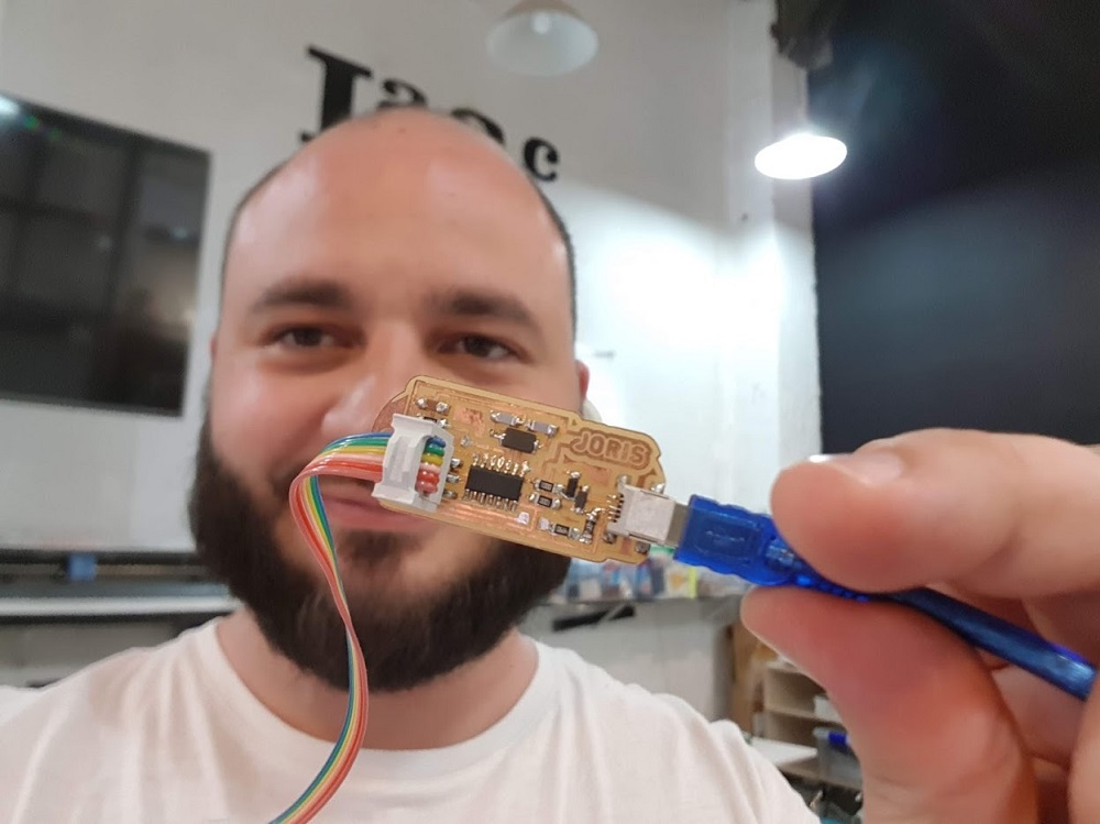
Here is an hero shot of the board, and its smily designer ;)
Stay in touch
Hi, I'm
Joris Navarro, from Perpignan (France), a proud dad, a fab director/manager, a teacher, a ceo, a FabAcademy student, but not only. Click here to know more about me.
Check my work for FabAcademy on FabCloud GitLab
@joris.navarro.
Want to say Hi ? Please send me a message.