Electronic Production
Week 5 - Electronic Production - NOTES
General info
Things to do
Questions to ask
Useful resources
Assignment
Raw class notes
Weekly reviews :
- Saba ghole from USA BOS Earth FabLab
- eunice lee from seoul
- Dario from siena
- yousef alsenwar from Dhahran (nice project : troller)
-
Jacob Jose from Kochi
- Nicolas de COster (ULB) generates a openscad file using js, for pressfit and flexible kits. He also use HP-GL protocol to print directly to the plotter.
class : producing electronics
make an incircuit programmer
PCB boards
SDS is bad, ecthing could be usefull if you produce a lot of circuit in the same tank, but we are be more responsible
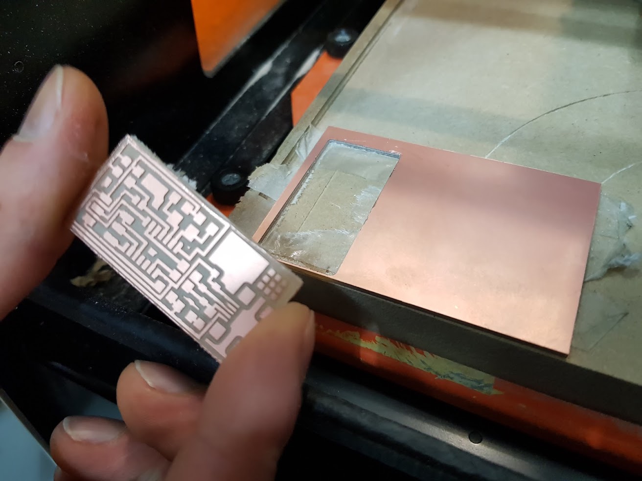
using milling machine
milling produce a small amout of wastes, just dust
precision milling machine really small tools will be used (0.01in is 19$ carbidedepot.com)
if you use weel making a board is less than 1$
we use 2 sides tape to avoid board bending
sacrificial material (layer) under the board to cut the board, that has to be replaced
evrithing needs to be clean
zeroing is important because we will cut only 0.01 in don’t let if fall to the material hang it with your hand when you tighten be sure your tool is not broken clean with a stainless steel rule wash the board with clean water befor assembling the circuit
using vinyle cutter
honghao deng made a cube for fun and create e 3D circuit even multilayer flexible circuit see video bas add that we can use textile vinyle instaed of epoxy Neil doesn’t recommand to start with this but
using fiber laser
40k$ machine can remove the copper
using printer (special)
plating
rfid tags are usually print and ink
enbroidery/sewing
using conductive wire
boards
FR4 are the common ones (greeninsh color) but made using epoxy glass you can’t mill FR1 are the ones we use in fablab (phenolic)
boards are specified by height 1.0oz means 35um (micrometer)
pcb.ng is a online service for fabricating boards (board houses) http://aqs-inc.com/ looks interesting
think and tinker sells the machine that allows you to make your own pcb
seed studio is good
design rules spacing 1 mil = 0.01 in layers 1 side traces on 1.5 use zero resistor 2 sides 4 sides, power layers and ground layer
vias, to connect layers rivets are a clean way to make vias
Vendors https://octopart.com/ is the main provider ? (not sure)
Neil hate breadboards ;)
better mill a final form board
Soldering
they point is shiny and smooth joins (it’s hard to find the god temperature
remember to wash your hand before touching the solder
for smd use tweezers
Order matter, go to the bottom to the top
desoldering braid is usefull for desoldering or heat gun with special tip the point is to hold the piece you want to remove with the breezers and use the heat gun to let the board fall away on the table
pic and place machine is for at least 100 boards it make sense (will be common in labs)
encapsulation (silicon, nail polish)
go to bas (2012 student) molding and casting assignement
CAM
formats
the most common is Gerber we wille use images PNG (much cleaner than jpg) in high resulution (at least 500dpi better 1000dpi)
Mods is the new version of fabmodules
Jon dev his own tool
Have to try this tool too
there will be a recitation on it
Assignement
Group assignement
- caracterize your PCB process (cleaning, setup, underlayer, …)
- create a FabISP see Ali page for discovering what is happening on the programmer
See the brian’s page
practice your soldering until you have tiny shiny smooth joints

Don’t plug directly to your computer, use an extension cable
Extra : try to program the board, in 2 weeks we have to modify the board
Visual inpection this week
Stay in touch
Hi, I'm
Joris Navarro, from Perpignan (France), a proud dad, a fab director/manager, a teacher, a ceo, a FabAcademy student, but not only. Click here to know more about me.
Check my work for FabAcademy on FabCloud GitLab
@joris.navarro.
Want to say Hi ? Please send me a message.


