Week06 Electronics Design
This week focuses on understanding electronics fundamentals, learning how to use electronic test equipment, and designing a custom micro controller development board using KiCad (Installing).
Week 06 Outcome
By the end of this week, I expected I will learn the following checklist:
- Use lab equipment to analyze embedded boards.
- Understand fundamental electronics principles from shared resources.
- Design a micro controller development board in KiCad software after downloading installing and use d/t addons.
- Apply design constraints correctly and draw initial sketches.
Reminders from Rico
- Update DAYG & Nueval
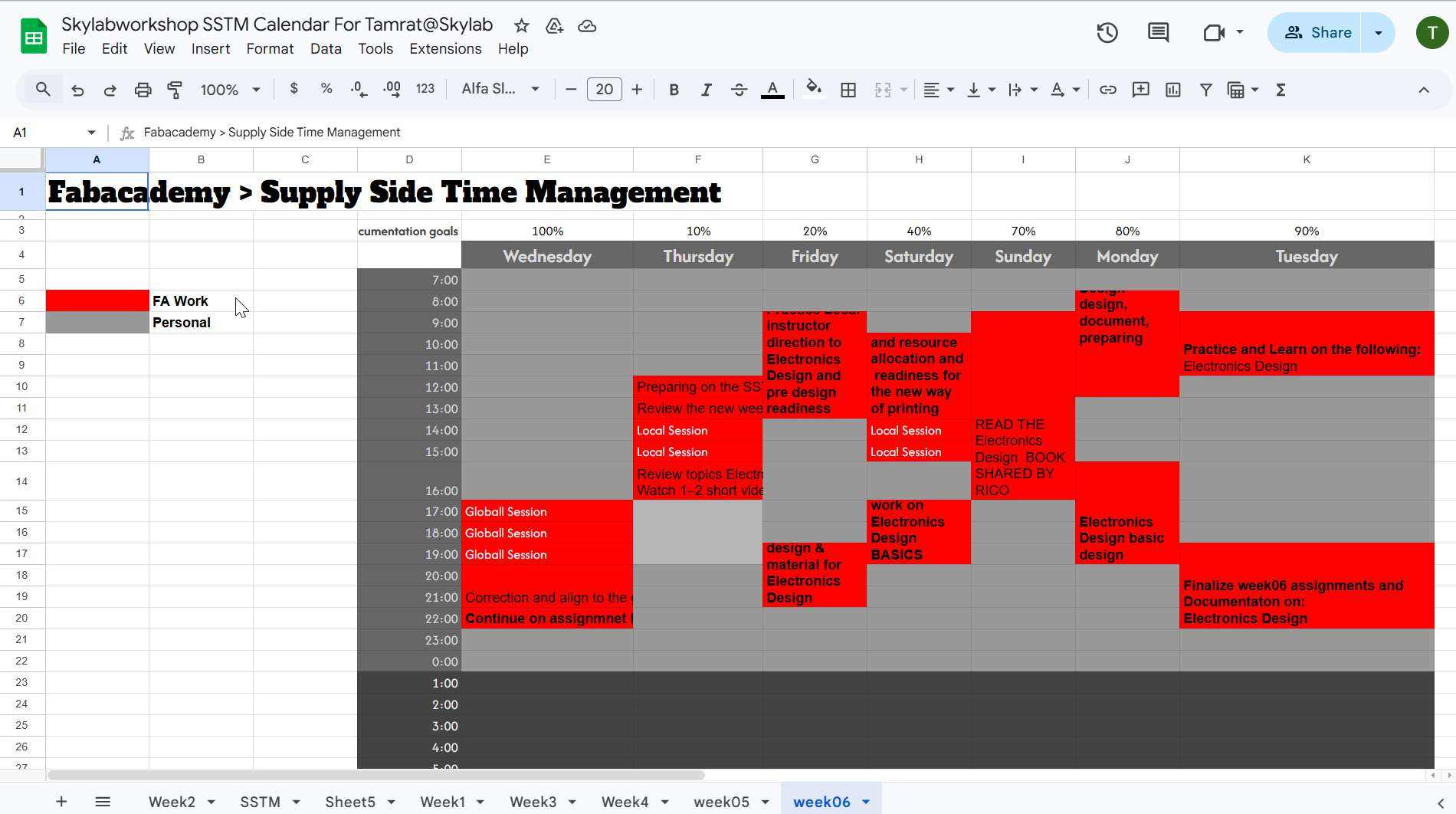
- Update SSTM
- Update Final Project Progress & Tracking Page
- Using the shared resources like book and videos to undertand electronics design
- Download and start using Kicad https://www.kicad.org/download/windows/
- Maintain proper documentation & communication
Local session week06
Unlike previous weeks where the focus was mainly on programming embedded systems, this week shifts toward hardware design — understanding, measuring, designing, and producing the physical circuit board that runs our code. I learn from the session fundamental of the electronics design and methods, softwares and tools used in the process.
Shared resource to learn basics of electronics design
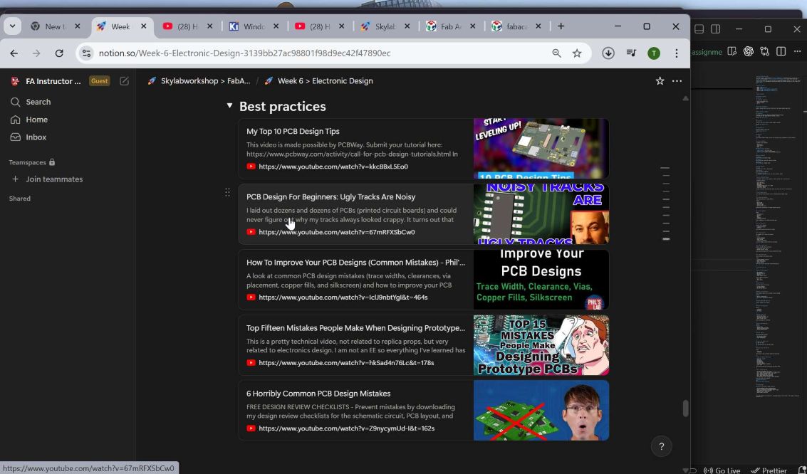
Some session local class on the electronics design with Rico
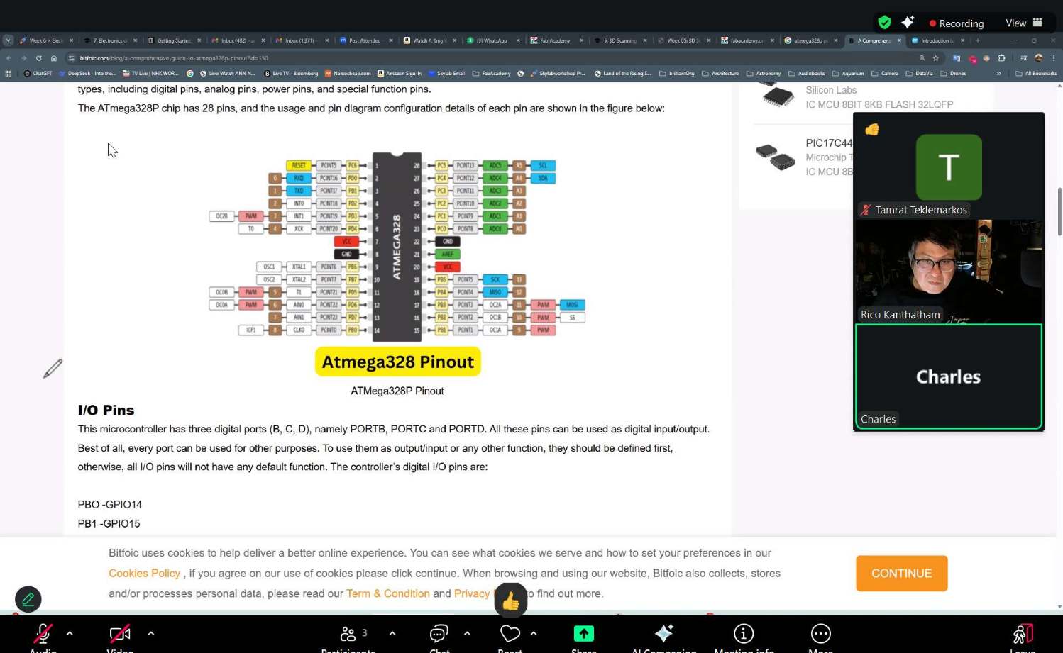
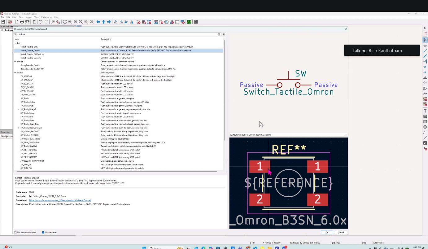
Key Concepts from Getting Started in Electronics
By Forrest M. Mims III Source: local instructor, Rico This book is the fundamental and basic for somen who started from the bottom to understand and work with electronics design, the following is something I learned.
DIRECT CURRENT (DC) ELECTRICITY
Direct Current (DC) is electricity that flows in one direction only.
It may be steady or pulsed, but it does not reverse polarity.
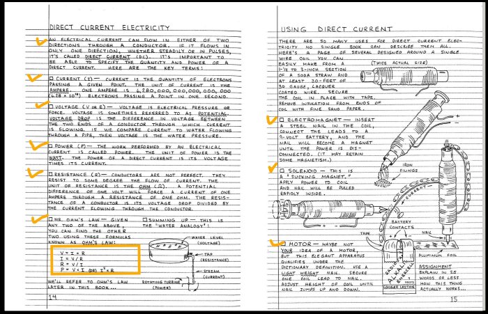
Personal Understanding
This section helped me understand that:
- Electricity is not only energy — it is also information https://archive.org/details/getting-started-in-electronics/page/n27/mode/2up
- Signals are controlled patterns of voltage over time.
- Noise management is critical in PCB design.
- Pulses and waves form the foundation of digital electronics.
Group Assignment (on progress)
Group assignment (link wil be available soon) here it is: week06 Group assignment
Individual Assignment
The following is concept but the full process will be uploaded after installing Kicad
Objective
Use an EDA tool (KiCad) to:
- Design a development board
- USE Kicad to produce it (PCB)
What is a Development Board?
A development board is a PCB designed to simplify working with a microcontroller.
It typically includes:
- Power regulation
- Power LED indicator
- Debug LED
- Reset button
- Programming header (FTDI / ISP / UPDI)
- Extra GND and VCC pins
- Communication headers
It makes prototyping and testing much easier than using only the bare microcontroller.
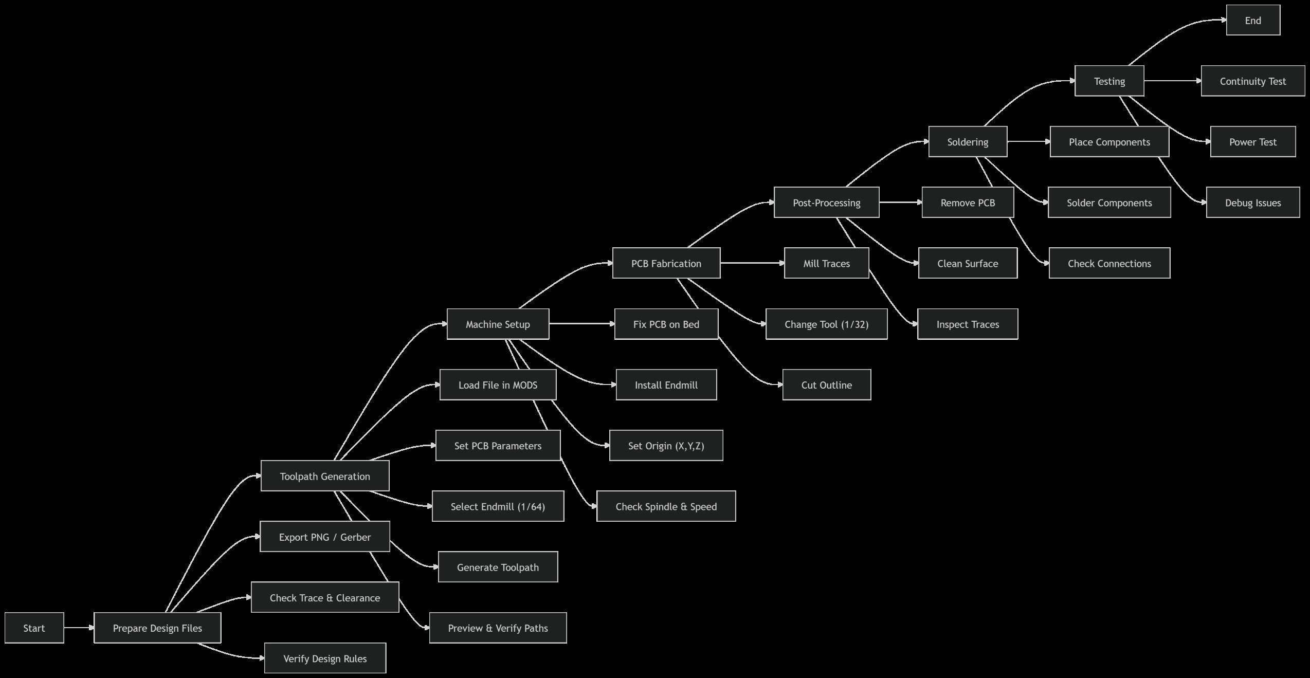
Circuit Design Workflow
This structured workflow ensures a correct and manufacturable board design.
I started working on the paper after my local session with Rico on MCU, ESP32C2 for fabacademy inventory please refer to this … https://inventory.fabcloud.io/?purpose=Electronics%20Design
Generated with AI (Copilot) prompt “change the following to work flow diagram”
Define Functionality:
Clearly describe what the board should do.
Examples:
- Blink an LED
- Read a button
- Send serial data… digital and analog pins …
- Control a motor or other design concep
- Interface with sensors
Without clear functionality, the design becomes unfocused.
. Select Components
Choose:
- Microcontroller, my case (ESP32C3)
- Resistors
- Capacitors
- LEDs
- Connectors
- Programming interface
Ensure compatibility of voltage and package types.
Test the Circuit
Optional but recommended:
- Breadboard prototype
- Simulation This reduces design errors before PCB layout.
Create Schematic
The schematic is the electrical blueprint. It shows:
- Logical connections
- Power distribution
- Signal routing
- Component relationships A correct schematic ensures electrical correctness.
Specify Design Rules
Based on milling machine constraints:
- Minimum trace width: 0.4 mm
- Minimum clearance: 0.4 mm These constraints ensure the PCB can be successfully milled.
6. Create Board Layout
Convert schematic into physical layout.
Tasks:
- Arrange components logically
- Route copper traces
- Ensure accessibility
- Optimize spacing Good layout improves performance and manufacturability.
KiCad Design Workflow (instalation on progress) ---- Now done
The following notes is taken from the shared resources from Rico… and ownership is to the video owners.
My installation late due to internet problem to finish downloading (My problem)
-
may this night will get good connection
-
long time for downloading
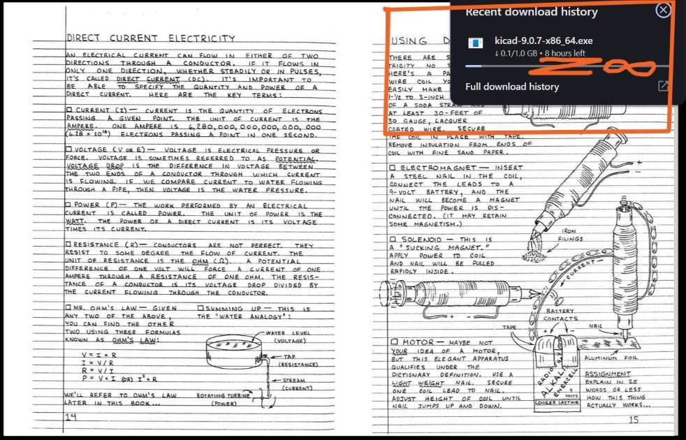
Now finished and installed fully functioning Kicad
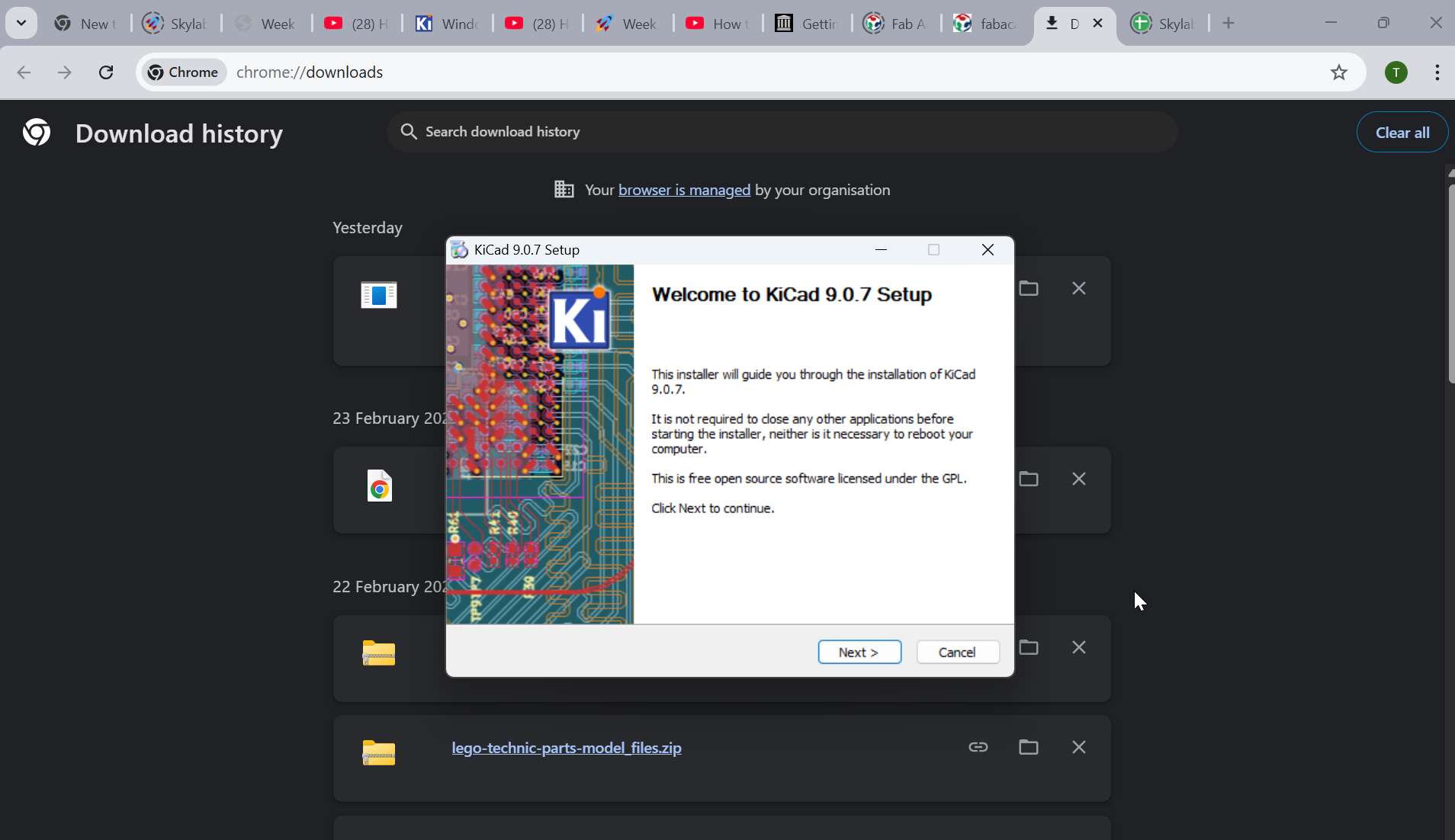
I installed Eagle too, but just kicad for now…

Done and Lets go
ESP32-C3 PCB Design Guide
KiCad 9.0 – Standard Hierarchical Workflow
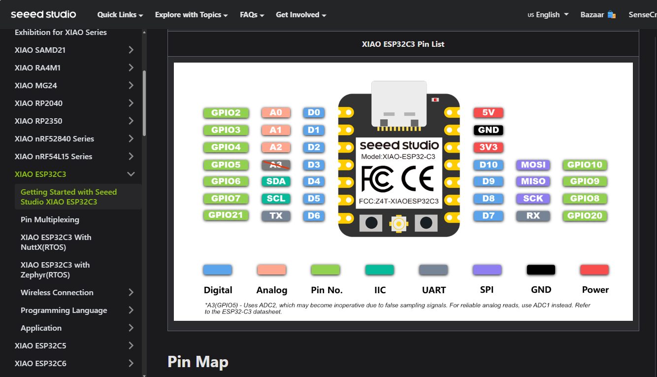
ESP32-C3 Custom Board from the datasheet to own designed one
- Data sheet is reccommeneded when ever design
Overview
This guide explains step-by-step how to I tried to design my first MCU (ESP32-C3) usind Kicad:
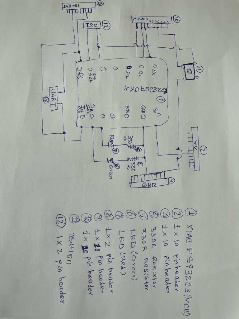
My hand sketch and basic understanding of the elecronics symbols and connection methods
- Create a custom ESP32-C3 symbol
- Design a clean schematic using hierarchy
- Assign footprints correctly
PART 1 — Creating a Custom ESP32-C3 Symbol
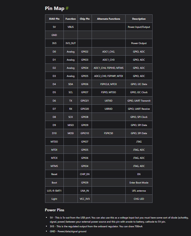
- Careful study the pin
1. Open Symbol Editor
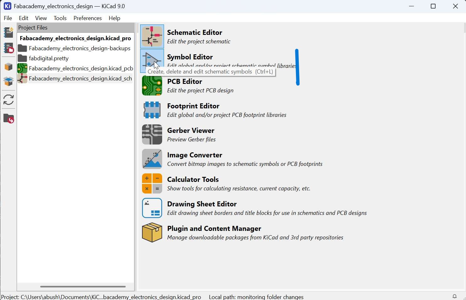
- Open KiCad 9.0
- Click Symbol Editor
2. Create a Custom Library
- File → New Library
- Choose Global Library
- Name it:
My_ESP32_Library - Save
3. Create New Symbol
- Right-click your library → New Symbol
- Name:
ESP32-C3-WROOM - Reference: U
- Value: ESP32-C3
4. Draw Symbol Body
- Use Rectangle Tool (Shift + R)
- Create a clean rectangular body
- Adjust thickness in Properties
5. Add Pins (Important Step)
Press P to add pins.
From ESP32-C3 datasheet add:
Power Pins
- 3V3 → Power Input
- GND → Power Input
- EN → Input
UART
- TXD
- RXD
GPIO (D, Tx, RX, MISO, MOSI in my case)
-D1–D10 (as required)
Electrical Types
Set correctly: - Power Input → 5V, 3V3, GND - Input → EN, Boot - Bidirectional → GPIO - Output → TX
- THIS TOOL IS USEFUL FOR PINs
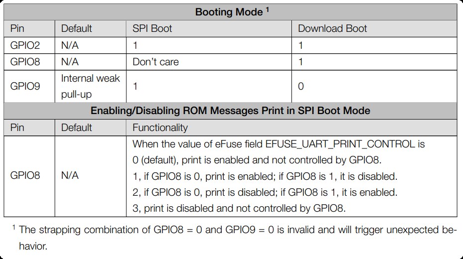
Correct pin types prevent ERC errors.
6. Organize Pins
- Left side → Inputs
- Right side → Outputs
- Bottom → Power
- Keep clean spacing
7. Save Symbol
- Save frequently
- Close Symbol Editor
PART 2 — Schematic Design
Open Schematic Editor
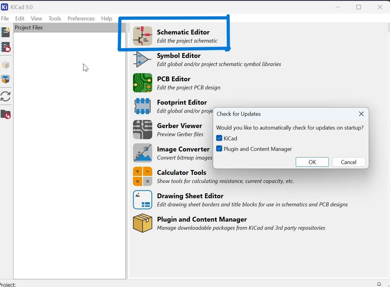
Project Structure
Footprint Assignment
Open Footprint Assignment Tool
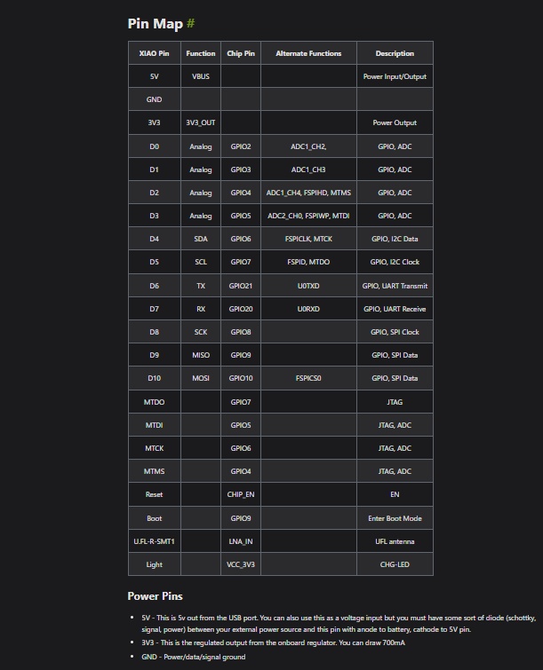
Match: Confirm pad sizes match datasheet for pins (here is the ESP32C3 MCU Pins map).
Update PCB
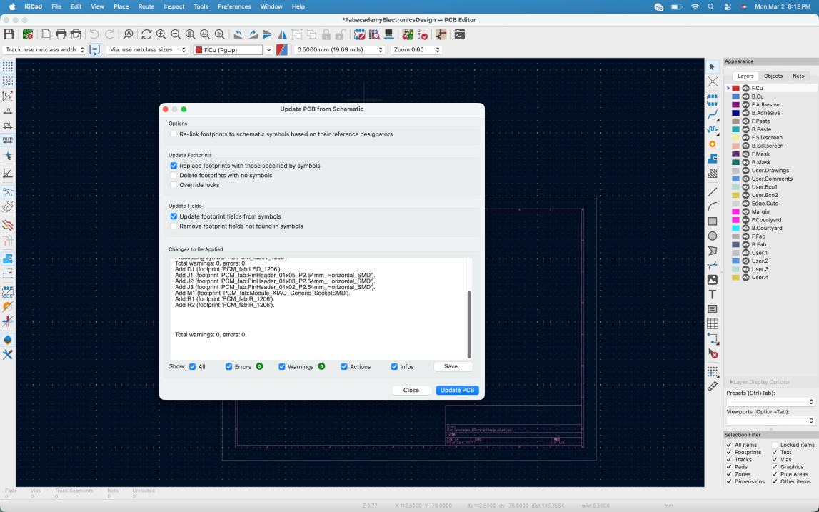
Tools → Update PCB from Schematic
Press F8
Component Placement Strategy
Follow this order:
- Place ESP32 center
- Place decoupling capacitors VERY close to VDD
- Place LDO near power input
- Place USB near board edge, if neeed
- Place buttons accessible
- Place headers at edges
- Place LEDs visible
Generally
This document covers:
- Custom symbol creation
- Clean hierarchical schematic
- Correct footprint assignment
- Professional PCB design
Final
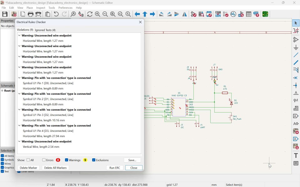
Need to debug and update on the errors
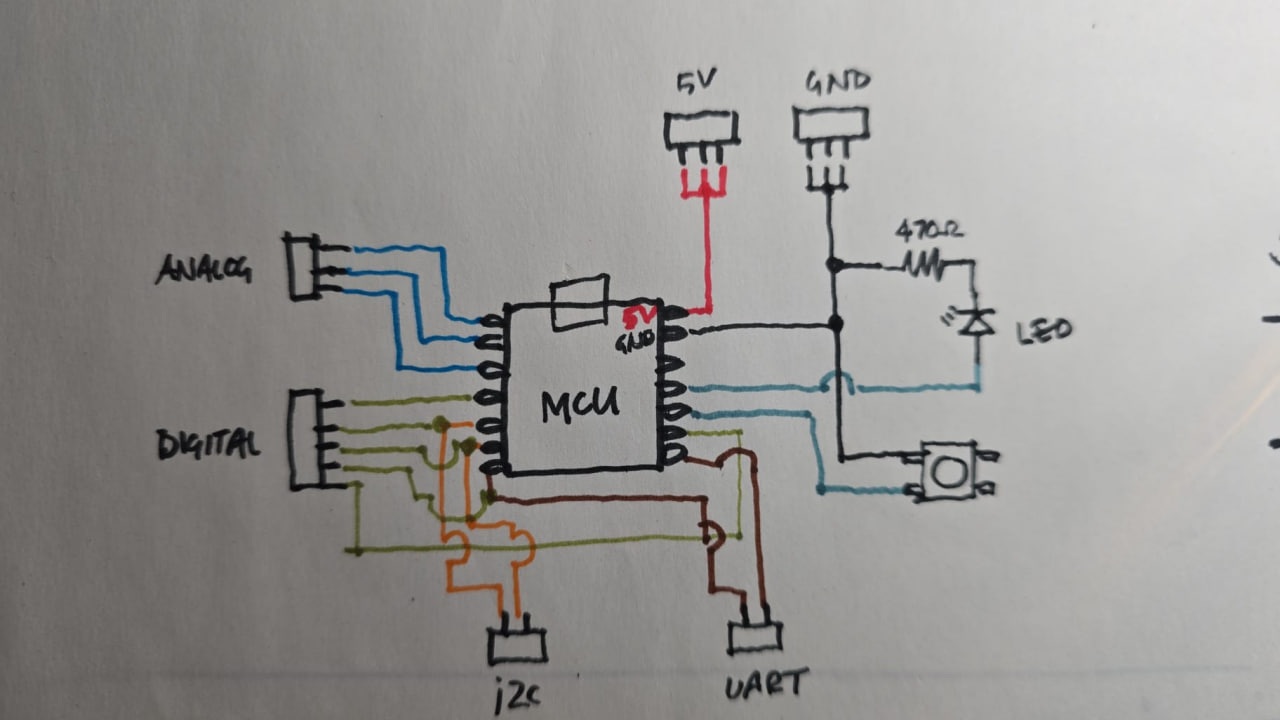
The MCU is intgrated to the component shared by Rico and the source is ,Rico(Local instructor) for the sketch bellow
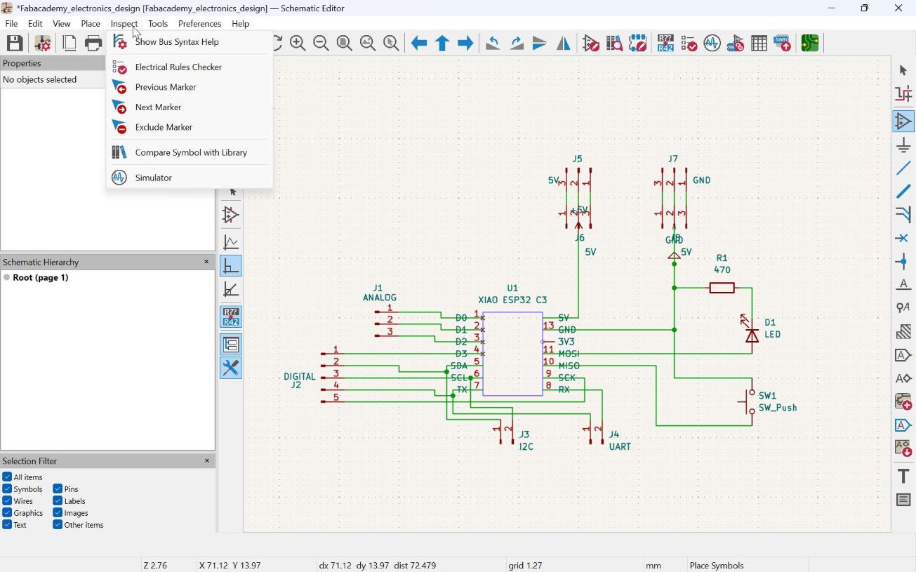
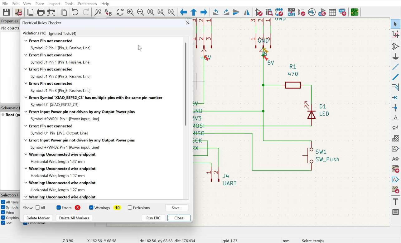
Correction and update by Rico
All the a bove was my practice and the following with great improvement is after Rico add more local session.
Define what the board must do. For my development board: power the ESP32-C3, program it, blink/debug, reset, and break out GPIO. I used Rico’s hand sketch and the Fab Academy electronics inventory as the starting circuit, not a random set of parts.
Choose parts that exist in the lab / fab library. ESP32-C3 module, resistors, capacitors, LEDs, buttons, and headers. Voltage must stay compatible (3.3 V logic).
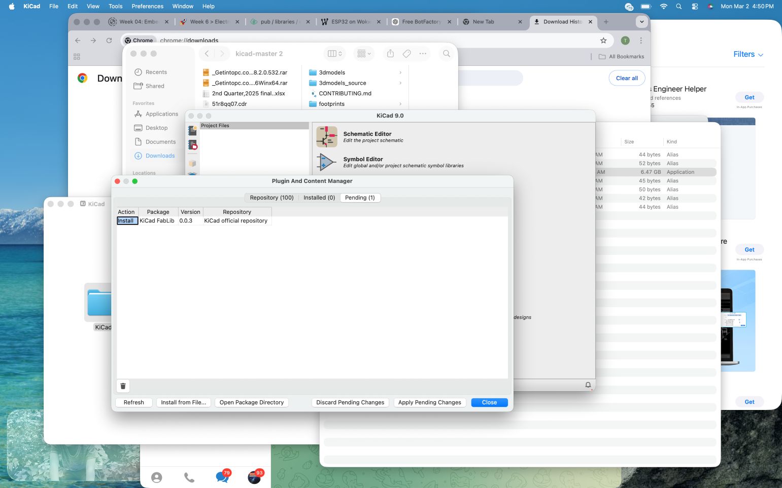
Install the Fab electronics library in KiCad so symbols and footprints match what Fab Academy actually uses.
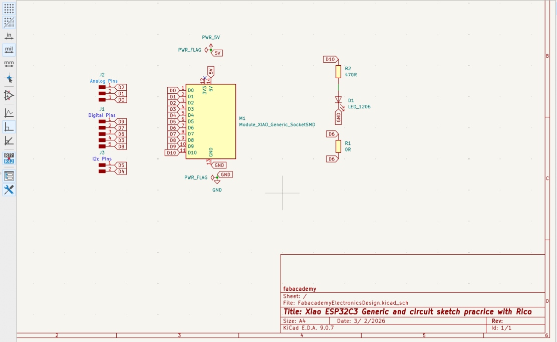
Draw the schematic in Schematic Editor: place symbols, wire nets, add power flags/ports, and label important nets (3V3, GND, TX, RX, EN). Hierarchy keeps power, MCU, and I/O readable.
Run Electrical Rules Check (ERC). ERC is KiCad telling me the drawing of the circuit is illegal or incomplete (pin types, missing power, unconnected pins). I opened Inspect → Electrical Rules Checker, ran it, and fixed errors before trusting the schematic. The earlier practice schematic had eight ERC errors; after Rico’s session I rechecked until the important errors were gone.
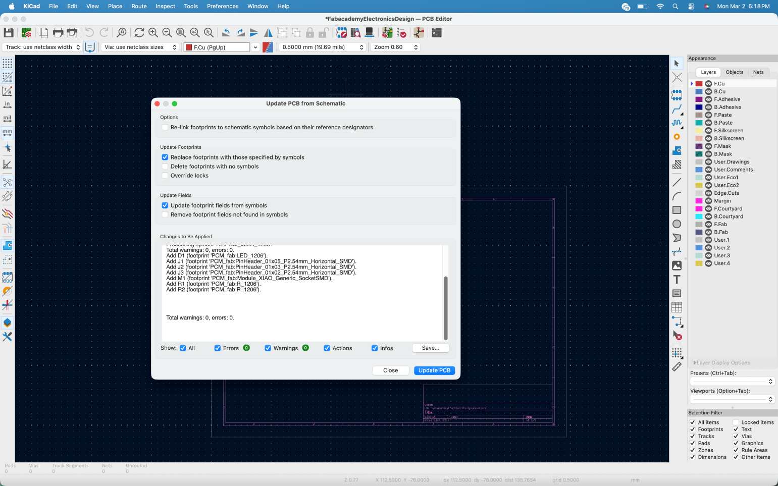
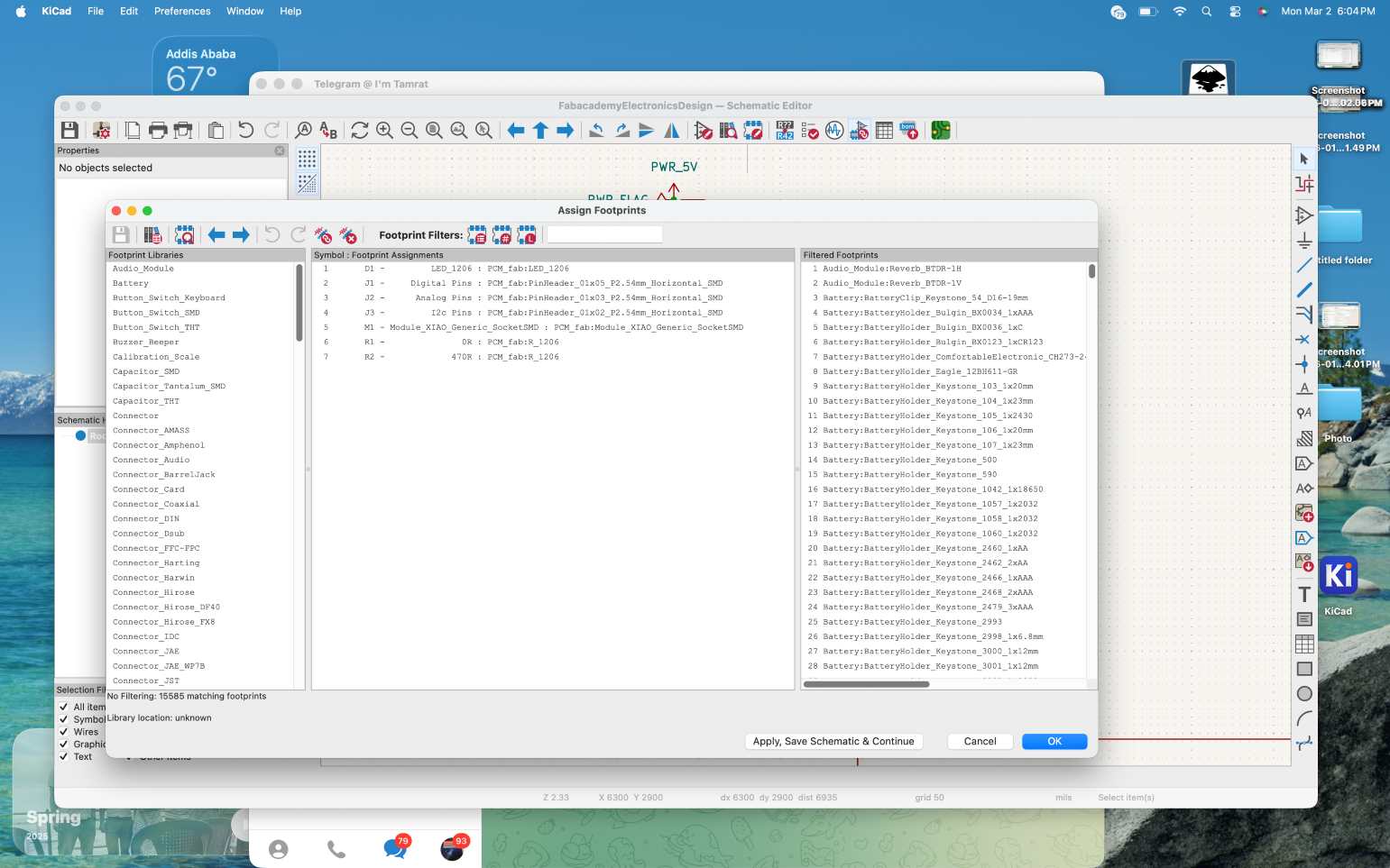
Assign footprints (what this image is, and why I did it).
A schematic symbol is only a logical drawing. A footprint is the real copper pads and outline that will be milled or fabricated. After ERC, I opened Tools → Assign Footprints (footprint assignment tool). For each symbol I picked the matching Fab library footprint (ESP32-C3 module, 0805/1206 passives, LED, button, header).
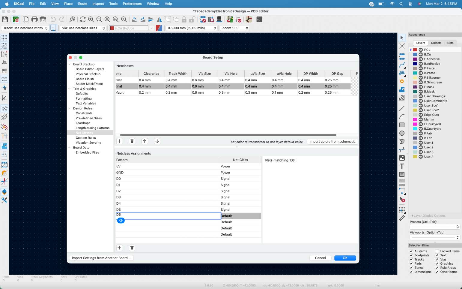
Set Design Rules / Net Classes
Board Setup → Design Rules → Net Classes is where I tell KiCad the copper rules for this machine, not for a random factory. For our mill I used the class constraints from class: minimum trace width 0.4 mm and minimum clearance 0.4 mm.
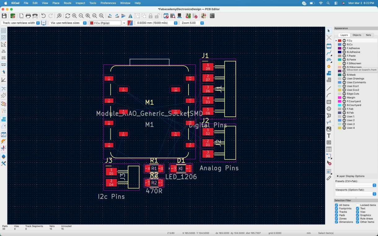
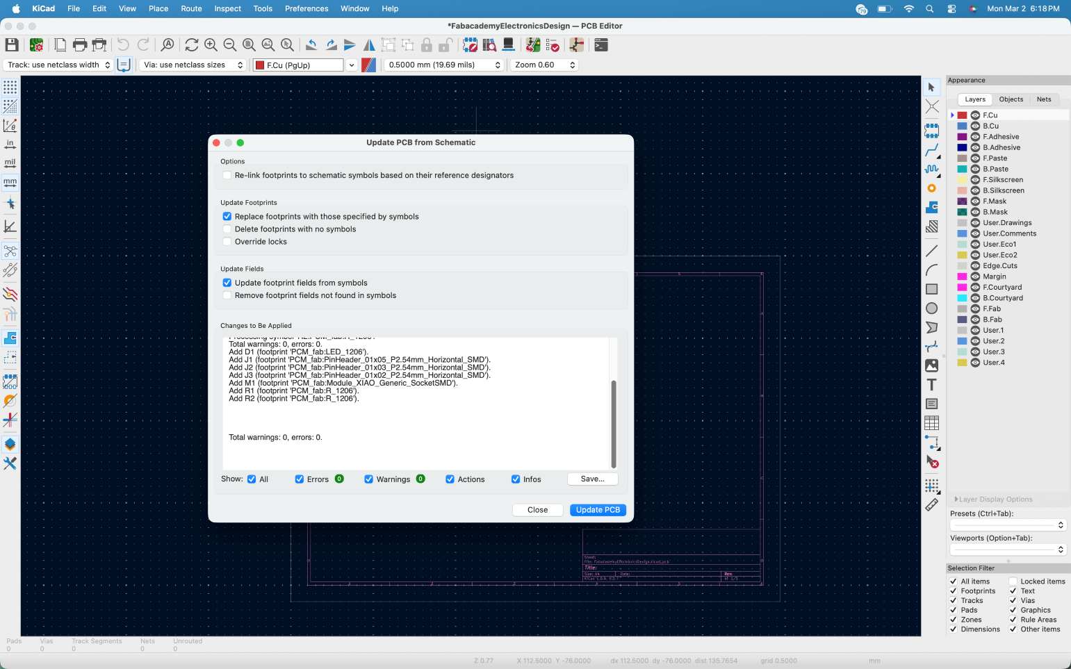
Push the schematic into the PCB editor (F8).
Tools → Update PCB from Schematic (F8) copies footprints and ratsnest (airwires) onto the board. I used F8 whenever the schematic changed so the PCB would not stay on an old netlist.
Create the board outline.
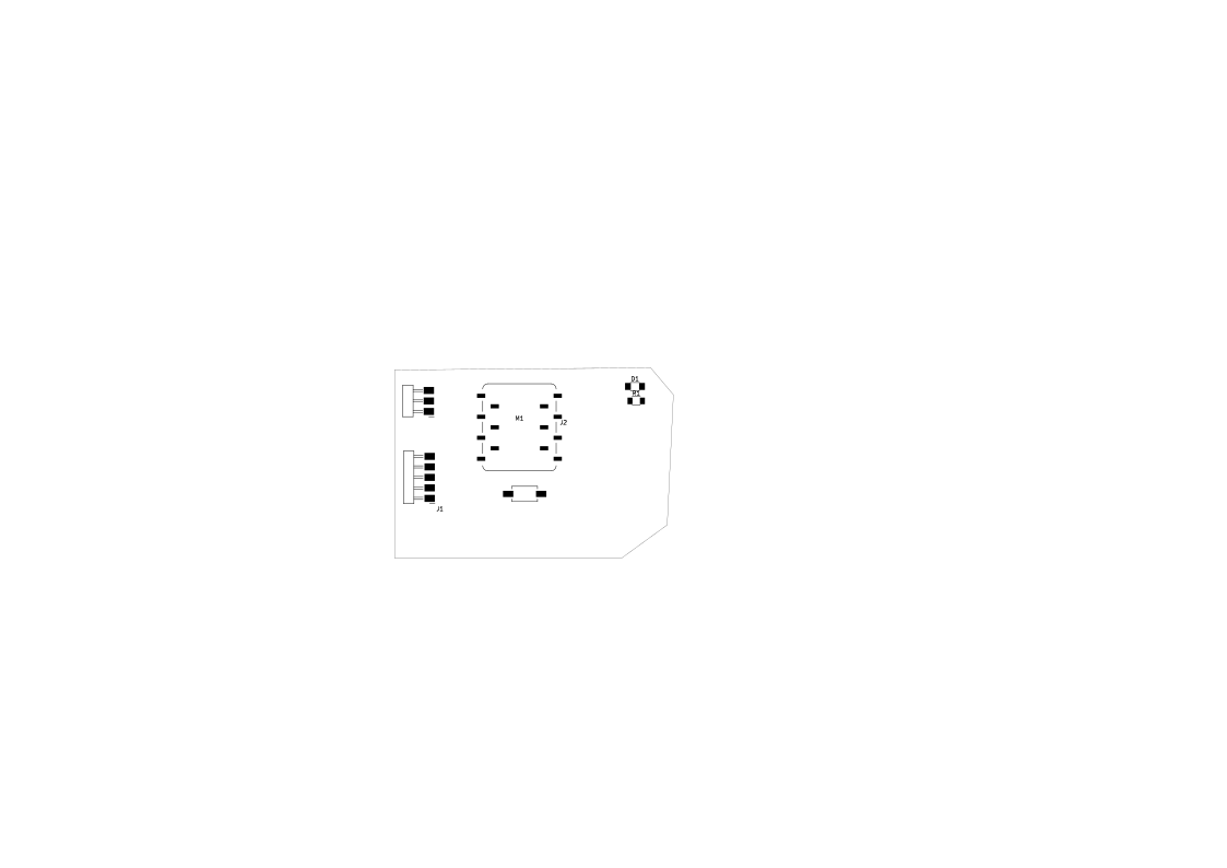
In the PCB editor I selected the Edge.Cuts layer. That layer is not copper — it is the cut path of the board. I chose Place → Rectangle (or graphic lines) and drew a rectangle around the placed parts, leaving extra margin so headers, USB if used, and the mill cutter have room.
Place components on the board.
I followed the placement order from class: ESP32-C3 near the center, decoupling capacitors as close as possible to VDD/3V3 pins, power input / regulator near the edge, buttons where a finger can reach them, headers on the outline, LEDs visible.
I rotated parts so traces would be short.
Draw the trace lines (pad-to-pad connections).
After placement, KiCad shows thin ratsnest lines: these are not copper yet, only “this pad must connect to that pad.” To make real connections I switched to the copper layer (F.Cu for the front). I used Route → Route Single Track (or the track toolbar button). Method I used for each net:
- Click the starting pad.
- Move the cursor; the track follows the grid.
- Click to put a corner if I need to go around another pad.
- Click the destination pad on the same net until the ratsnest for that connection disappears.
- Keep traces on the 0.4 mm width from Net Classes; if KiCad refused a path, clearance was too small and I moved a part or went around.
I avoided sharp 90° corners where I could, kept the 3V3/GND paths short, and did not let a signal trace squeeze between pads closer than 0.4 mm.
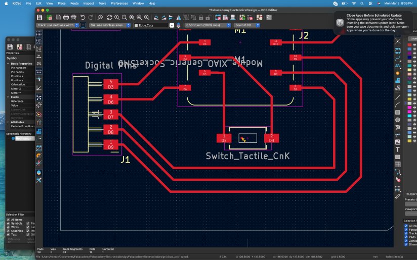
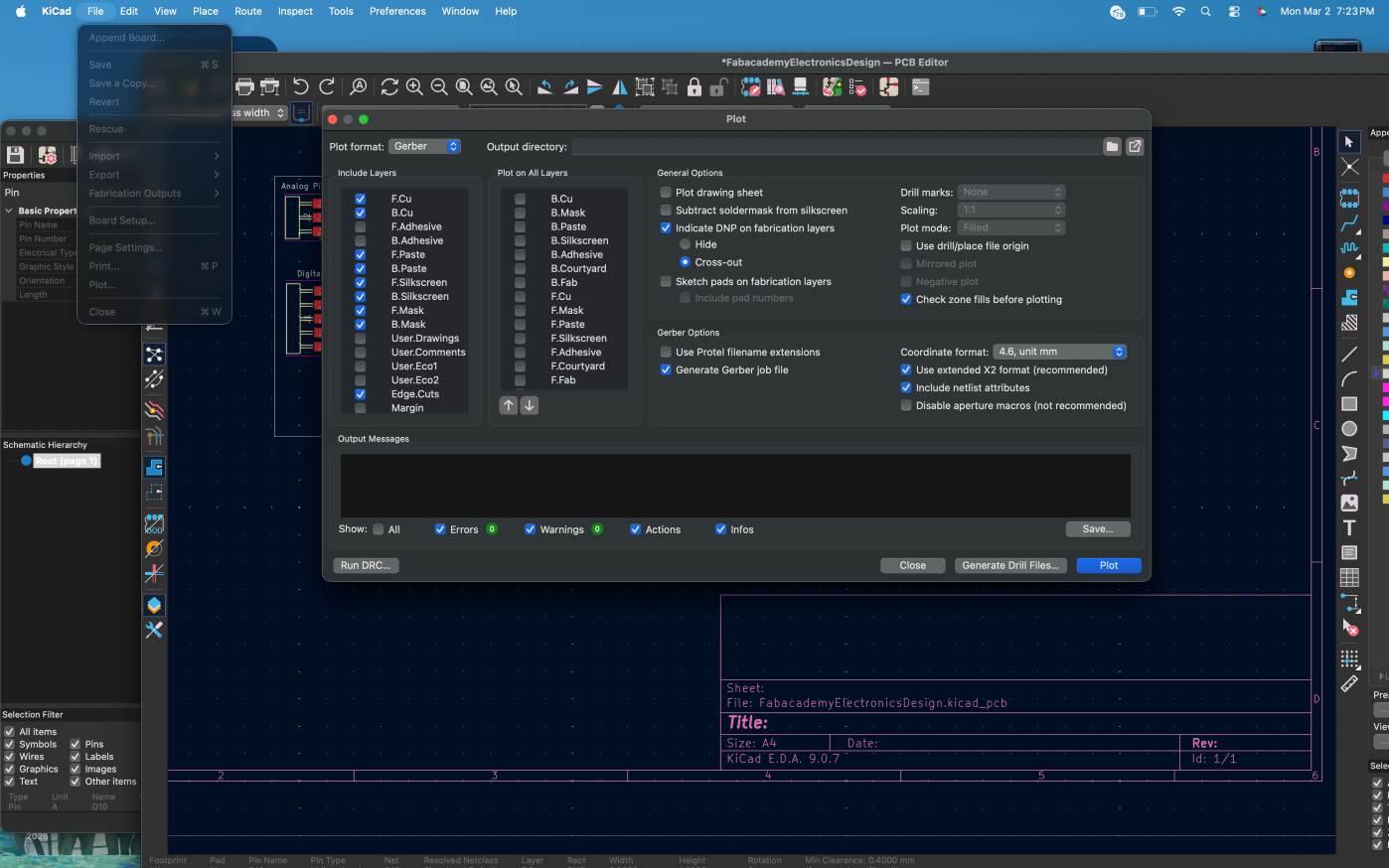
Save in the formats needed (KiCad project, and export for the next machine step).
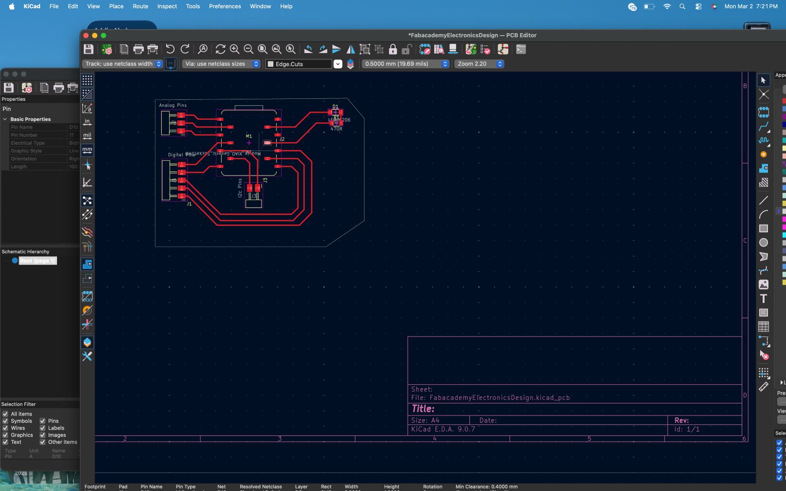
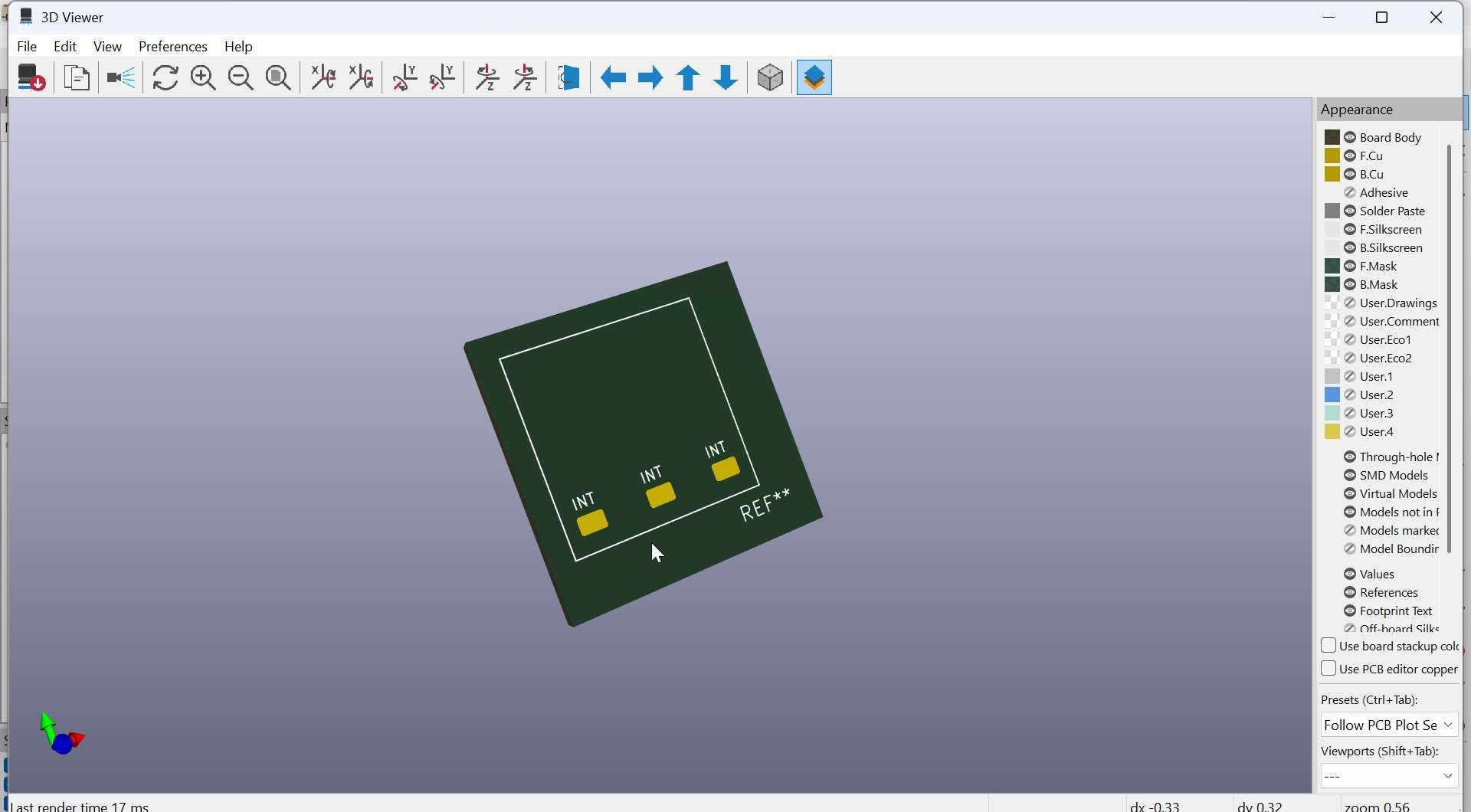
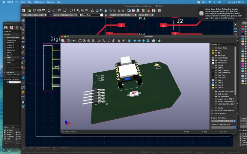
Check in 3D (Ctrl+Shift+F3) to see if the outline, module, and headers look physically possible before milling or PNP.
Prepare for cut / print / PNP. In my case I looked at a printer such as BotFactory SV2, so paste and ink for pick-and-place (PNP) is more considered than only cut and drills.
Simulation (Wokwi)
ESP32 – 3 Lane Traffic Light (T-junction)
Objective
Simulate a 3-lane traffic light system using an ESP32 in Wokwi. code is generated from ChatGPT with promt “give bsic code for trafic light with three lanes”.
Learning and understanding from this:
- GPIO (Genral Purpose input/output) configuration on ESP32
- Digital output control
- Sequential timing logic
- Wokwi simulation workflow
- Safe LED interfacing with microcontrollers
Each lane has: - Red - Yellow - Green
Only one lane is green at a time. Board used in simulation: ESP32 Dev Module (Wokwi default based on ESP32)
Platform
Simulation is done using: - Wokwi Online Simulator (https://wokwi.com) , might be needed to create account/free - ESP32 (Arduino framework compatible)
Step 1: Create Project
- Go to https://wokwi.com
- Click New Project
- Select ESP32
- Rename project to:
ESP32_3_Lane_Traffic_Light
Step 2: Add Components
Add the following components from the Wokwi parts menu:
- 1 × ESP32
- 9 × LEDs
- 3 Red
- 3 Yellow
- 3 Green
- 9 × Resistors (220Ω recommended)
Step 3: Wiring Connections
Standard LED Connection Rule
GPIO → 220Ω Resistor → LED (Anode / Long Leg)
LED (Cathode / Short Leg) → GND
Each LED must have its own resistor.
All LED cathodes connect to GND.
Lane 1 Connections
| Color | GPIO |
|---|---|
| Red | 23 |
| Yellow | 22 |
| Green | 21 |
Lane 2 Connections
| Color | GPIO |
|---|---|
| Red | 19 |
| Yellow | 18 |
| Green | 5 |
Lane 3 Connections
| Color | GPIO |
|---|---|
| Red | 17 |
| Yellow | 16 |
| Green | 4 |
Pin Summary Table
| Lane | Red | Yellow | Green |
|---|---|---|---|
| Lane 1 | 23 | 22 | 21 |
| Lane 2 | 19 | 18 | 5 |
| Lane 3 | 17 | 16 | 4 |
Step 4: Code (sketch.ino)
Code Generated with AI (chatGPT) prompt “Generate the yellow,red and green traffic light controlling codes”
Then understand each code line by line and Replace the default code with:
// Lane 1
#define L1_RED 23
#define L1_YELLOW 22
#define L1_GREEN 21

// Lane 2
#define L2_RED 19
#define L2_YELLOW 18
#define L2_GREEN 5

// Lane 3
#define L3_RED 17
#define L3_YELLOW 16
#define L3_GREEN 4

const int GREEN_TIME = 5000;
const int YELLOW_TIME = 2000;

void setup() {

  pinMode(L1_RED, OUTPUT);
  pinMode(L1_YELLOW, OUTPUT);
  pinMode(L1_GREEN, OUTPUT);

  pinMode(L2_RED, OUTPUT);
  pinMode(L2_YELLOW, OUTPUT);
  pinMode(L2_GREEN, OUTPUT);

  pinMode(L3_RED, OUTPUT);
  pinMode(L3_YELLOW, OUTPUT);
  pinMode(L3_GREEN, OUTPUT);

  allRed();
}

void loop() {
  lane1();
  lane2();
  lane3();
}

void allRed() {
  digitalWrite(L1_RED, HIGH);
  digitalWrite(L2_RED, HIGH);
  digitalWrite(L3_RED, HIGH);

  digitalWrite(L1_YELLOW, LOW);
  digitalWrite(L2_YELLOW, LOW);
  digitalWrite(L3_YELLOW, LOW);

  digitalWrite(L1_GREEN, LOW);
  digitalWrite(L2_GREEN, LOW);
  digitalWrite(L3_GREEN, LOW);
}

void lane1() {
  allRed();
  digitalWrite(L1_RED, LOW);
  digitalWrite(L1_GREEN, HIGH);
  delay(GREEN_TIME);

  digitalWrite(L1_GREEN, LOW);
  digitalWrite(L1_YELLOW, HIGH);
  delay(YELLOW_TIME);

  digitalWrite(L1_YELLOW, LOW);
  digitalWrite(L1_RED, HIGH);
}

void lane2() {
  allRed();
  digitalWrite(L2_RED, LOW);
  digitalWrite(L2_GREEN, HIGH);
  delay(GREEN_TIME);

  digitalWrite(L2_GREEN, LOW);
  digitalWrite(L2_YELLOW, HIGH);
  delay(YELLOW_TIME);

  digitalWrite(L2_YELLOW, LOW);
  digitalWrite(L2_RED, HIGH);
}

void lane3() {
  allRed();
  digitalWrite(L3_RED, LOW);
  digitalWrite(L3_GREEN, HIGH);
  delay(GREEN_TIME);

  digitalWrite(L3_GREEN, LOW);
  digitalWrite(L3_YELLOW, HIGH);
  delay(YELLOW_TIME);

  digitalWrite(L3_YELLOW, LOW);
  digitalWrite(L3_RED, HIGH);
}
Wokwi Simulation practice with 3 lane trafic light
Step 5: Run Simulation
Click Start Simulation
Observe the traffic sequence:
- Lane 1 → Green → Yellow → Red
- Lane 2 → Green → Yellow → Red
- Lane 3 → Green → Yellow → Red
The cycle repeats continuously.
System Logic Explanation
- At startup, all lanes are set to RED
- Each lane turns GREEN for 5 seconds
- Then YELLOW for 2 seconds
- Then back to RED
- Only one lane is GREEN at any time
Electrical Notes
- Use 220Ω or 330Ω resistors
- ESP32 operates at 3.3V logic level
- Do NOT connect LEDs directly without a resistor
- Ensure correct LED polarity (long leg = Anode +)
- Use rename or recoloring of the componnent whenever needed