Week 8 Electronics Production
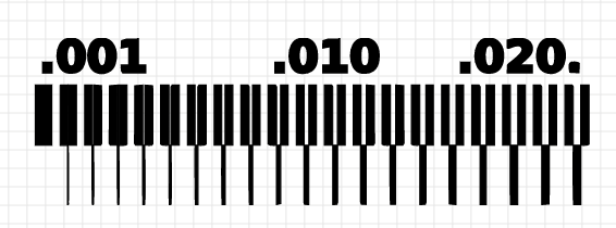
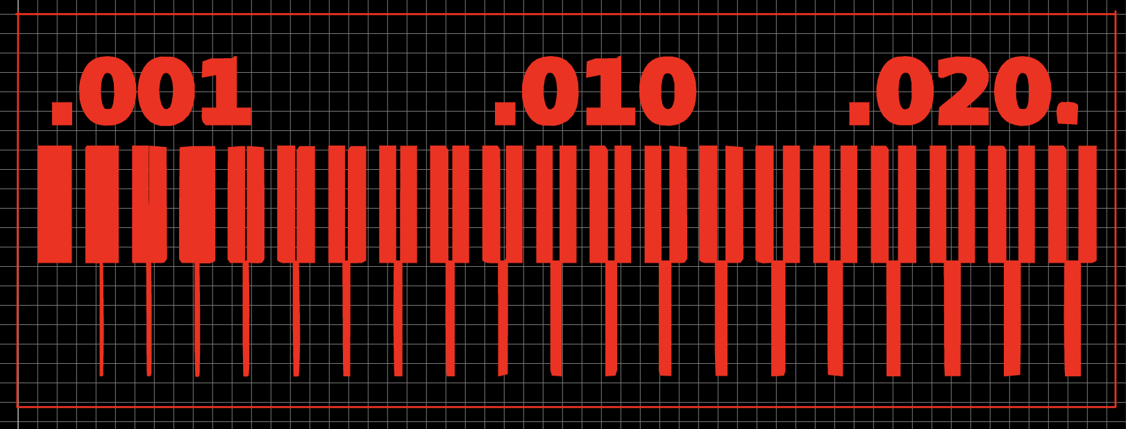
1 — Understanding PCB Milling Width Test Pattern
The electronics production process started with understanding how thin traces can be reliably milled using the PCB milling machine. A trace-width test pattern was selected containing different line spacings such as .001, .010, and .020. These values represent the spacing and trace width in inches. The purpose of this test was to identify the minimum width the milling machine could cut without damaging nearby copper traces. This is an important step because PCB milling accuracy directly depends on tool diameter, spindle stability, and machine calibration. Before milling an actual circuit board, testing these values helps avoid broken traces or electrical short circuits.
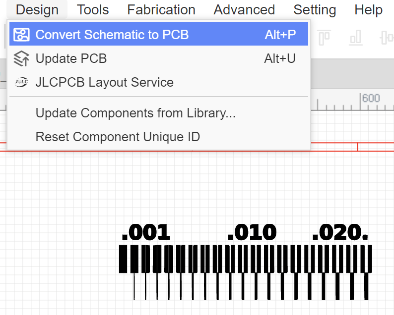
2 — Importing the Design into EasyEDA PCB Workspace
The PCB design workflow was initiated in EasyEDA by converting the schematic into a PCB layout. The “Convert Schematic to PCB” option automatically transferred the electronic connections and component footprints into the PCB editor. This process creates the physical board layout from the logical circuit diagram. At this stage, the PCB workspace becomes the area where traces, copper layers, and component positions are prepared for fabrication. Understanding this conversion step is essential because PCB manufacturing requires physical geometry rather than schematic symbols.
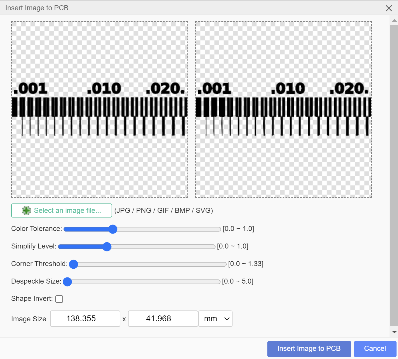
3 — Inserting the Trace Test Image into PCB Layout
The trace-width test image was imported into the PCB design environment using the “Insert Image to PCB” feature. During this step, parameters such as color tolerance, simplify level, corner threshold, and despeckle size were adjusted to properly convert the image into vector geometry. These settings affect how accurately the software interprets the image edges and converts them into PCB copper regions. The imported image was also scaled according to the required physical dimensions. This allowed the design to become compatible with PCB manufacturing and Gerber export.
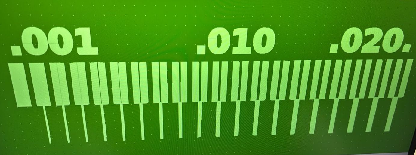
4 — Generated PCB Trace Geometry
After processing the imported image, the software generated the final PCB trace geometry shown in red. This preview represents the actual copper traces that would remain after milling. At this stage, the spacing between the traces becomes critical because the milling bit physically removes copper between adjacent paths. The preview helped verify whether the thinner traces were manufacturable using the available engraving tool. This step acts as a visual inspection stage before exporting manufacturing files.
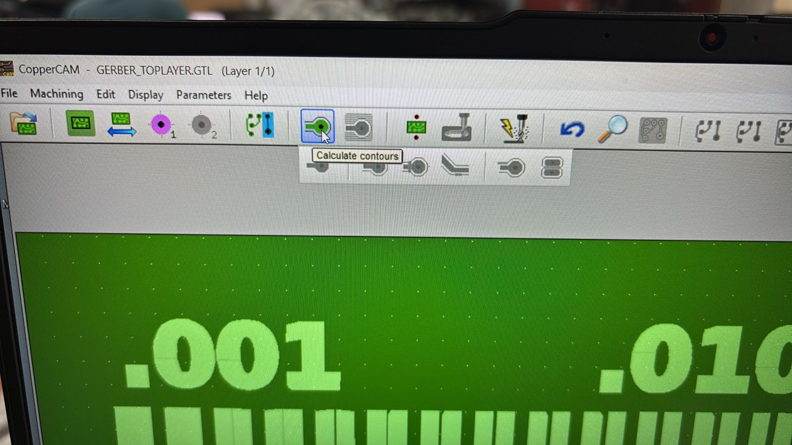
5 — Gerber File Verification in CopperCAM
The exported Gerber file was opened in CopperCAM for toolpath generation and machining preparation. CopperCAM is a CAM software commonly used for PCB milling operations. The imported PCB geometry was displayed in green, representing the copper layer that would remain on the board. Before generating toolpaths, the design was carefully inspected to ensure that all traces, spacing, and text details were imported correctly. Verifying the Gerber file at this stage helps prevent machining errors during PCB fabrication.
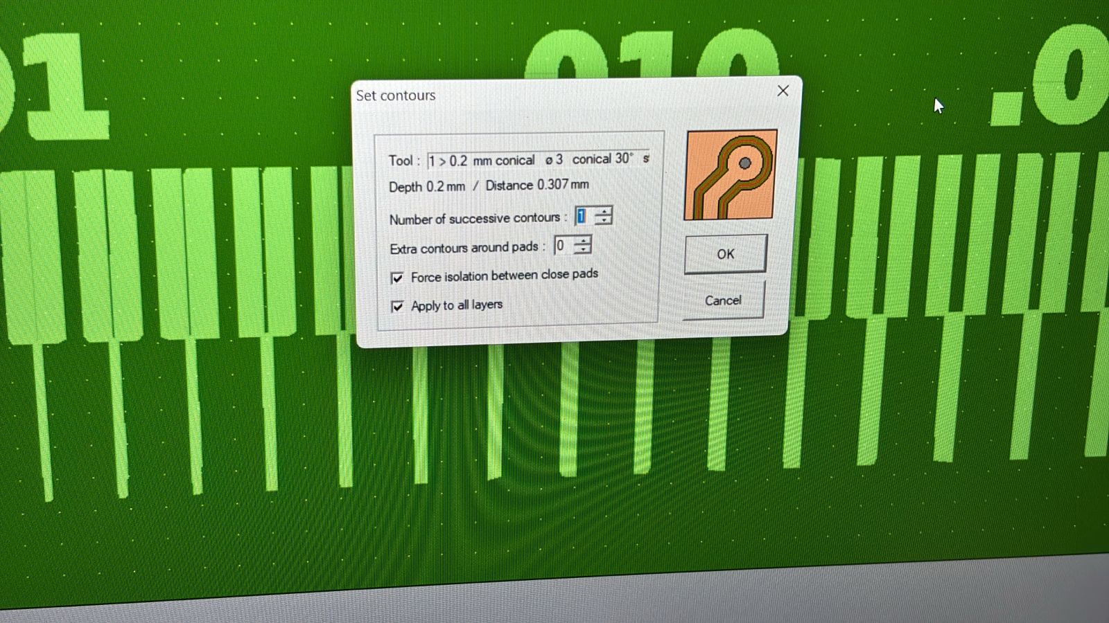
6 — Calculating Isolation Contours for PCB Milling
The “Calculate Contours” operation was used to generate isolation paths around the PCB traces. In PCB milling, the machine removes copper around the traces instead of chemically etching the board. Isolation contours define the exact regions where the milling bit will cut. This process is extremely important because insufficient contour spacing can cause electrical shorts between traces. The generated contours also depend on the diameter and angle of the engraving bit being used.
7 — Configuring PCB Milling Parameters
The contour settings were configured according to the engraving tool specifications. A conical engraving bit with a very fine tip diameter was selected for precise trace isolation. Parameters such as cutting depth, contour distance, and number of successive contours were adjusted to achieve cleaner trace separation. The “Force isolation between close pads” option was enabled to ensure copper removal even in narrow regions. These settings directly influence the final PCB quality and determine whether fine traces can be milled successfully.
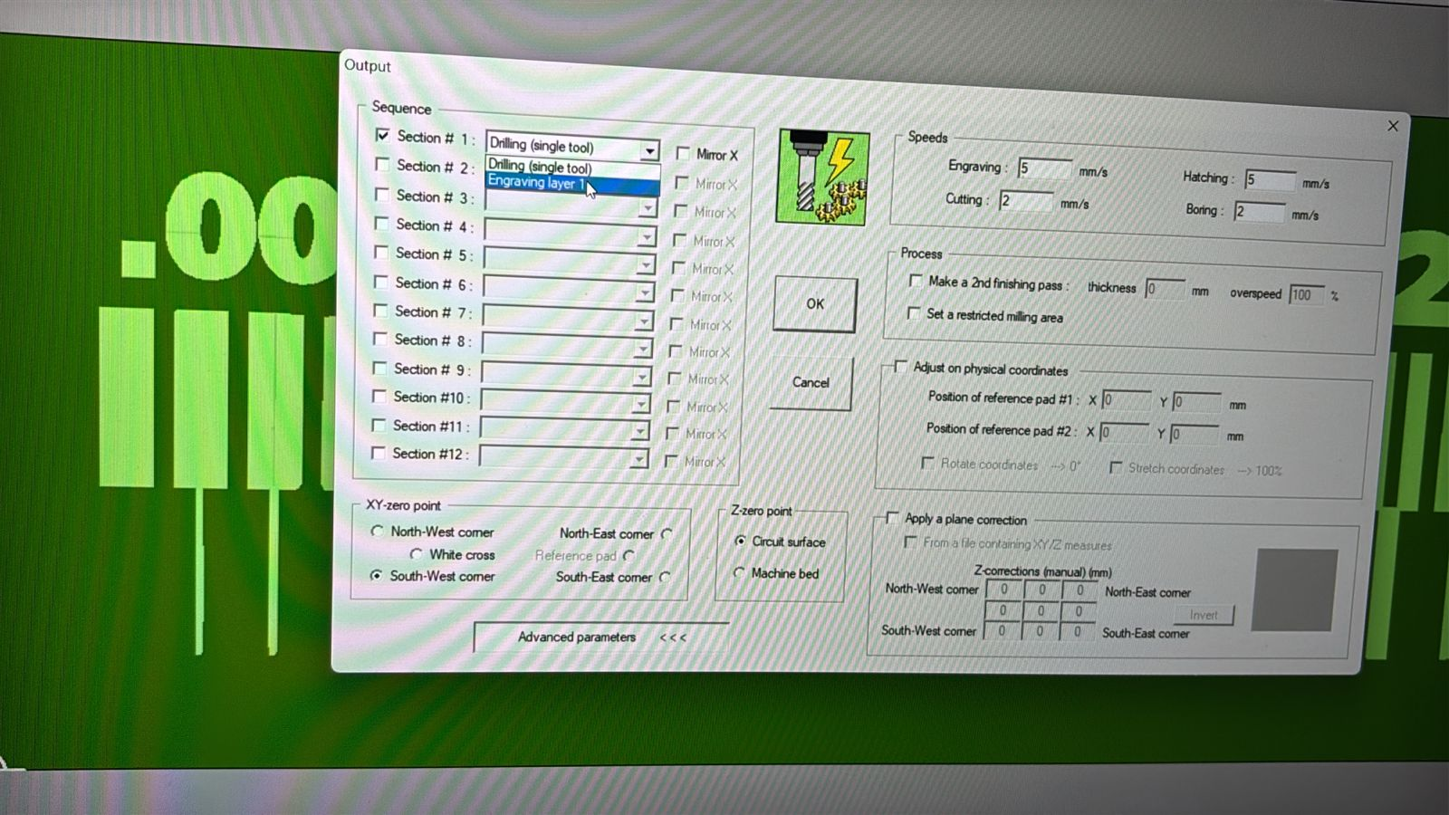
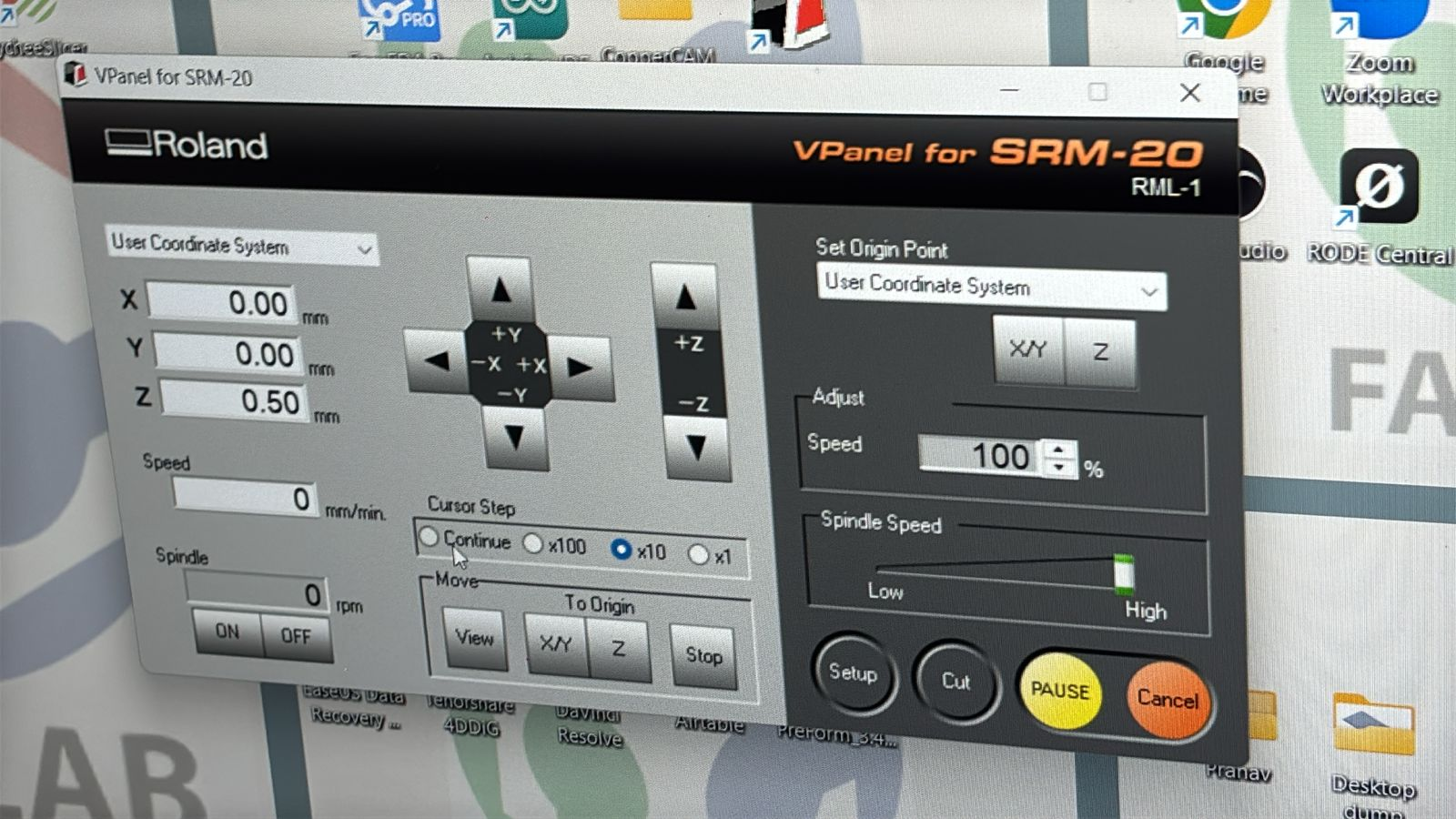
8 — Preparing Final Output Settings for SRM-20
The final machining output settings were configured before generating the milling file for the Roland SRM-20 PCB milling machine. Different machining operations such as drilling and engraving were organized into separate sections. Feed rates for engraving and cutting were adjusted according to the material and tool size. The XY zero point and Z reference point were also defined so the machine could accurately determine the starting position on the PCB board. Proper setup of these parameters is necessary to avoid tool crashes and incorrect milling depth.
9 — Preparing the FR1 Copper-Clad Board
A small FR1 copper-clad board was prepared for mounting onto the milling bed. Double-sided adhesive tape was attached to the back of the board to hold it firmly in place during machining. FR1 material is commonly used for PCB milling because it is easier to machine compared to fiberglass-based FR4 boards. Properly fixing the board is important because even slight movement during milling can damage fine traces and reduce dimensional accuracy.
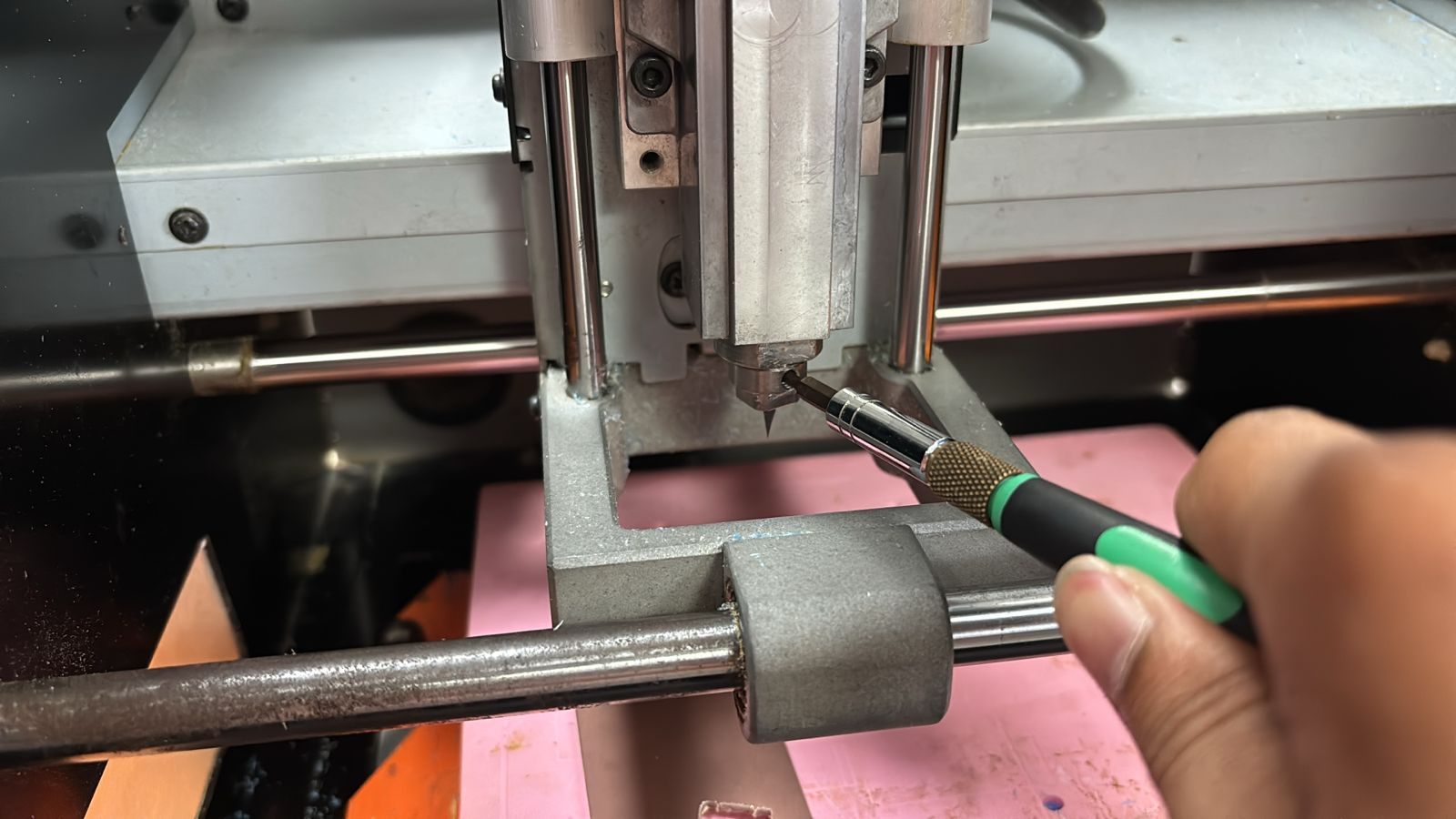
10 — Installing the Engraving Bit into the SRM-20
The engraving bit was carefully installed into the spindle of the Roland SRM-20 milling machine using a precision tightening tool. The engraving bit used for PCB isolation is extremely fragile due to its sharp conical tip. During installation, the bit must be handled carefully to avoid breakage or misalignment. Correct tool installation ensures stable spindle rotation and accurate milling performance. This stage prepared the machine for the actual PCB engraving operation.
11 — Setting the Z-Axis Reference Height
The Z-axis height was manually calibrated by lowering the engraving bit close to the PCB surface. The bit was gently released until it lightly touched the copper surface before tightening it again. This process establishes the exact zero reference point for the machine. Accurate Z calibration is critical in PCB milling because even a small error in height can either fail to remove copper or cut too deeply into the board substrate.
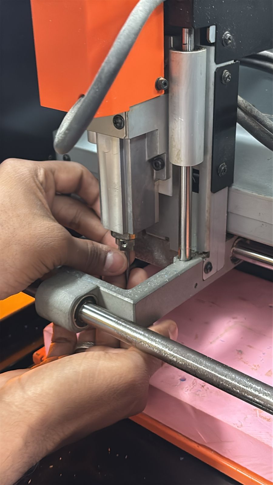
12 — Final Tool Position Verification Before Milling
Before starting the machining process, the final tool position and spindle alignment were verified manually. The engraving bit position was checked relative to the PCB surface and machine axes to ensure proper contact and clearance. This verification step helps confirm that the machine is correctly prepared for precise PCB isolation milling. Once this setup is complete, the SRM-20 becomes ready to begin engraving the copper traces onto the PCB board.
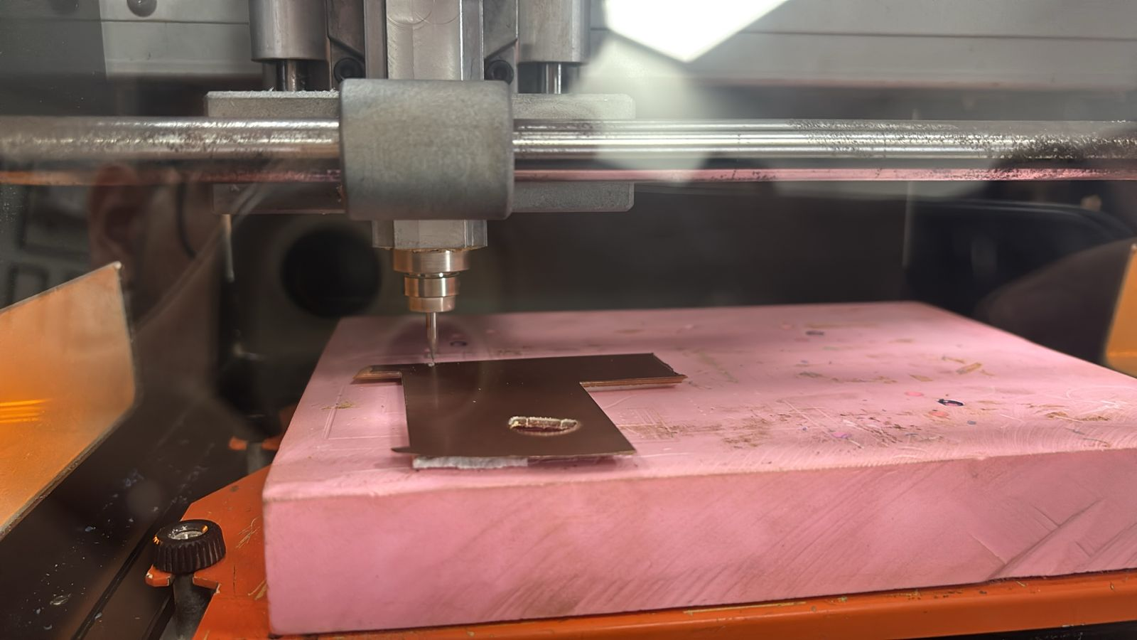
13 — Starting the PCB Engraving Process on the SRM-20
After completing all software preparation and machine setup, the PCB engraving process was initiated on the Roland SRM-20 desktop milling machine. The FR1 copper-clad board was mounted securely on the sacrificial layer using double-sided tape to prevent movement during machining. The spindle containing the engraving bit moved precisely across the copper surface to begin isolating the traces. During this process, the machine removes only a thin layer of copper around the designed paths while keeping the required conductive traces intact. This stage marked the transition from digital PCB preparation into physical PCB fabrication.
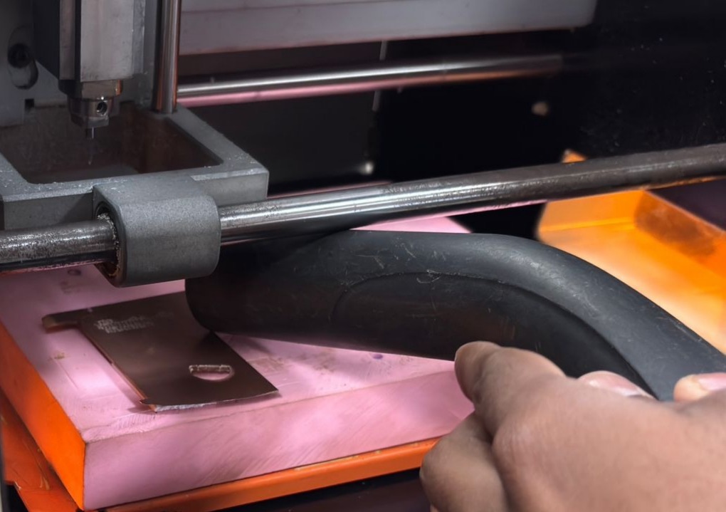
14 — Cleaning Copper Dust During Milling
As the engraving operation progressed, fine copper and substrate dust accumulated around the milled regions. A vacuum cleaner was used carefully during machining to remove this debris from the board surface. Cleaning the dust is important because excessive particles can obstruct visibility, interfere with accurate cutting, and sometimes get trapped within narrow isolation gaps. Maintaining a clean machining surface also helps in inspecting whether the engraving depth and trace separation are being produced correctly in real time.
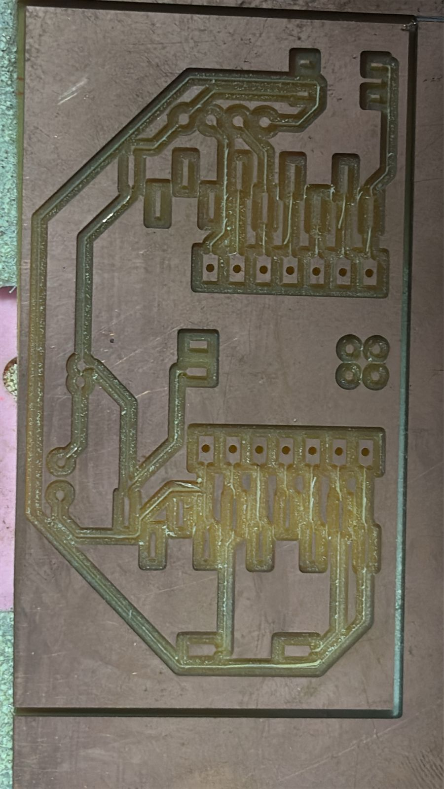
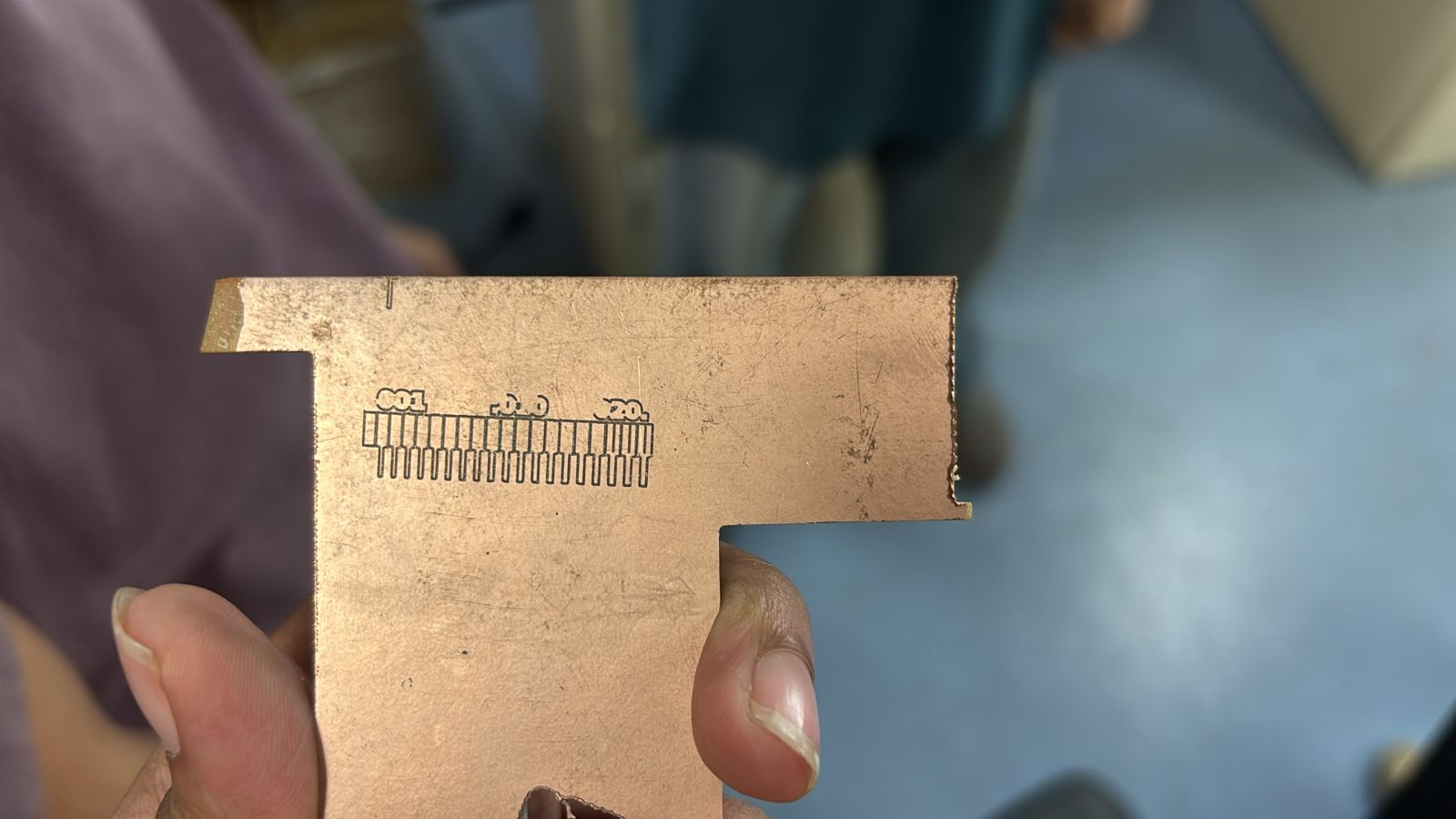
15 — Inspecting the Trace Width Test Result
After completing the milling operation, the fabricated trace-width test pattern was inspected manually. The engraved board clearly showed the isolated traces corresponding to different widths such as .001, .010, and .020. This inspection helped evaluate the practical milling capability of the engraving bit and the SRM-20 machine. Extremely thin traces appeared more delicate, while wider traces were milled more consistently. This testing stage provided a better understanding of the machine’s limitations and helped determine safer trace widths for future PCB designs.
16 — Importing the Actual PCB Design into CopperCAM
Once the trace-width testing was completed, the actual PCB circuit design was imported into CopperCAM. The PCB traces, pads, and routing paths became visible within the CAM environment. CopperCAM was used to convert the PCB design into machining toolpaths compatible with the SRM-20 milling machine. At this stage, the complete electronic routing geometry could be reviewed before generating the engraving and cutting operations. This verification ensured that all electrical connections and copper regions were correctly interpreted from the Gerber files.
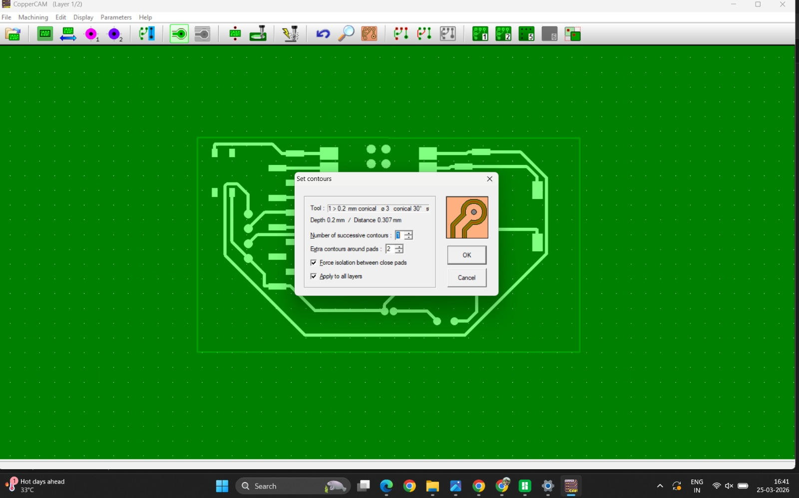
17 — Configuring Isolation Contours for the Main PCB
The contour calculation settings were configured for the final PCB design. The engraving tool selected was a fine conical engraving bit capable of isolating narrow PCB traces. Parameters such as engraving depth, contour spacing, and additional contours around pads were adjusted carefully to achieve clean copper isolation. The “Force isolation between close pads” option was enabled to ensure proper electrical separation in tightly spaced regions. These settings directly influenced the quality and readability of the final PCB traces.
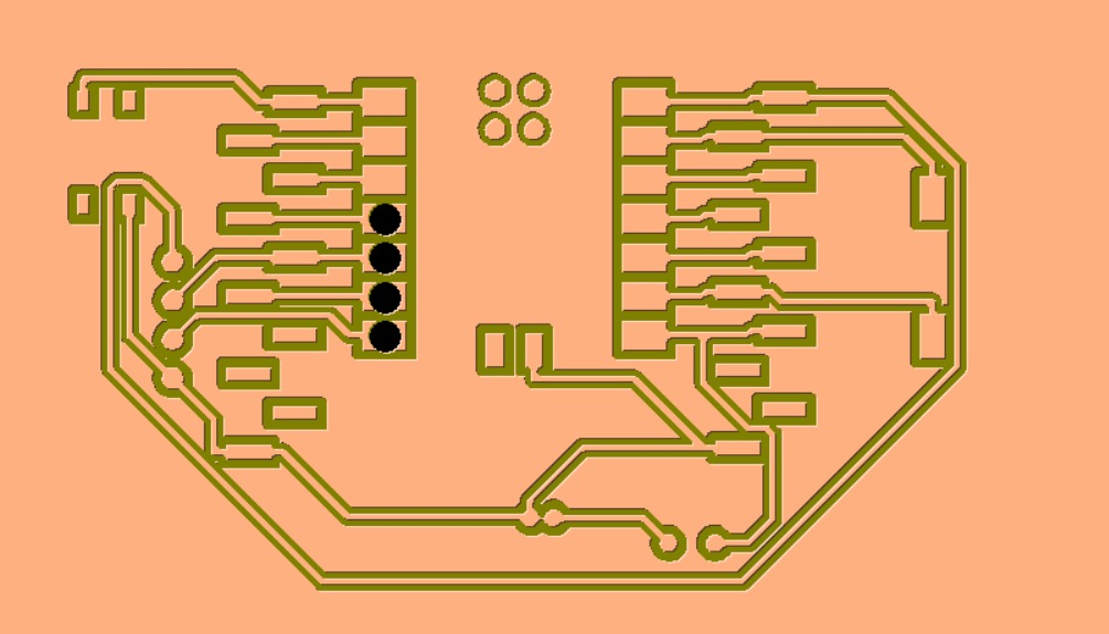
18 — Generated Isolation Toolpaths for PCB Traces
After applying the contour settings, CopperCAM generated the final isolation toolpaths around the PCB traces. The highlighted contour lines represented the exact movement path that the engraving bit would follow during milling. These paths define the regions where copper would be removed from the FR1 board. By visualizing these contours before machining, potential short circuits or insufficient spacing issues could be identified and corrected early in the workflow.
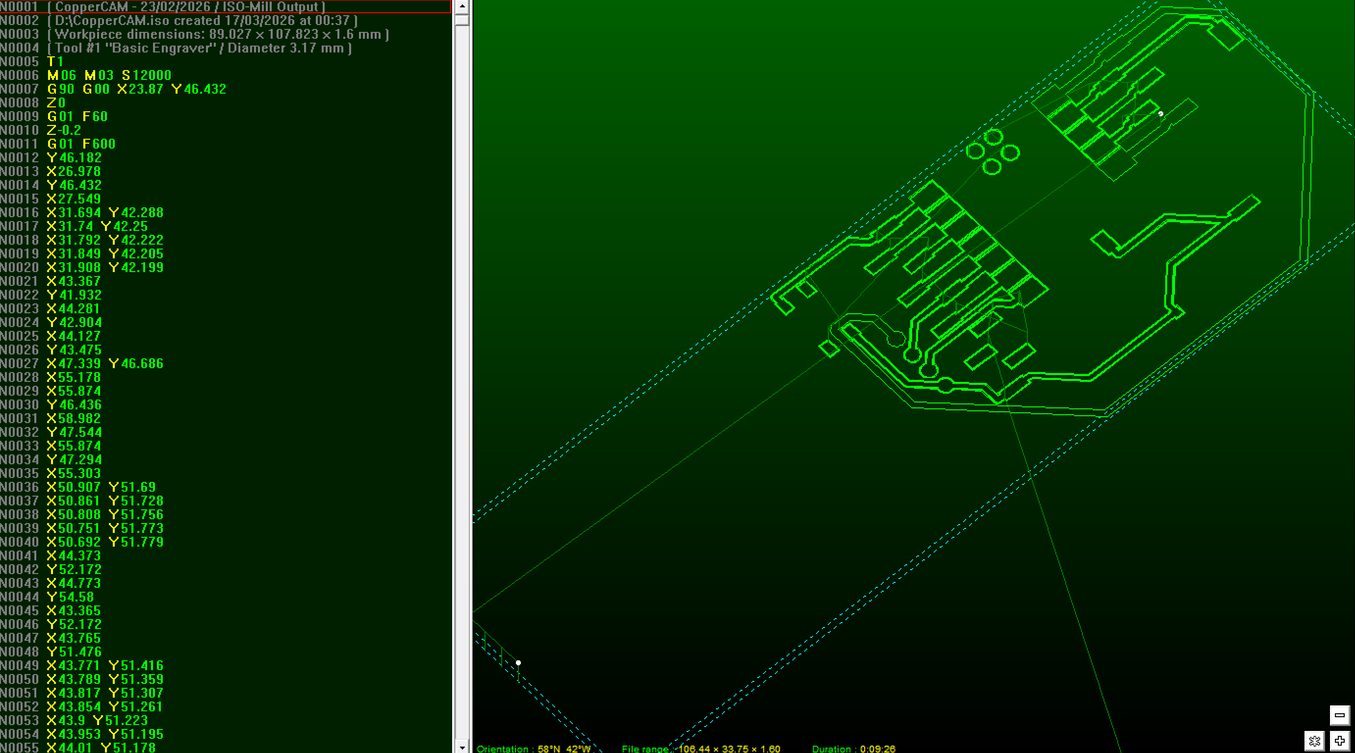
19 — Previewing the CNC Milling Path and G-Code
The PCB machining instructions were converted into CNC-compatible G-code for the SRM-20. The simulation preview displayed both the milling path and the coordinate-based machine instructions. The left side of the interface showed the sequential G-code commands controlling spindle movement, feed rate, and cutting depth, while the right side visualized the toolpath geometry. This preview helped confirm that the generated machining sequence correctly followed the PCB layout before sending the file to the milling machine.
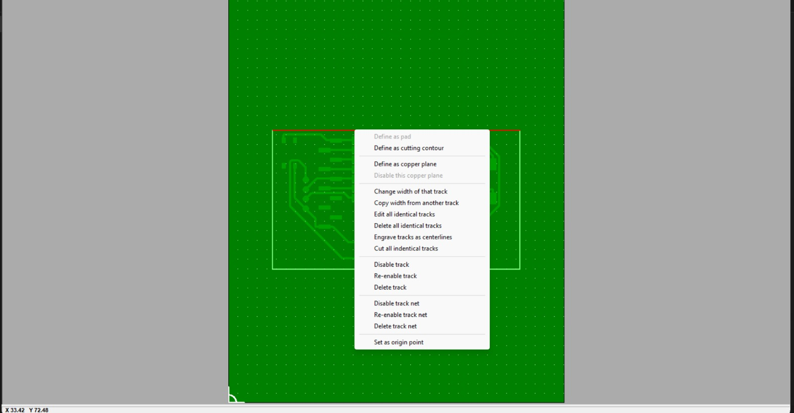
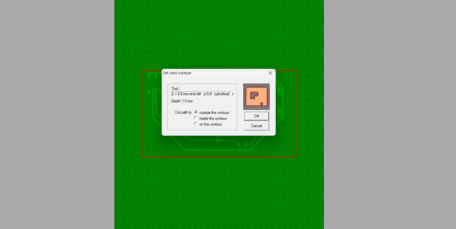
20 — Defining the PCB Board Cutting Contour
After preparing the engraving toolpaths, the outer boundary of the PCB was defined using the “Define as cutting contour” option in CopperCAM. This contour determines the final physical shape of the PCB after milling. Unlike trace engraving, the cutting contour operation uses a larger end mill capable of cutting completely through the FR1 material. Defining this contour is essential because it separates the completed PCB from the surrounding board material.

21 — Configuring PCB Outline Cutting Parameters
The cutting contour settings were configured using a cylindrical end mill tool with a larger diameter compared to the engraving bit. Parameters such as cutting depth and contour direction were selected carefully. The “outside the contour” option was chosen so the machine would preserve the exact PCB dimensions while cutting around the outer boundary. Proper configuration of these settings prevents dimensional inaccuracies and ensures a clean board edge after machining.
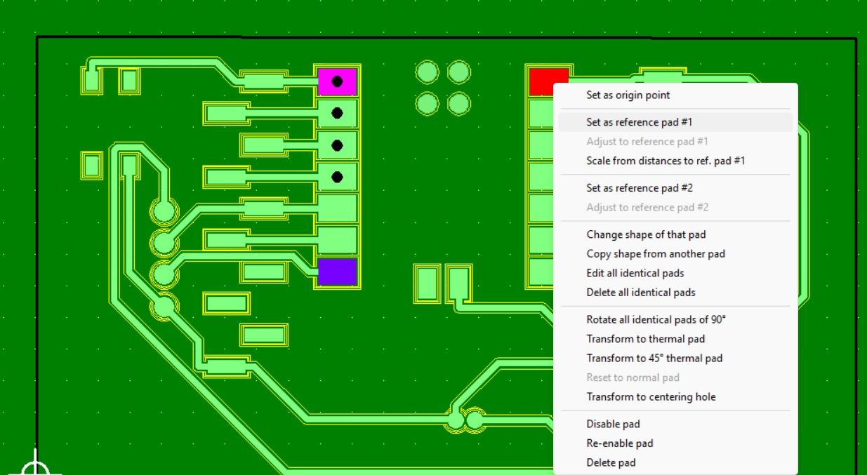
22 — Setting Reference Pads and Alignment Points
Reference pads were configured within CopperCAM to establish accurate coordinate alignment for the PCB machining process. These reference points are useful when adjusting machine coordinates, scaling, or repositioning the design relative to the physical board. Proper coordinate referencing improves machining precision and helps maintain alignment consistency between engraving and cutting operations.
23 — Final PCB Layout Verification Before Machining
Before generating the final machining output, the PCB traces, pads, and routing paths were inspected once again. The highlighted pads and trace network were checked for continuity, spacing, and overall geometry correctness. This verification stage ensured that the PCB design was free from visible routing errors and ready for physical fabrication on the SRM-20 milling machine.
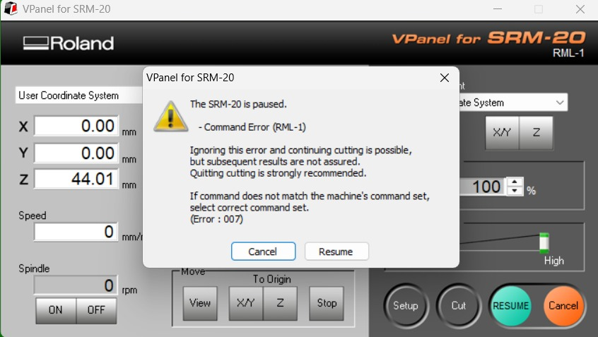
24 — SRM-20 Command Error During Machining Attempt
During the machining workflow, a command error appeared in the Roland VPanel software interface. The error indicated a mismatch between the machine command settings and the generated machining file format. The machine paused automatically to prevent unintended movement or inaccurate cutting. Troubleshooting such issues is an important part of PCB production because communication settings between CAM software and CNC hardware must match correctly. Resolving this error required checking the machine mode, output format, and command compatibility settings before resuming the operation.
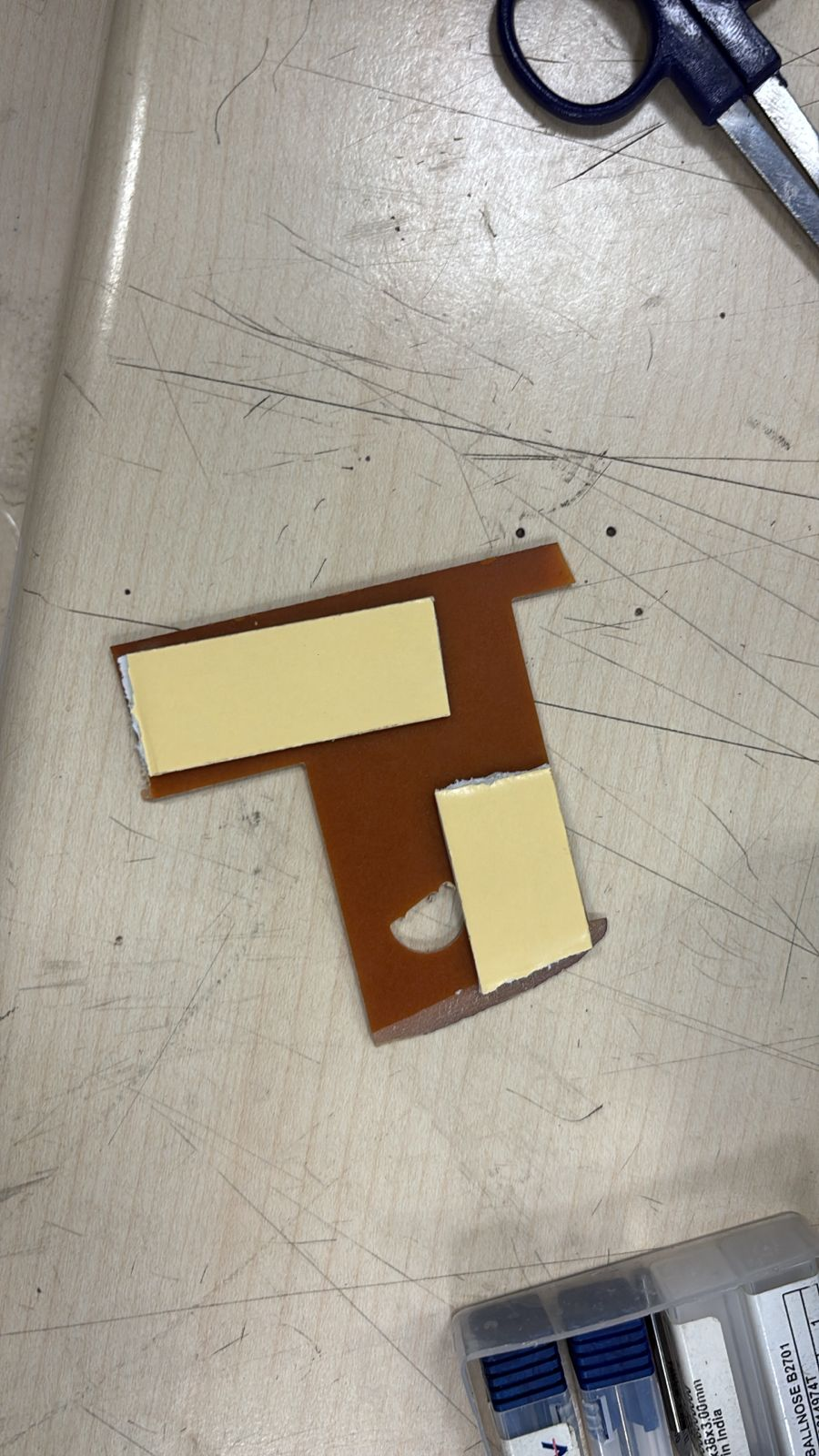
25 — Final Milled PCB on FR1 Copper Board
After correcting the machining setup and successfully completing the engraving process, the final PCB was produced on the FR1 copper-clad board. The isolation paths around the traces became clearly visible, showing the areas where copper had been removed by the engraving bit. The PCB contained routing traces, connection pads, and drilled regions required for component placement and soldering. This completed board represented the successful outcome of the electronics production workflow using the Roland SRM-20 PCB milling machine and CopperCAM toolpath generation process.