Week 6 - Electronics Design #
Hero Shot: #

TL;DR #
This week, I designed the PCB for my final project using KiCad. Before starting the PCB design, I tested the complete circuit on a breadboard using a Seeed XIAO ESP32-C3, NeoPixel Ring 16, DFPlayer Mini, and an 8-Ohm speaker to confirm that everything worked correctly.
I created the schematic and PCB layout in KiCad, solved a missing footprint issue for the DFPlayer Mini by importing external libraries, and adapted the design using pin sockets because the module footprint was through-hole instead of SMD. I then performed ERC and DRC checks, added mounting holes, configured custom track widths, created a GND copper plane, and completed the final PCB layout for fabrication.
Group Assignment #
Link to this week’s group assignment
Designing the PCB for My Final Project #
This week, I designed the PCB for my final project using the EDA software KiCad.
Before starting the PCB design, I first tested the complete electronics system on a breadboard to verify that all components worked correctly together.
Components Used:
- NeoPixel Ring 16
- DFPlayer Mini
- Seeed XIAO ESP32-C3
- 8-Ohm 0.5W speaker
After confirming the circuit functionality on the breadboard, I proceeded to design the schematic and PCB in KiCad.
video
Schematic Design #
I began by creating the schematic in KiCad.
One issue I encountered was that the DFPlayer Mini did not have a default symbol or footprint available in KiCad’s standard libraries. To solve this problem, I searched online and found a compatible symbol and footprint library from an external source.
I used labels to avoid confusion in the connections:
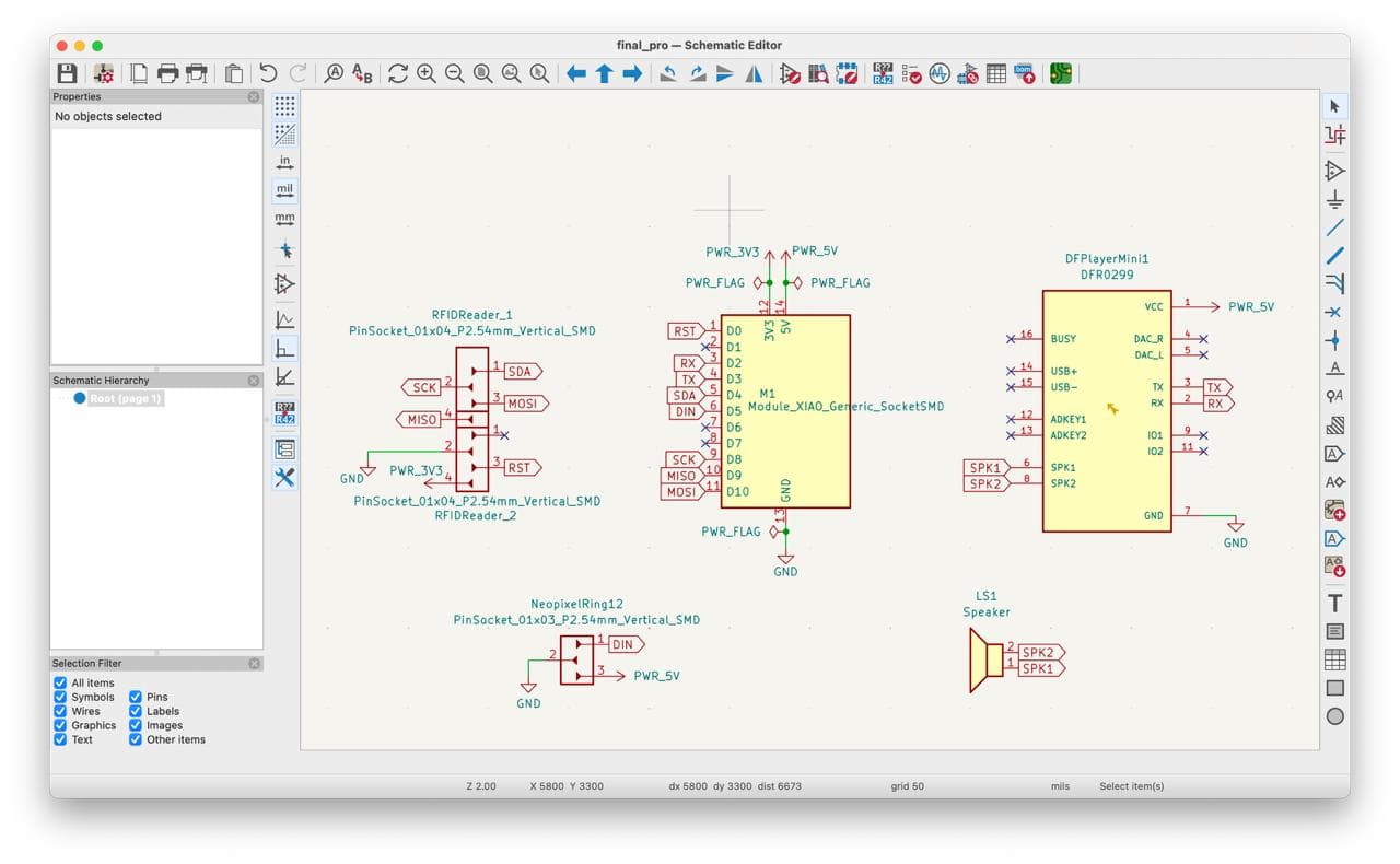
However, after completing the schematic and going forward with the PCB design, I realized that the footprint was designed for through-hole mounting rather than SMD assembly.
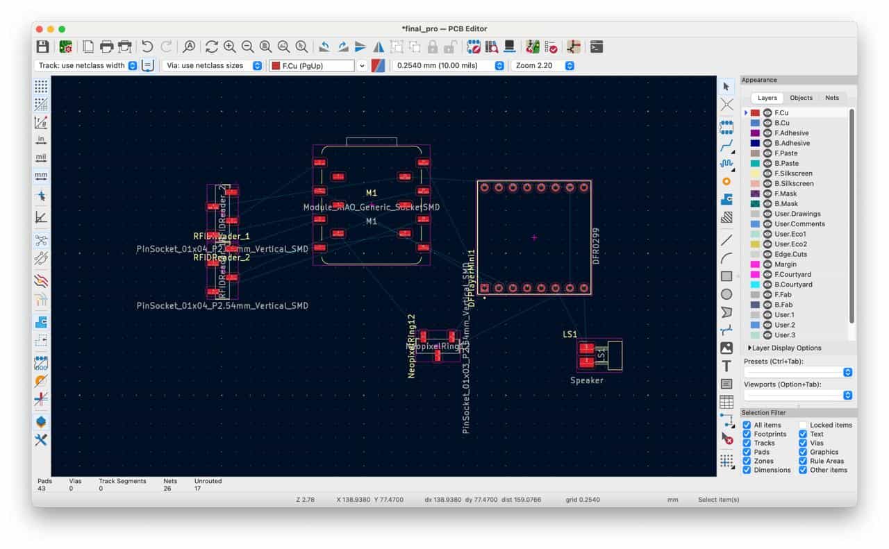
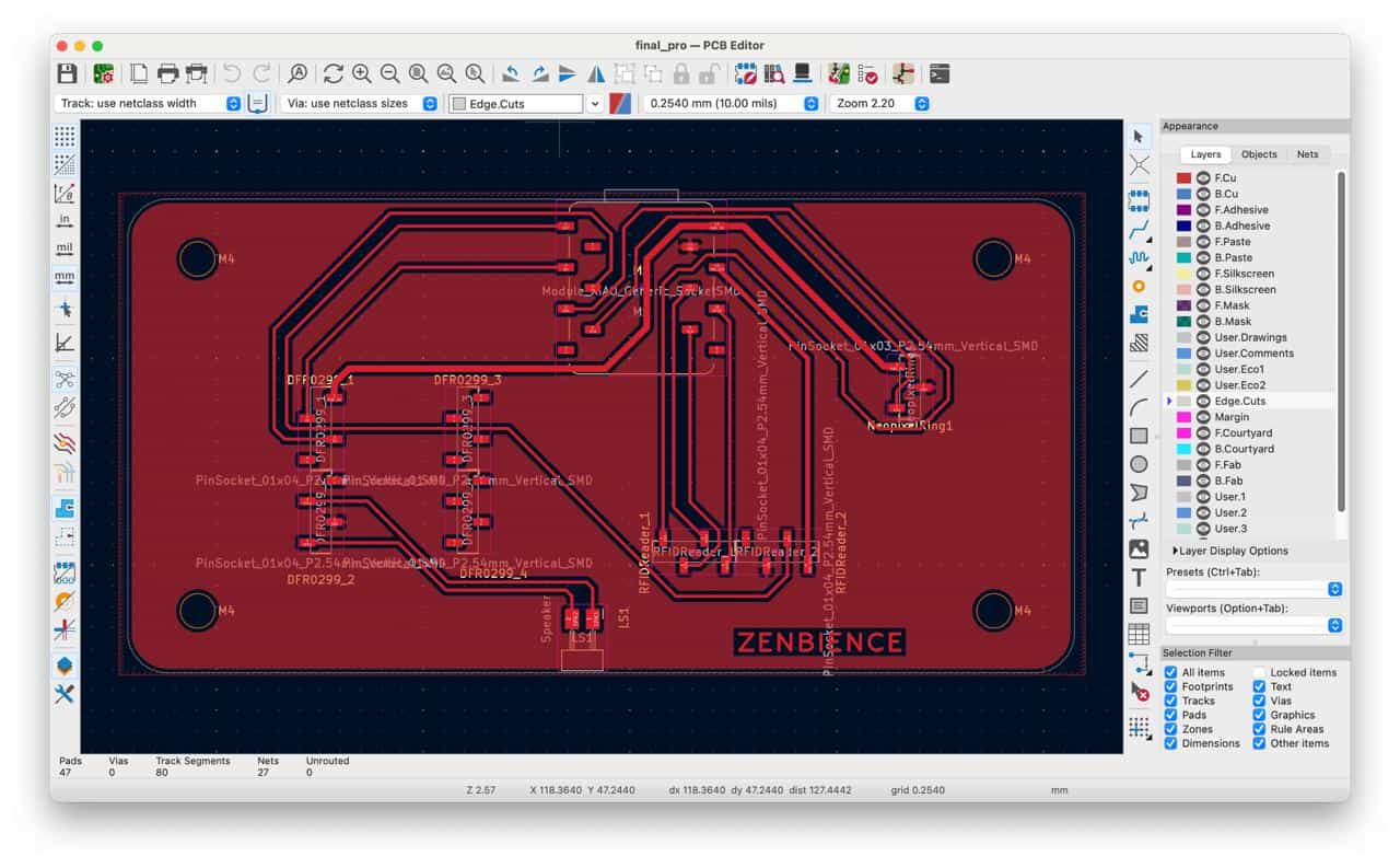
Because of this, I modified the design and added pin sockets to allow the DFPlayer Mini module to be mounted correctly on the PCB. I also added M4 mounting holes to the board so the PCB can be securely attached to the final enclosure.
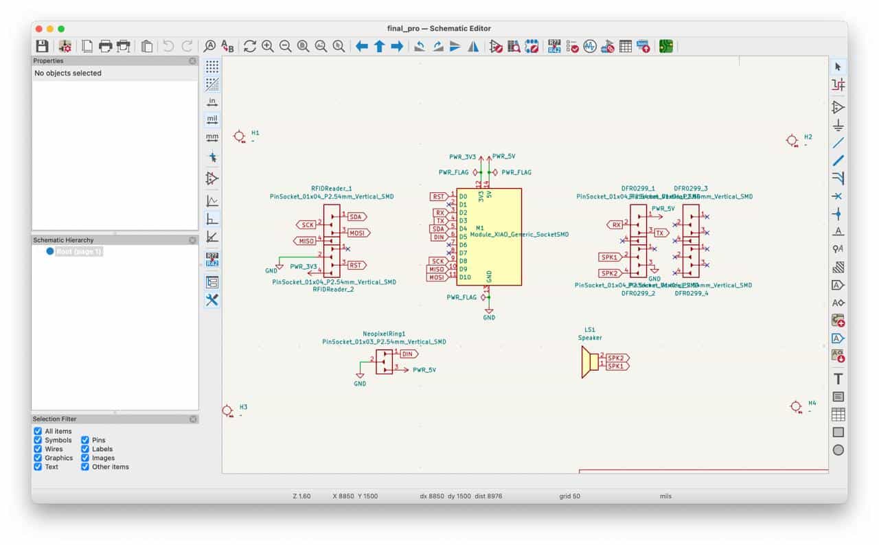
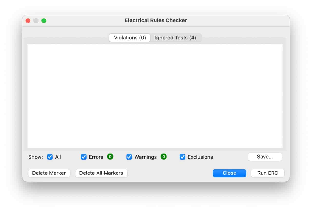
After finishing the schematic, I ran the ERC (Electrical Rules Checker) to verify that there were no electrical connection errors.
PCB Design #
Next, I switched to the PCB Editor and updated the board from the schematic.
From Edit → Board Setup, I defined additional custom track widths:
- 0.4 mm (default)
- 0.6 mm
- 0.8 mm
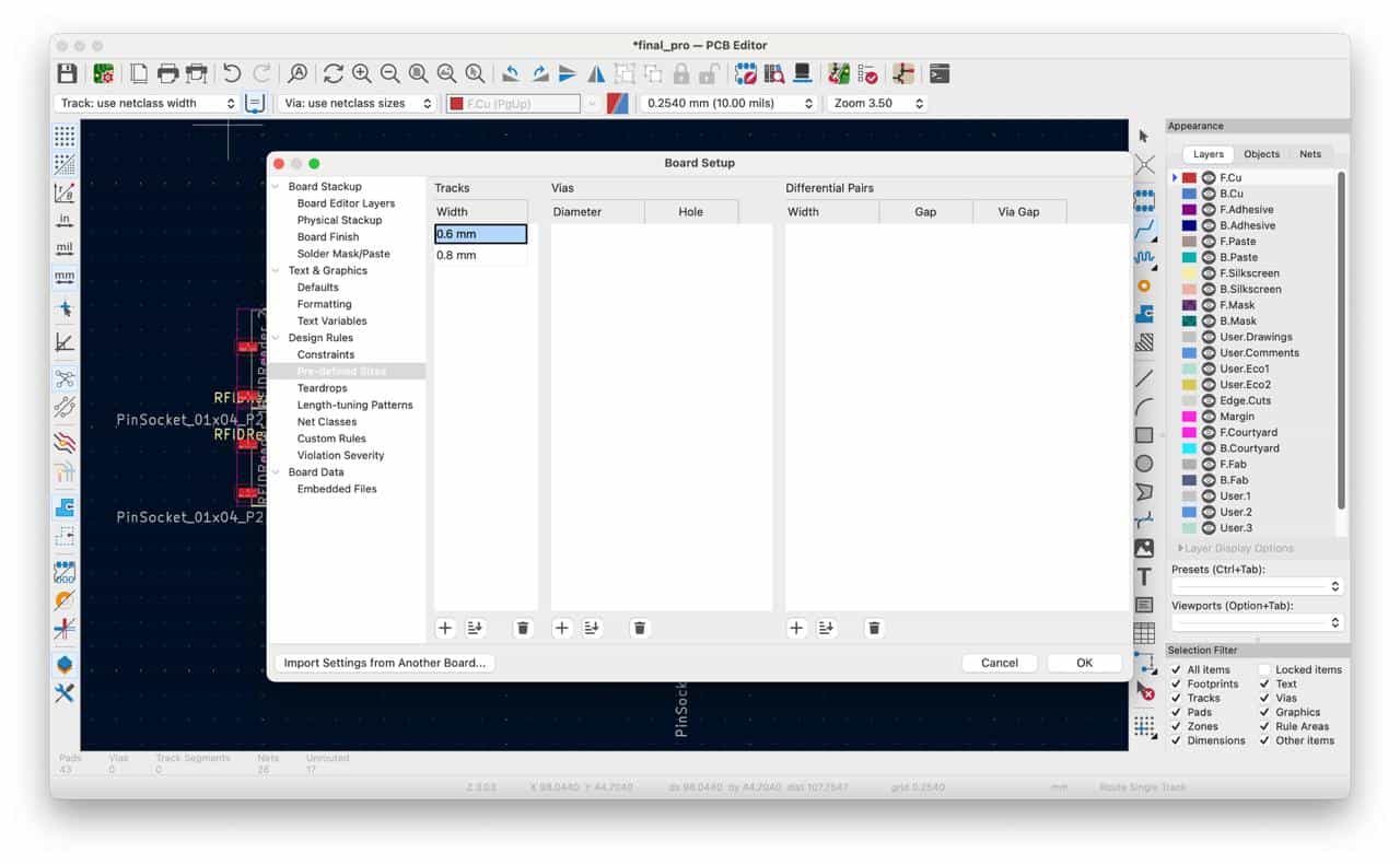
These wider traces helped improve power distribution of 5V and 3.3V.
I also adjusted the routing grid to 0.254 mm because the pin socket spacing matched this value, making component alignment easier.
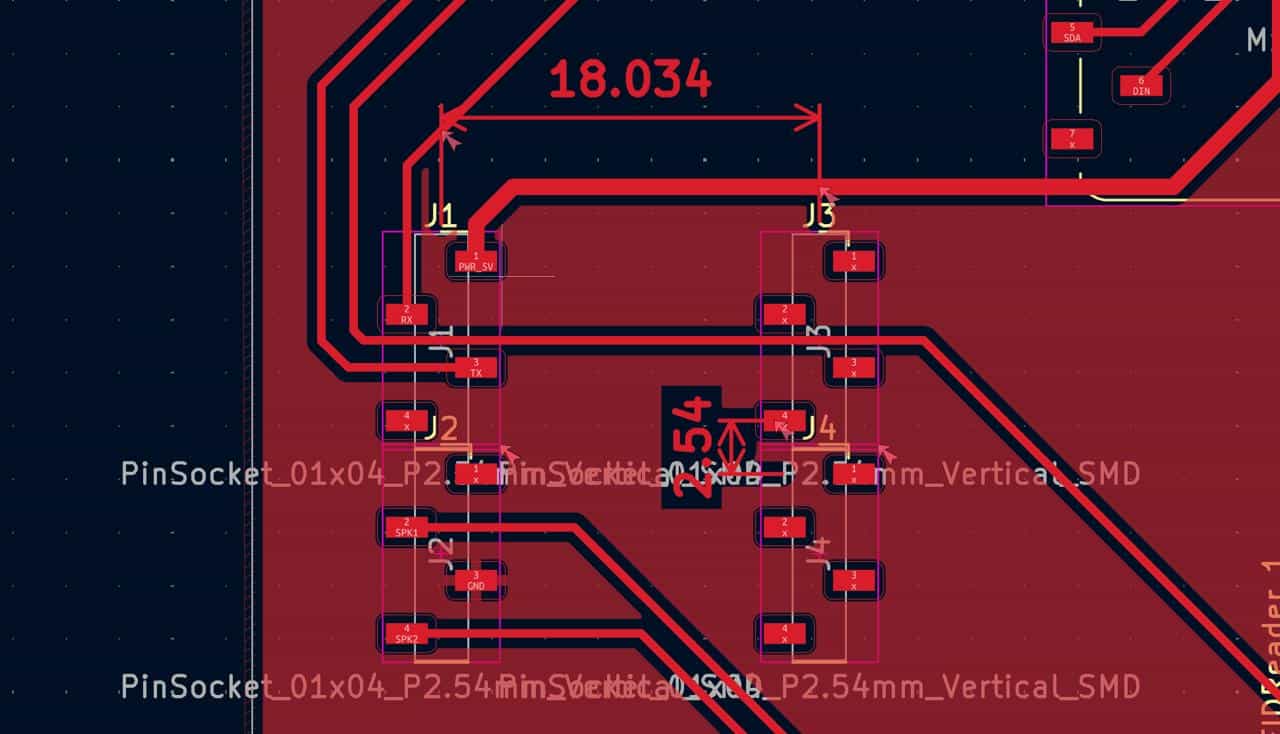
The Seeed XIAO ESP32-C3 was positioned at the edge of the PCB so that the USB Type-C connector remains accessible for powering and programming the board.
Routing the PCB was one of the most challenging parts of the design process. I needed to carefully organize the traces while avoiding isolated ground islands.
Maintaining a fully connected ground network is important for ensuring proper circuit operation and reducing electrical noise.
After routing the traces, I drew the board outline and created a copper fill zone connected to GND to form the ground plane.
Finally, I ran the DRC (Design Rules Checker) to identify any layout issues.
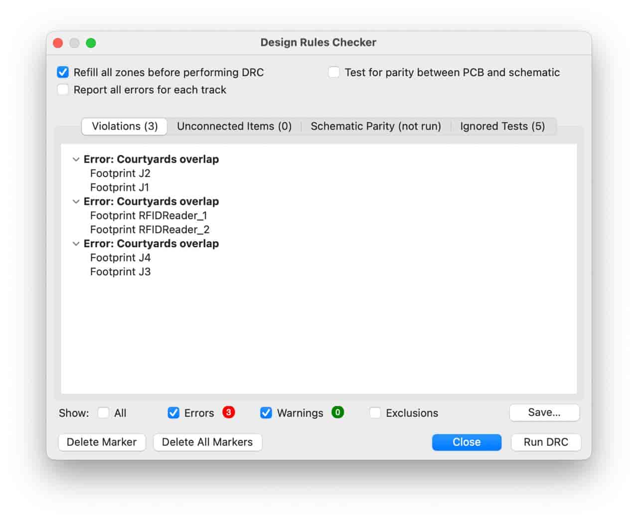
Some clearance warnings were expected because the pin sockets were intentionally placed very close together in order to fit all components compactly on the board.
After reviewing the warnings and confirming that the design was manufacturable, the PCB design was completed successfully.
Files: