Final project
Go To Documentation ›
Current state of progress:
- Download all
- README.md
- cad/omnipen-Bottom-v4.stl
- cad/omnipen-Tip-v4.stl
- cad/omnipen-Top-v4.stl
- cad/omnipen.FCStd
- claude-code/firmware/omnipen/inference.h
- claude-code/firmware/omnipen/model_data.h
- claude-code/firmware/omnipen/omnipen.ino
- claude-code/firmware/omnipen/weights.h
- claude-code/training/model_data.h
- claude-code/training/omnipen_model.tflite
- claude-code/training/train_model.py
- claude-code/training/weights.h
- pcb/IMU-board.kicad_pcb
- pcb/IMU-board.kicad_pro
- pcb/IMU-board.kicad_sch
- pcb/gerbers/IMU-board-Edge_Cuts.gbr
- pcb/gerbers/IMU-board-F_Cu.gbr
- pcb/gerbers/IMU-board-PTH-drl.gbr
- pcb/gerbers/omnipen_v1-Edge_Cuts.gbr
- pcb/gerbers/omnipen_v1-F_Cu.gbr
- pcb/gerbers/omnipen_v1-PTH-drl.gbr
- pcb/omnipen_v1.kicad_pcb
- pcb/omnipen_v1.kicad_pro
- pcb/omnipen_v1.kicad_sch
Starting point: a portable low-treshold notetaking tool
For my final project, I'm interested in experimenting with screenless human-computer interaction and interface.
I want to explore interaction more from the user's creative sources towards technology and less from technology to the user. I hope to empower the user to become more of a producer of new ideas and perspectives, rather than consumer of computer mediated ideas, and augmenting that process with technology.
My hypothesis is that leaving the screen out of the interaction frees up the user's vision to source more from their inner resources instead of being fully engaged by the interaction. There are many non-screen solutions with audio-based interface, but how about physical interaction?
I want notetaking to be as easy as possible. I think active notetaking is an excellent way to reduce information overwhelm as well as enhance thinking and creativity as thoughts can get externalized as they appear instead of trying to remember them. I want to make notetaking as easy as possible.
Requirements:
- Small enough to be carried anywhere with ease
- Connection to phone or computer (and cloud) for storage and organizing the notes
- There should be multiple documents to write on which can be toggled on the device
- Cheap(ish) to produce (there are a lot expensive devices for this purpose)
- Automated notes-to-text integration
The early chain of thought
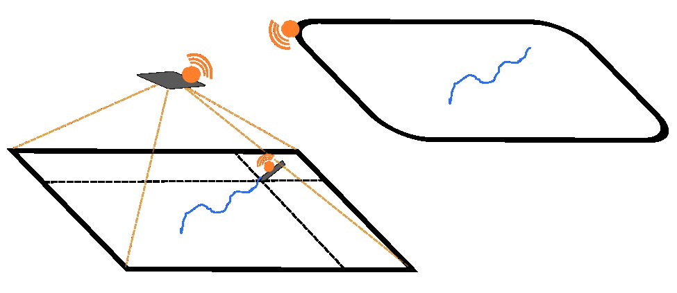
The earliest idea came from the first week:
A portable sheet that has sensors on the sides so that it
knows a
location of pen that is "drawing"
on the sheet. The pen has a sensor which senses the pressure. There is also a projector on
top of the
sheet, projecting on it what has been drawn. What is being drawn is also visible on
the computer screen (on the right). I'm looking into a possibility to integrate it into a
open
source design software, such as GIMP, Inkscape or even FreeCad.
I draw a sketch of this idea when I was practicing InkScape:
After discussing with Kris of this idea, he suggested that I'd make my own "rand tablet", an early version of a tablet and a stylus from 1964. Here's link to original paper and youtube video that explain how it works: it sends a pulse in speficic times to each wire under surface. The pen senses pulses, sends them to computer through wire, and based on which time-coded pulses it receives, an accurate position of it is calculated and its input controls the software.
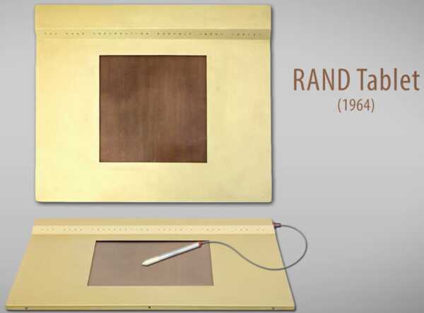
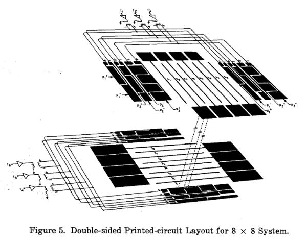
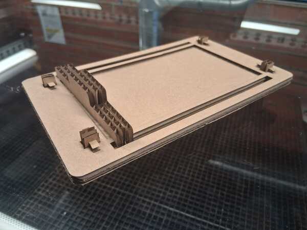
Followed by this chain of thought I made a cardboard prototype of it (or similar at least) in the laser cutting week. It has an integrated swipe for cleaning up the surface.
Idea: Pocket-sized note-taking device
A small tablet type of device that can fit into pocket and has a pen that leaves an impermanent mark on the surface (or doesn't).
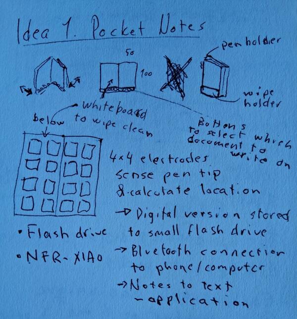
Claude gave a simulation of this as we were discussing with it tp make sense of the Rand Tablet (see below).
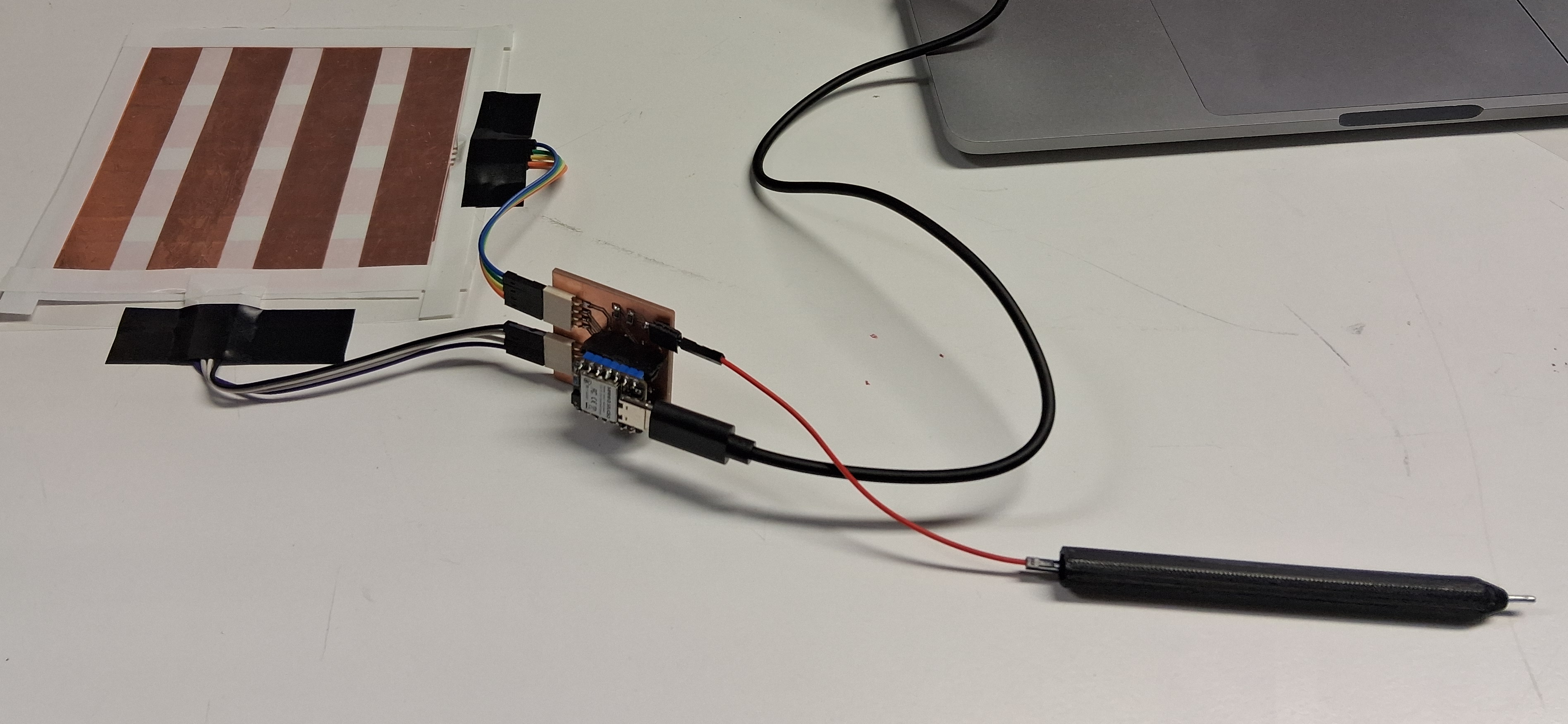
I continued exploring this idea in the Week 8: Input devices and made a capacitance sensing platform out of copper stripes and epoxy tape as well as a 3D printed "pen", but I couldn't make this idea work and left it to be able to continue to other things.
Idea: Universal pen
A pen that can write on (almost) any surface and it saves the notes based on where the pen tip has moved.
Here's a paper on FlashPen that does something similar with an high-accuracy optic sensor as in a gaming mouse.
After being selected by random selector in the review part of the global lecture, Neil mentioned that an optical sensor is not accurate enough and I should use an IMU sensor to spot patterns in the pen movements.
This idea led to the idea of my Final Project.
A pen is a device with long and tested history of making human creativity into reality and even today almost everyone rely on it at some point. How could we enhance pen's simple yet powerful design with technology, without reducing its original purpose?
The Idea: Omni Pen
A pen with which I can write on any surface, have the text output saved in digital format and eventually be sent wirelessly to another device to view.
With this pen I can add popping ideas to my notes anywhere and anytime without having to carry a notebook etc. with me: all I need is a flat surface.
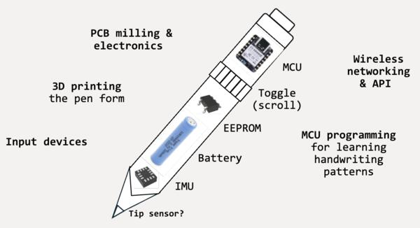
* Update: Toggle (scroll) is going to be a button on the top end with RGB LED on the side
Bill of Materials:
| Components | Source Link | Amount | Price (appr.) |
|---|---|---|---|
| Microcontroller: XIAO nRF52840 Sense (6 Axis IMU, bluetooth, CPU performance) |
Digikey | 1 | $16.00 |
| Inertial Measurement Unit (IMU): LSM6DSOXTR
(This smaller one to be placednear fingers) |
Digikey | 1 | $5.00 |
| EEPROM Memory: 24LC32AT-I/OT | Digikey | 1 | $0.44 |
| Battery: Power plus ICR10440 AAA 3.7V 320mAh | Suomen Akut | 1 | $15.00 |
| Battery protection IC: DW01A | Digikey | 1 | $0.10 |
| MOSFET N-CH 30V 5.2A SOT23-3 | Digikey | 1 | $0.82 |
| 4,7kOhm Resistors | Digikey | 2 | $0.20 |
| 0.1 uF Capacitor | Digikey | 1 | $0.10 |
| FR2 for PCB and/or copper and epoxy tapes | ~ $1.00 | ||
| PLA (FFF) and/or Resin (SLA) for 3D print | ~ $1.00 | ||
| Total | ~ $40 |
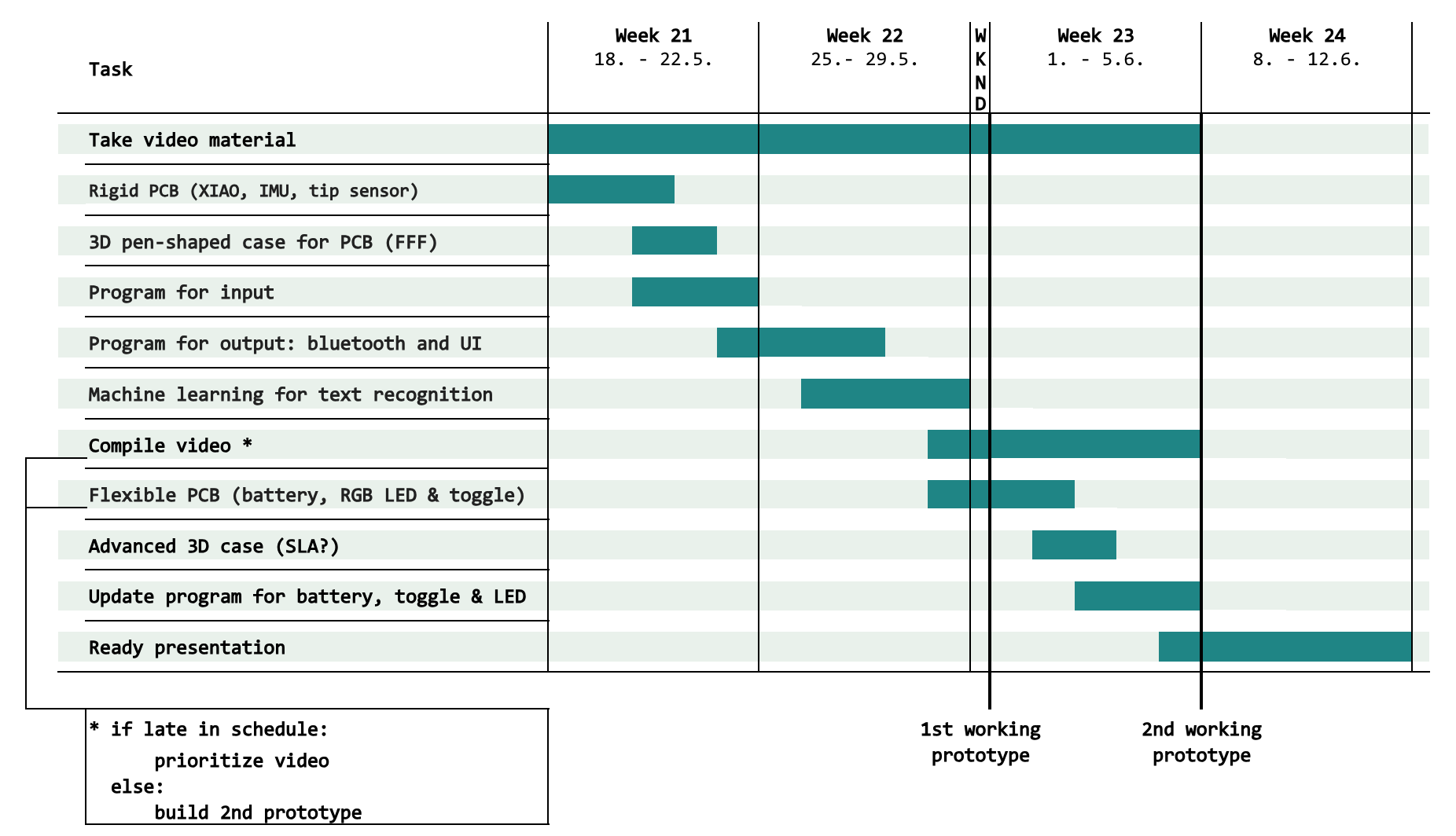
Timetable:
Future possibilities
- More sensor precision to qualify for catching free handwriting and drawing.
- A widget to be attached on any pen that does the same + leaves the markings of the original pen.
- An augmented reality application that shows with phone camera what was written on a surface (allows for example secret writings).
Log: Development process
I began to design the first prototype with KiCad as I knew which components were needed. Having the components on a board helps in designing the first 3D print. However, I don’t yet know how is IMU, battery, or EEPROM is used in a PCB. Also how do the components in the Fablab Kicad library correspond to the components I’m using.
So I began a conversation with Gemini about the components, PCB schematics and what needs to be taken into account.
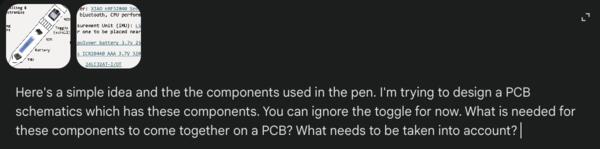
The main takeaways from Geminis answer were:
- IMU and EEPROM communicate through I2C so there’s a need for different addresses. Also pull-up
resistors (4.7kohm) for both of these are needed to have a signal working with their pins.
- For the battery, a capacitor (0.1 uF) is needed and placed near the VCC pin of IMU and EEPROM to
reduce noise (for pattern recognition). Also having battery protection IC is important in preventing
electric shock as it is near the users hand.
- Double sided PCB is needed because it’s so thin.
- For getting the benefit of dual IMU (integrated to the XIAO and the external one), such as knowing the
angle of the pen, the IMUs should be placed in parallel on X-Y-Z axises (no need for converting the data
to match). This means the external need to placed as the XIAO because XIAO is bigger and have less
freedom in placement.
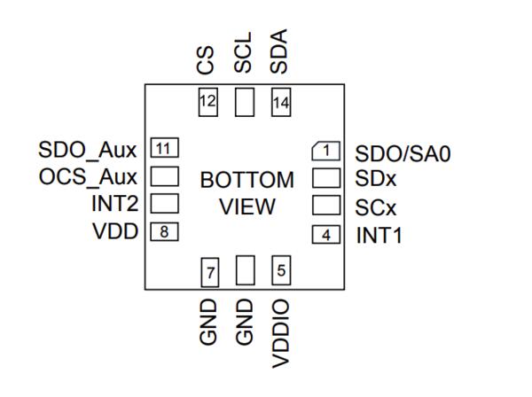
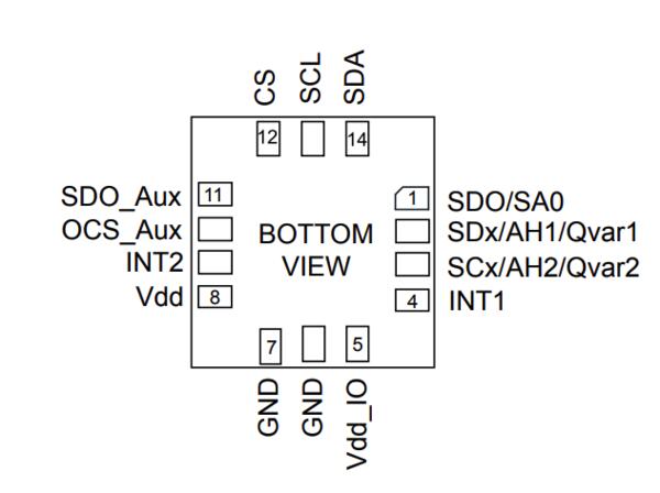
I opened KiCad as, to begin with testing the whole idea, I needed to make a PCB that has XIAO and IMU. The IMU I’m planning to use is named as LSM6DSOXTR and the IMU in KiCad is called LSM6DSV16XTR. There are similar letters but I’m not sure if their pinnings are similar enough to model a PCB on. Comparing their datasheets, they seem to be same enough to be used in KiCad.
LSM6DSOXTR (the one I’m using)
LSM6DSV16XTR (the one on KiCad)
Electronics design
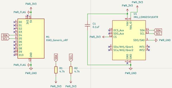
As I didn't know well how the IMU works, I asked Gemini to get me started: I wanted to make it as simple as possible so that the XIAO and IMU work together. The IMU is connected via I2C pins, i.e. SDA (D4 or pin 5 in KiCad) and SCL (D5 or pin 6 in KiCad). Also, Gemini says that there’s a need for decoupling capacitor for the IMU (between 3.3V and GND). This was the initial schematic that I asked for Gemini if it looks correct.
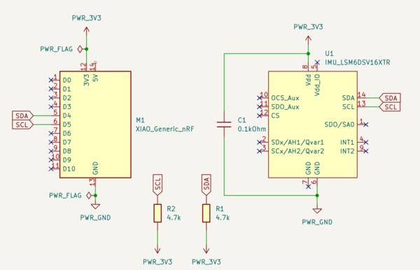
Geminis reply demonstrated that I still didn’t know how the IMU is used on a PCB.
The issues were:
- Vdd pin powers the IMU sensors but SDA and SCL are powered through Vdd_IO pin which I had marked
crossed
- CS pin tells the IMU whether to use SPI or I2C, and having it HIGH means I2C is in use. Gemini
suggests connecting it to 3.3V to have it HIGH all the time, and I decide to do that (at least for now).
- SDO/SA0 (pin 1) should also be connected to 3.3V or GND to define the address of the chip for the I2C
bus. It’s the only address used so it doesn’t matter which one, I set it to GND.
After fixing these issues, the schematic looked like this:
Brought up by Gemini, I came to think if the design should be two boards connected by a cable (eg. FFC) instead of one rigid PCB. Then the structure of the pen relies more on 3D printed shell. Discussing further with Gemini about the cables, the main issue with the connections seems to be intermittent signals and electric noise (which are also why my protoype of a touchpad likely failed a few weeks ago).
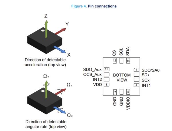
This depends also of the directions of the two IMUs in case the IMU needs to be placed in different orientation to the XIAO, eg. turned 90degrees, which would exclude rigid PCB. Asking about the orientation of the two IMUs, Gemini’s answers were hallucinated as I checked the LSM6DSOXTR datasheet which has a clear image of the orientation (below).
It was more difficult to find information about which way the (similar) IMU is placed inside the XIAO. This would be relatively easy to test, but I lost my electronics yesterday by mistake and haven’t yet replaced them.
Here are two picks from the Gemini reply: flexible wires twisted together or flexible PCB.
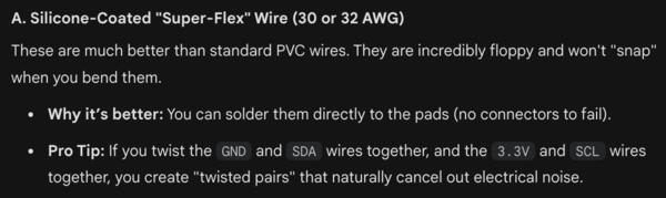
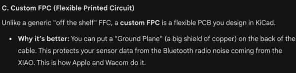
As the first iteration focuses mostly on testing the whole concept, having the wires twisted together is probably better option than a rigid PCB regarding the noise. For the final design a vinyl cut flexible PCB with a ground copper layer is a good option. It seems the connectors are a likely weak link what comes to using cables.
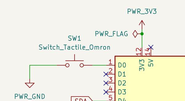
For adding buttons and the LED on the PCB I went to check my documentation from Electronics design week to remind how I made the PCB with buttons and LEDs. So, I need to add the Pin.PULL_UP parameter on the pin and then I don’t need an actual resistor on the board. I noticed that I had connected power supply to 5V so I changed that to 3.3V as well.
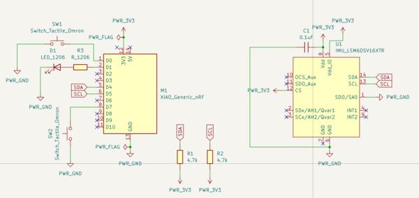
Then I also add the RGB LED with resistor and the other button that becomes the tip sensor. Here’s the overall view.
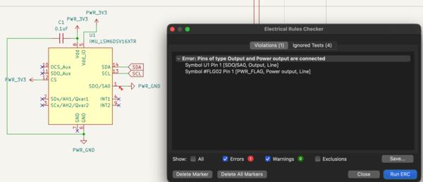
Running DRC, I get the following error. I ask Gemini what’s it about because it had guided me to connect that pin to either 3.3V or GND. It explains that in the schematic library the pin is defined as output because if using SPI the pin act as output (Serial Data Out), but using I2C it is Input pin, defining it’s address based on voltage coming in to the pin. I check this answer from the IMU datasheet (accessed at digikey component page https://www.digikey.fi/en/products/detail/stmicroelectronics/LSM6DSOXTR/9841882). And in there is the same explanation.

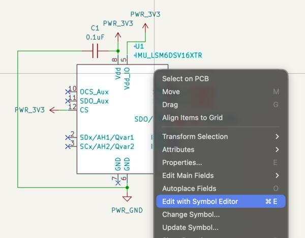
The solution is to change the library default: right click the IMU part, select Edit with Symbol Editor, double-click SDO/SA0 pin, and replace Output with Bidirectional or Input. OK and save changes.
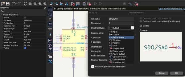
Now the DRC shows the issue only as two warnings.
I go to the PCB Layout Editor and spread out the components to get an idea of their dimensions etc. I come to think further about the RGB LED which was now placed on the schematic as a simple LED as I got confused of the RGB LED schematic while the actual component was so small. I go back to Schematic Editor and replace the LED_1206 with LED_RGB. I check from my Electronics design week documentation how the resistor strengths were calculated for the LEDs. I again find the digikey resistor calculator and from the RGB LED datasheet I find the values to put to the calculator.
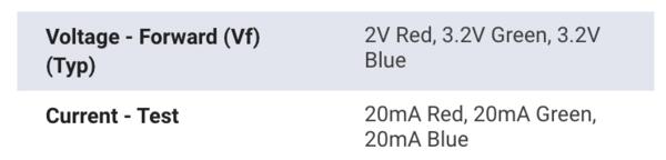
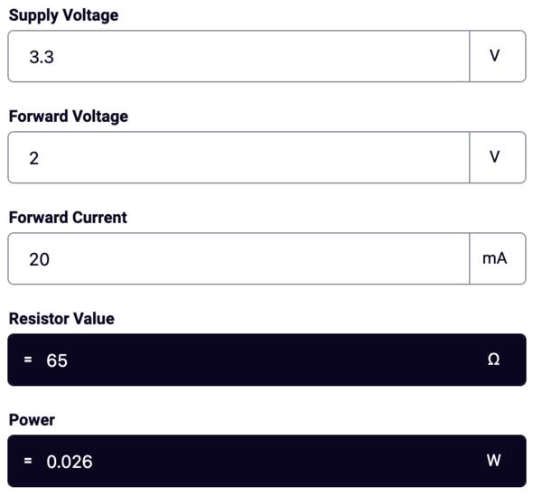
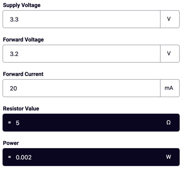
Green and blue get 5ohm resistors and red gets 65ohm resistor, which becomes 49.99ohm because those are in the inventory, so red light shines a bit brighter. I place and connect them on schematic editor. I was unsure how to connect the RGB LED so I asked Gemini and it confirmed that I had done it right. (The resistor values are still incorrect on the image)
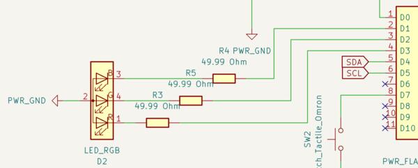
But in addition, Gemini also noticed my resistor values and noted that they are quite low and that the given 20mA is quite much both for the microcontroller and the battery (roughly calculating for 320mAh battery, with white color (3 times 20mA) it would take 5 hours to drain the whole battery only by the LEDs). Also the nRF52840 has a limit in how much current is good to let out of a pin and according to Gemini (and google search) it is 15mA and in the datasheet page 84, if I understand correctly, it is 25mA in high voltage mode.

Anyway, Gemini suggest using 5mA forward current and then the resistor values would be, first in theory and then in Fablab inventory:
Red 260 ohms -> 499 ohms
Green 60 ohms -> 100 ohms
Blue 60 ohms -> 100 ohms
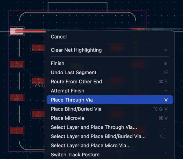
I’ve been thinking that I should make this board double-sided to keep it as narrow as possible and have both the buttons and led on the other side and the microcontroller and IMU at the other. A route can be made to other side of the board by placing a via: in KiCad that works by selecting Route-tool (X) and right-clicking on the spot where the via should be in and selecting Place Through Via (or Left Click + V). The components can be placed on the other side by by selecting the component and pressing F. The colors changes from red to blue.
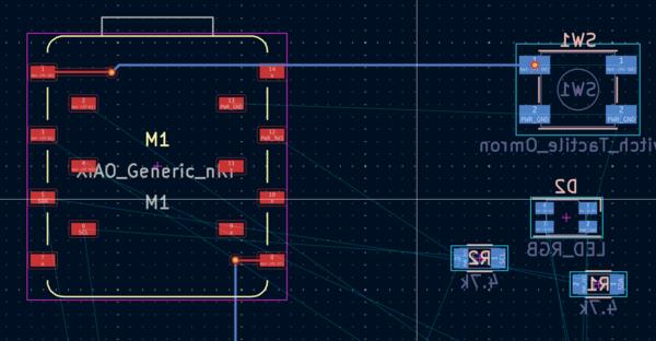
Kris told me that the single IMU part needs to be cut with laser as the footprints of the component are so thin. Instructions for that can to be found at Kris’s gitlab. This would bring some extra complexity to the process, and as I have less than two weeks now left to make the first prototype, I decided to use Adafruit’s LSM6DSOX 6 DoF Accelerometer and Gyroscope which has ready-made board with good instructions.
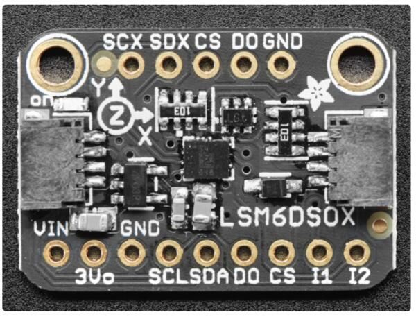
I don’t know how to add the component to the KiCad schematic as I can’t find anything similar in our inventory library. I googled “How to place Adafruit LSM6DSOX to in kicad schematics?” and it appeared that I should create a custom symbol at Symbol Editor. I ask Kris what should I do, and he says that I should do the same what I did for ToF board: measure it’s dimensions and place pinsocket accordingly. But I don’t want to make it that large as that would increase the height by over 10mm. Then Kris suggested to tape the board on the other side of the PCB and connect the pins with small wires through vias on the board. So I will do that.
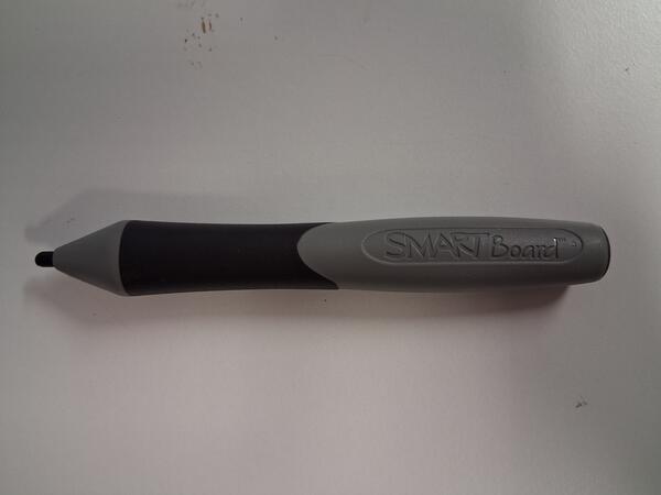
I have this smart board pen as a reference for the size that is still comfortable to the hand. Having these components inside the pen I need to have slightly wider case but it’s still tolerable to use.
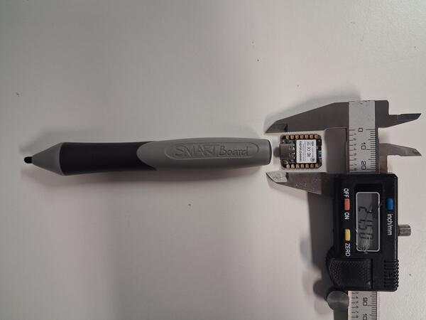
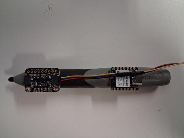
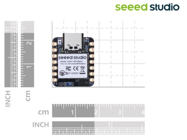
I start by removing the IMU and capacitor from the layout and schematics and then open my week eight documentation on Adafruit's ToF and Adafruit’s LSM6DSOX materials to check the dimensions aas well as its datasheet to figure out the IMU position in it. It appears that the dimensions are the same as ToF is also Adafruit’s board but the pins are different.
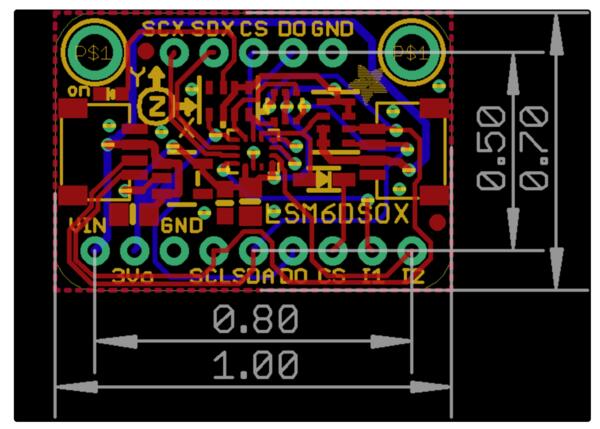
The position of the IMU seems quite difficult to find so I quess I just need to test it by myself. This is necessary because I would want this IMU and XIAO’s IMU to be aligned so their output data is easier to combine (if necessary) without any coordinate conversion. Actually the pattern recognition might work even with differing coordinates. And now I also remember that I dont’ know the IMU position in XIAO board either. Well this is not that important anyways.
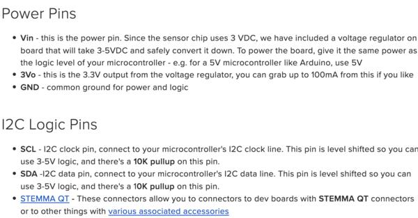
Now looking at the pin explanations, I wonder how QT STEMMA connectors work and whether I could use those instead of the rather complex solution with the pin soldering through vias.
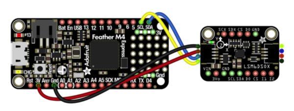
At first, it wasn’t for me very apparent where those connector are connected within the board but then I found this example image further on in Adafruit’s LSM6DSOX materials.
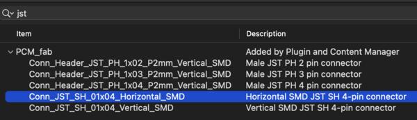
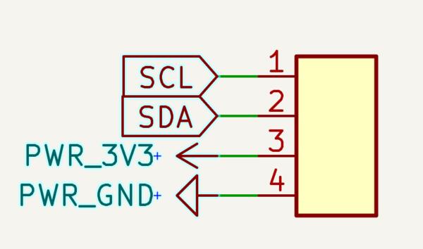
I go back to KiCad and replace the IMU and capacitor with a JST SH horizontal connector and place the correct labels.
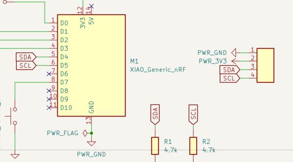
In the Layout view I notice that the labels on the connector seems to be in wrong way compared to the schematic view (see above image). One explanation can be that the layout image should actually be rotated 180 degrees but I don’t think this is the case as I have already used a connector a few times this way. So I change the labels in Schematic view to the following.
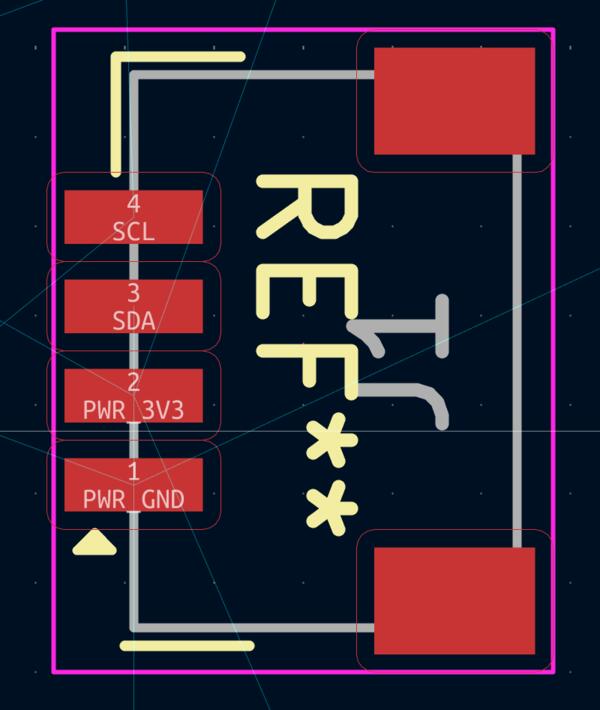
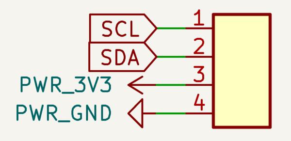
Now thinking about the buttons and the two-sided PCB… The rigid PCB does not necessarily need to reach the tip end of the pen anymore as IMU is connected with wires. Also the tip sensor is not an actual button but a 3D printed tip with spring and its connection is placed on XY-plane instead of ZX-plane like the XIAO and IMU. Thus having a rigid PCB for the tip sensor doesn’t seem very suitable. So I guess I could use wires and connector for the tip in this first prototype. If I use flexible PCB in next iteration then bending the routes to XY-plane for the buttons is easier.
I add the tip sensor connector to the schematic. I asked Gemini what does the UPDI mean in the connector name but in the context of a simple wire connector it isn’t relevant.

What comes to the top end button, it is also on XY-plane as the button is top down and there is also a spring under the 3D printed button so that it bounces back (the 3D print should be made so that it makes “a click” when pressed for haptic and audio feedback and the LED color changes as well). But the toggle button was scheduled to be only in the second iteration so I decide to remove that from the schematic for now.
The PCB now becomes quite simple. ERC shows no errors.
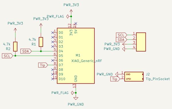
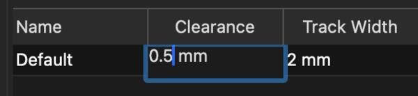
On Layout editor, it seems that I cannot make the PCB only as wide as the XIAO board or DRC shows errors everywhere. The narrowest that I was able to make without errors was 21.5mm and even then the Fill zone doesn’t reach the GND pin. That’s getting quite bulky for a pen already.
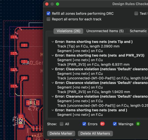
I come to think of built-in resistors and after checking, I actually don’t need the pull-up resistors now on the PCB as Adafruit LSM6DSOX’s SDA and SCL have 10k built in pull-up resistors. So I remove them and the PCB becomes even simpler.
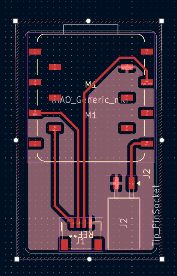
I think to have the board as narrow as possible I’ll make it double-sided and have the bottom for GND. I actually need to do the double-sided pin soldering for the XIAO, because I don’t want to use the large pin sockets for connecting the pins to the PCB.
I realized that I can go round the GND pin to have it connected properly. Now DRC shows no errors.
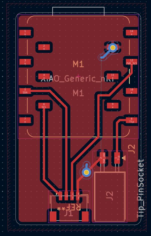
Now I was thinking of adding vias on the pins that I’m going to use but realized (remembered) that the pin locations are mirrored when the XIAO is turned to the bottom side of the PCB. Also the pins shown in the KiCad Layout editor don’t represent their actual locations. Looking at the XIAO dimensions, it looks like the pin hole is 1mm wide and it’s border is 1mm from the edge of the board.
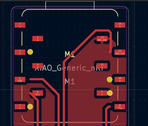
I make 1mm vias to the other side of the PCB that the pins that I use are located, like this:
Then I remove the XIAO board from the Layout to get rid of the errors. This feels like some sort of KiCad blasphemy.
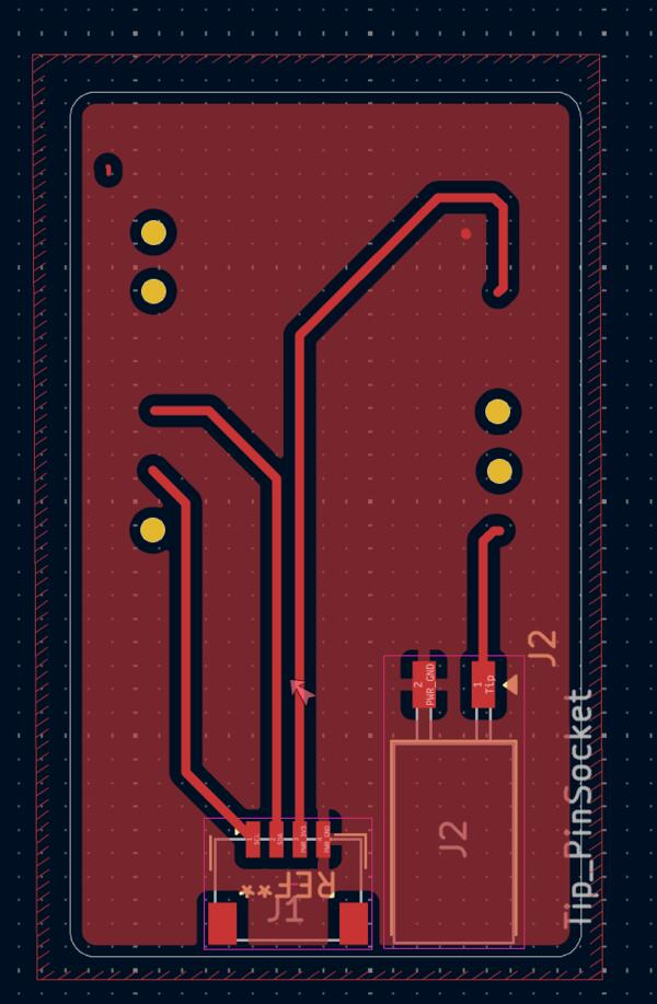
I had forgotten to make a via for GND pin.
And now I notice that the 3.3V route goes over the via for GND pin and that becomes a problem when I make the board as narrow as the XIAO board. I solve this by having the ground on the flip side of the board and make vias for the grounds from the connectors.
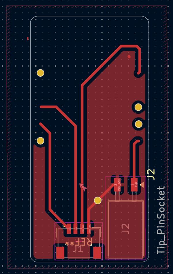
Now all the vias have errors that I don’t understand so I ask Gemini. The problem was in net class settings: I had both via size and via hole 1mm and as I doubled the size there was space for the copper around the via.


Now there are only warnings that are alright.
Now in the morning, I was clearly tired yesterday evening when making this thing because, as now looking at it with fresh eyes, of course the routes on F.Cu need to be connected to the vias. So I do that.
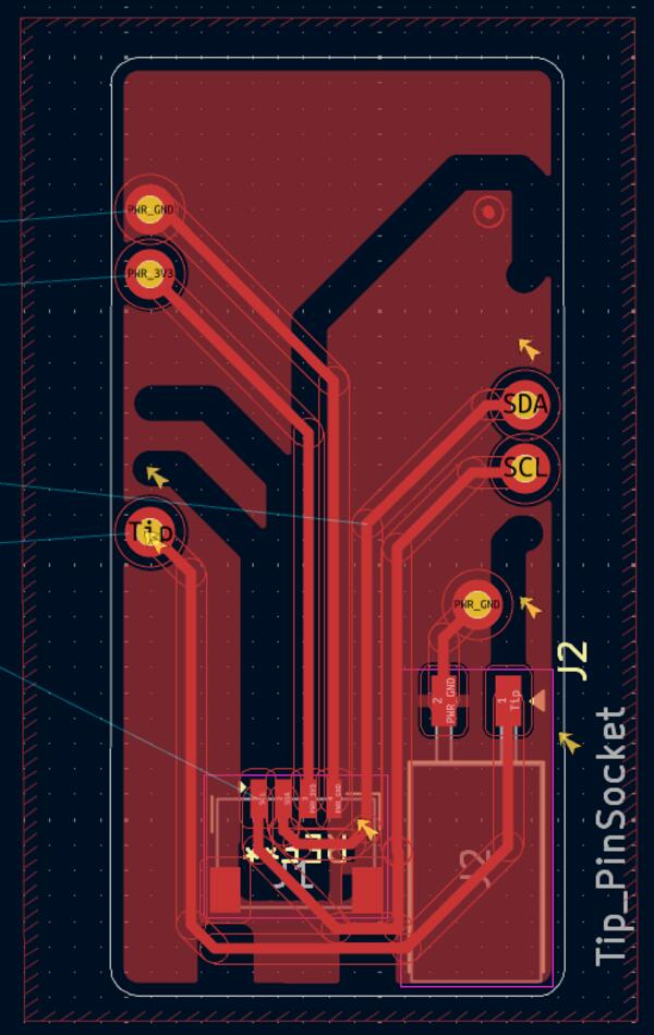
Thinking about the pin locations, relying on KiCad Layout is not probably a good idea. I can’t find a proper dimensions of a XIAO board but I calculate that pin’s centers are 2.5mm away from each other and 3mm from the edge because the whole legnth is 21mm and 6*2.5mm + 2*3mm = 21mm.
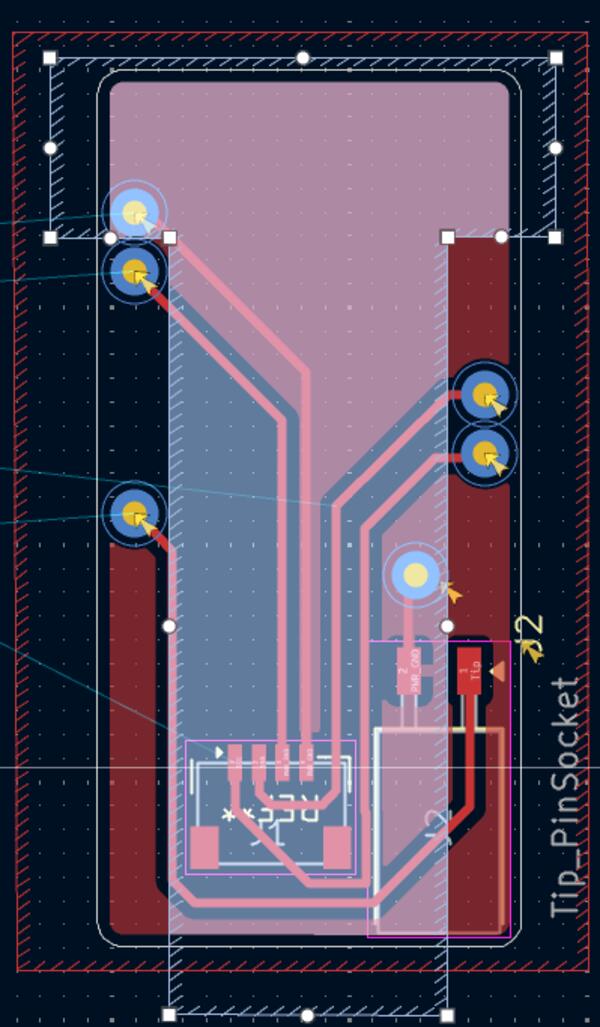
After placing the routes to the vias, I place the fill zone to B.Cu as GND to cover everything except the areas of the pins so that they don’t accidentally touch the ground. As there are no problems in DRC, I believe this to do the job.
The pen shape
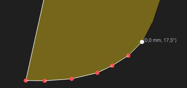
I continue to Inkscape to make a shape for the pen based on the reference pen that I have. I open the image on one layer and on another layer I use the Pen Tool to shape half of the pen. Then I straighten it up, resize the page to the shape and export it as svg.
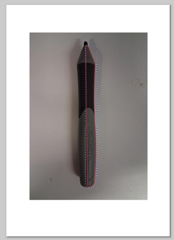
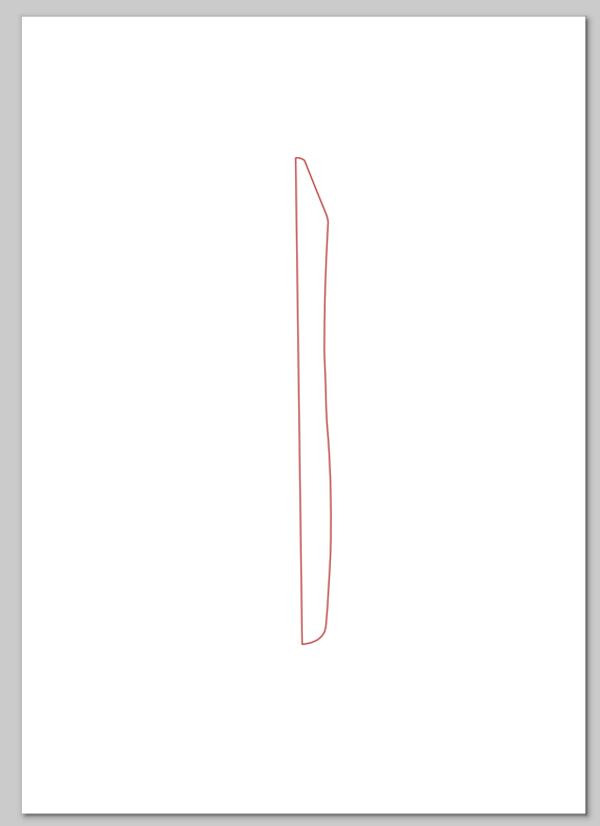
Then I import the image as SVG as Geometry to FreeCad.
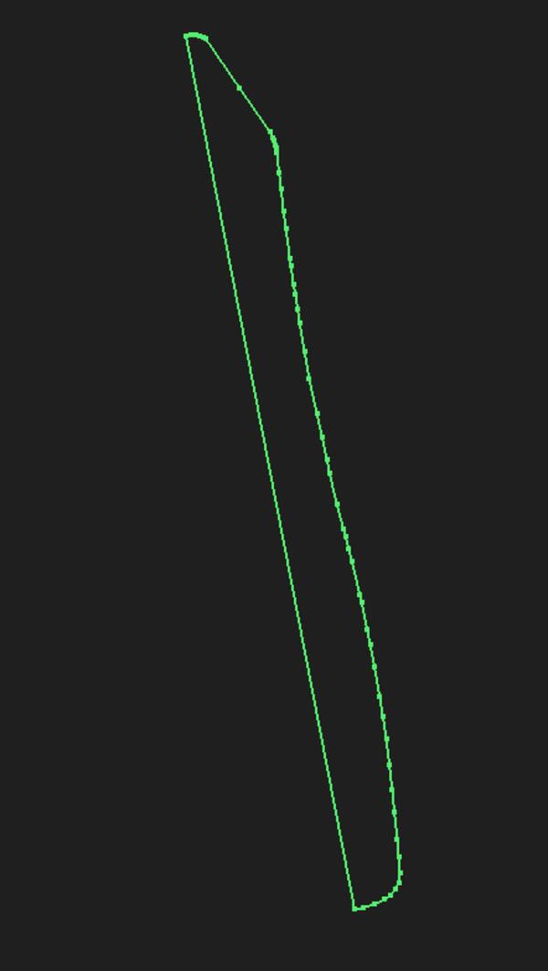
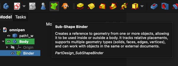
I use shape binder to make an outline based on the svg-shape.
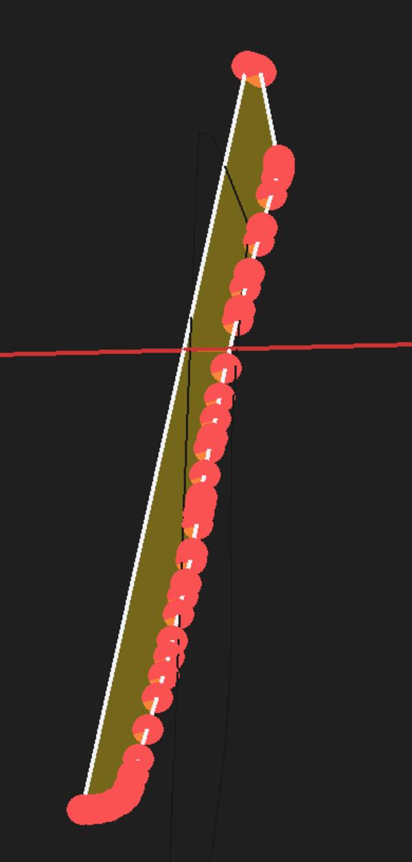
Then I select Revolve and select Select Reference and click on the long side of the shape.
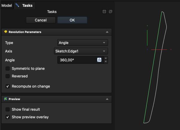
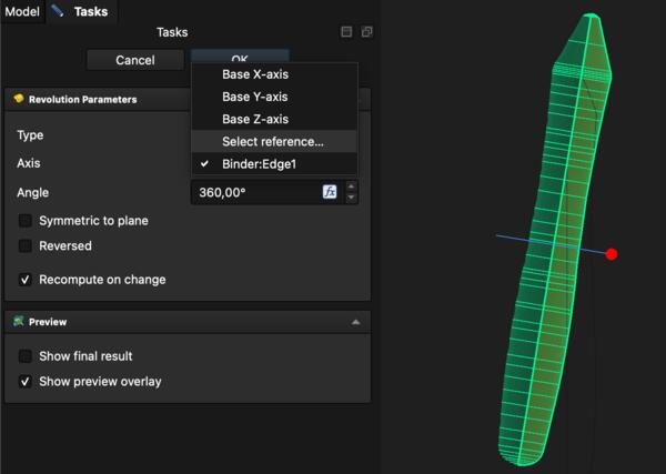
Now I have a 3D shape of the pen.
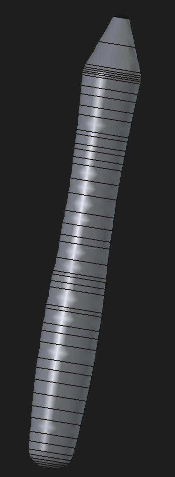
I soon realize that I cannot really adjust the parameters of this shape, So I return to the shape binder and sketch new shape based on the binder. I constrain the distances of different points from the long side and also the distances of each adjacent point. I don’t have the pen with me now so I don’t have the exact length but it can be easily adjusted later.
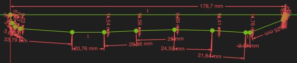
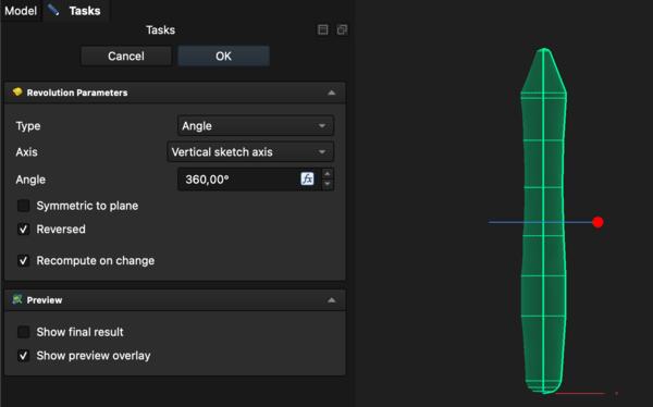
I also constrain the top end to the origin and revolve a 3D shape of the sketch when it’s fully constrained.
But now I want to make this parametric so I create a spreadsheet in which I place variable for pen’ outer thickness and length. For now the value is 1 as acts as multiplier for the dimensions defined based on the shape. I create another parameter for inner size, i.e. the hollow area that encloses the electronics.
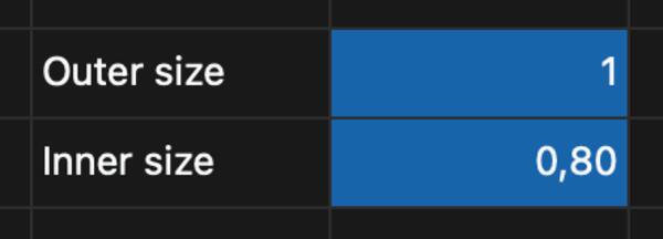
Then I place the “outer”-parameter to each dimension defined in the sketch as a multiplier. This way, when I adjust the parameter, it impacts all the dimensions equally.
I go back to the sketch and add the variable to each dimension.
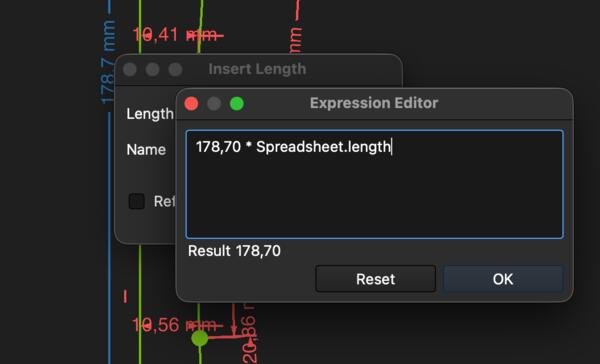
Then I take a copy of the PenShape body and in its sketch I change the dimension multiplier to the inner size. Except the tip area stays the same: 1.8mm in the inner and 2.8 on the outer sizes.
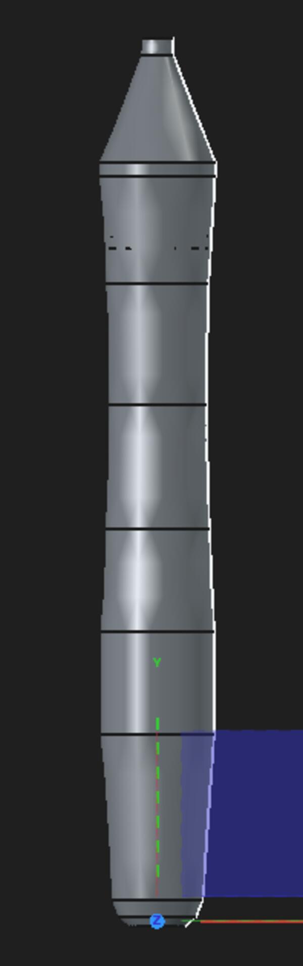
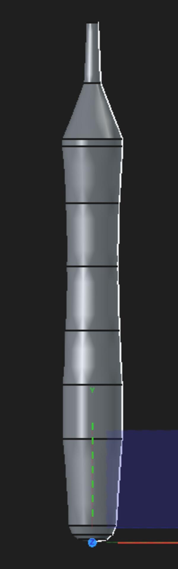
I use boolean cut in Part workbench to make the copies of these two bodies into one hollow shape.
Designing the pen shape for the electronics
On KiCad, I made the PCB a bit shorter.
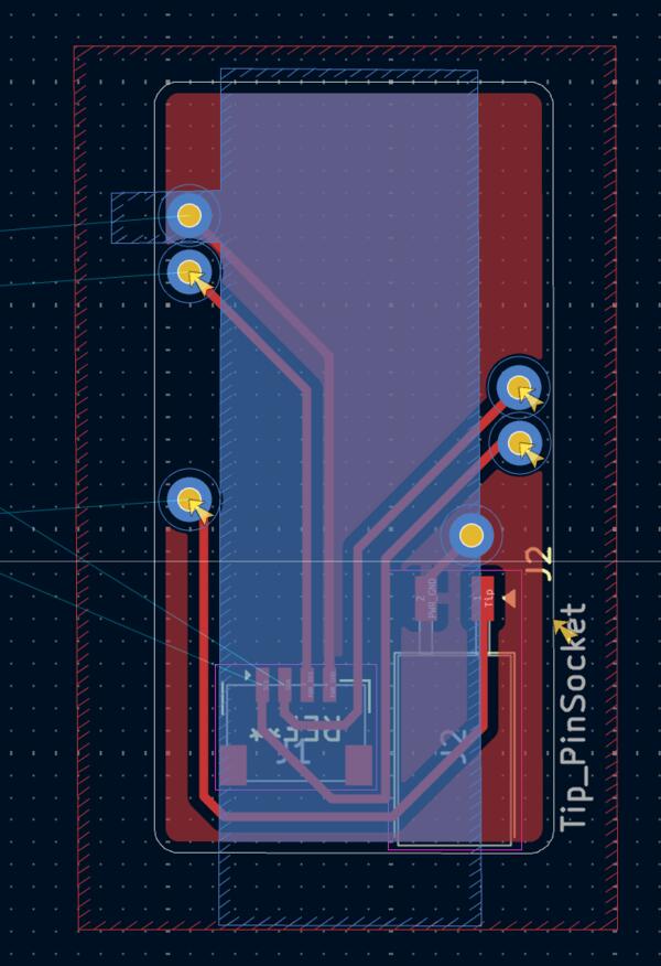
Then I exported the 3D model as a STEP-file and exported it to FreeCAD. I rotated and positioned inside the pen to see how it fits and it looks quite ok.
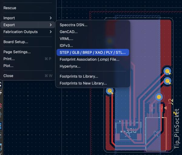
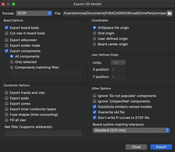
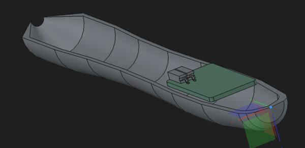
I go to KiCad to make the other PCB. It has one connector for the tip sensor button and then Adafruit IMU double-taped on the other side and that has integrated STEMMA QT connector. So basically this PCB is the size of the Adafruit board (1inch x 0.7inch = 25.4mm x 17.8mm) with one 2 pin socket. I’m going to route the connector so that pressing the tip sensor button connects the routes.
The schematic looks like this.

Layout looks like this. It is the simplest PCB I've made this far.
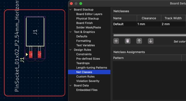
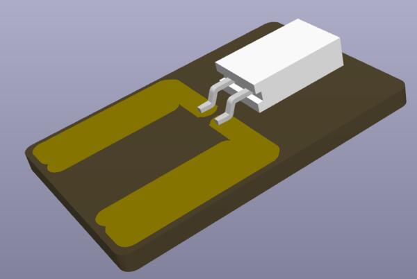
Later I decided to add an actual button to the board to have more reliable.
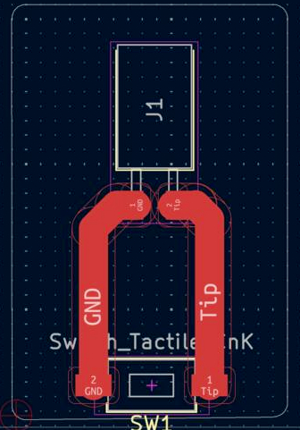
I export the boards from KiCad as STEP files, import to FreeCAD and position them accurately.
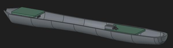
Now thinking about how to make the boards stay in place inside the case. The XIAO and IMU are not visible on the 3D view. I decide to make the boards 2mm wider and longer so that I can have a support structures for the PCB board without them touching the XIAO/IMU. Now, the Fill zone as GND reaches the GND pin without the B.Cu so that a bit simpler to mill. So I remove the extra via for GND.
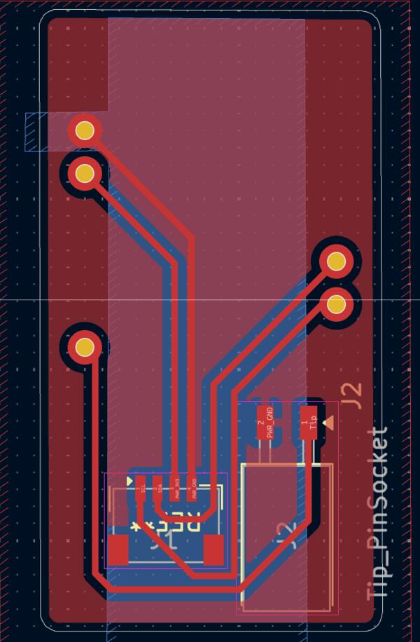
After exporting it to FreeCAD, I decide to only widen the board, not lengthen it, so that it would fit better.
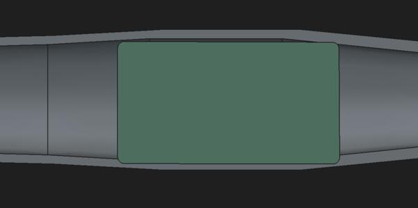
It is still a bit too large, but I decide to make the pen a bit wider instead. Then I decide to make the casing thicker so that it will support the boards.

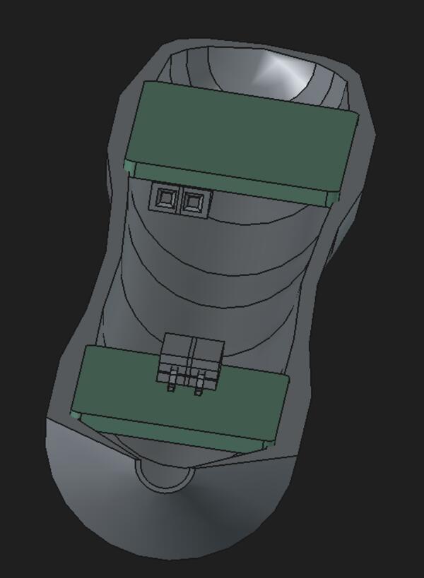
Now I continue to make the tip sensor button and create a 2mm thick cylinder and move it to its place.
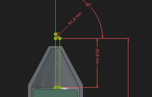
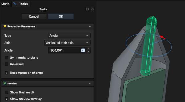
I used two copies if the Tip, made their radius 0.2mm wider, and used boolean cut to expand the hole for the tip.
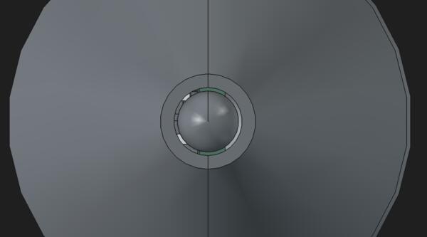
The spring for the tip sensor button is 7mm in dimaeter and 12mm long. In the reference pen, the tip comes 5mm out of the pen. Based on those parts, it would be good to have 1mm press for the button to activate.
I made a quick sketch that shows the size of the spring.
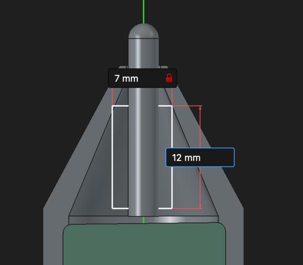
Overall, I used boolean operations (cut and union) to make the pieces as they are.
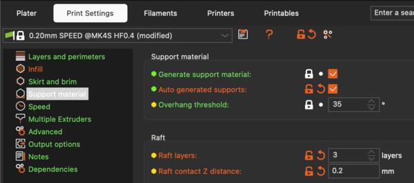
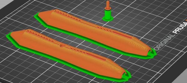
The pen tip is 3.6mm wide and it is not probably successful if 3D printed as such but needs some type of support system. I hope to get some help from PrusaSlicer for that.
Here's some further advancements I made for the tip and I think it's just better to let the videos explain them.
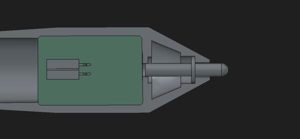
Now I’m thinking on how to make the two sides attach together. I ask Kris for an opinion and he suggests using bolts with heated inserts. The diameter of the insert is 3.9mm and I need to model a hole of that size in which I heat the piece in and on the other side a hole for the bolt. The bolt dimensions are 12.8mm lenght, 2.8mm diameter, and 5.6mm cap diameter. Pen’s diameter in the narrowest point is 19.78mm
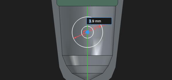
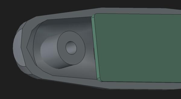
I made cylinder for the heated insert and also a bottom part that makes it fit the round shape of the pen. Then I copy pasted it and moved the copy to the second place. I needed to boolean union all of the three at once for the union to work properly.
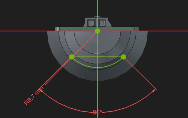
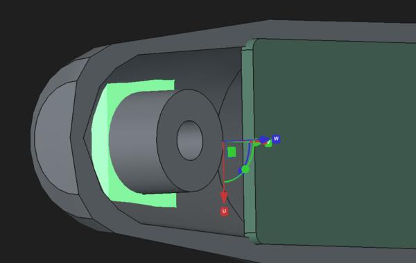
I copy pasted the pen shape with the heated insert holes and rotated it 180 degrees on Y-axis to make a fitting top piece with the bolt holes.
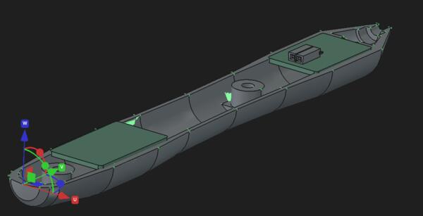
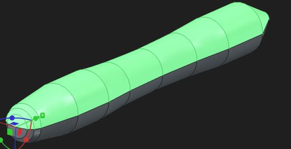
So I make 3mm holes for the caps of the bolts to become embedded in the pen.
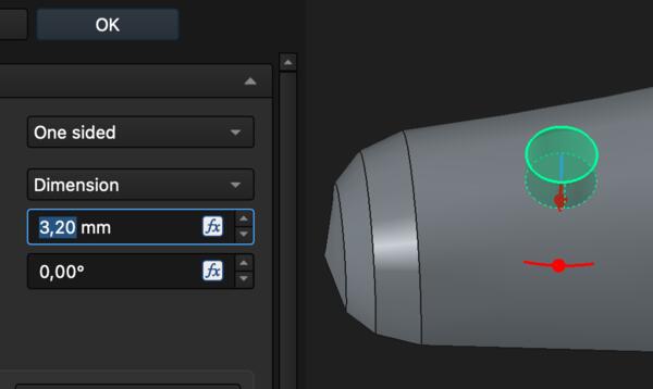
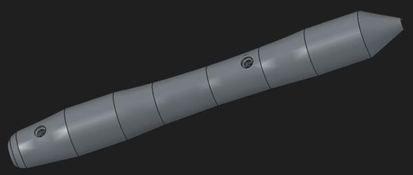
Then the last thing is to cut the areas for the PCBs. It won’t seem to allow boolean operations with those imported PCBs so I make similar pads as the boards are. But the boolean cut does not work with a simple pad body either and I have no idea what is the problem. Eventually after trying enough, I found that I needed to de-union the bottom piece because FreeCAD didn’t allow any boolean operations for the outer area after the holes for the bolts were unioned.
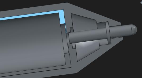
I had totally forgotten the scaling of the measures when was the time for that and of course it’s not working anymore when all the small parts have been done. This is an example how a bad practice blows back.
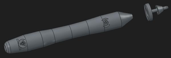
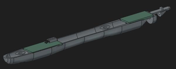
I fix the original sketch of the outer shape by placing the scaling parameter to 0.8 and adding more thickness to the pen in places where the boards need to fit. This was surprisingly straight-forward. Now the pen is 15cm long.
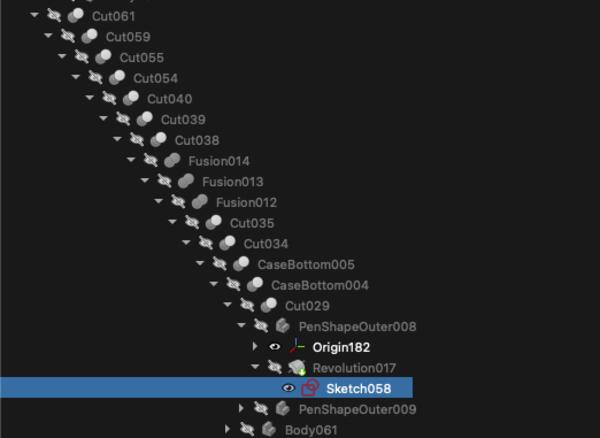
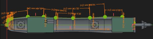
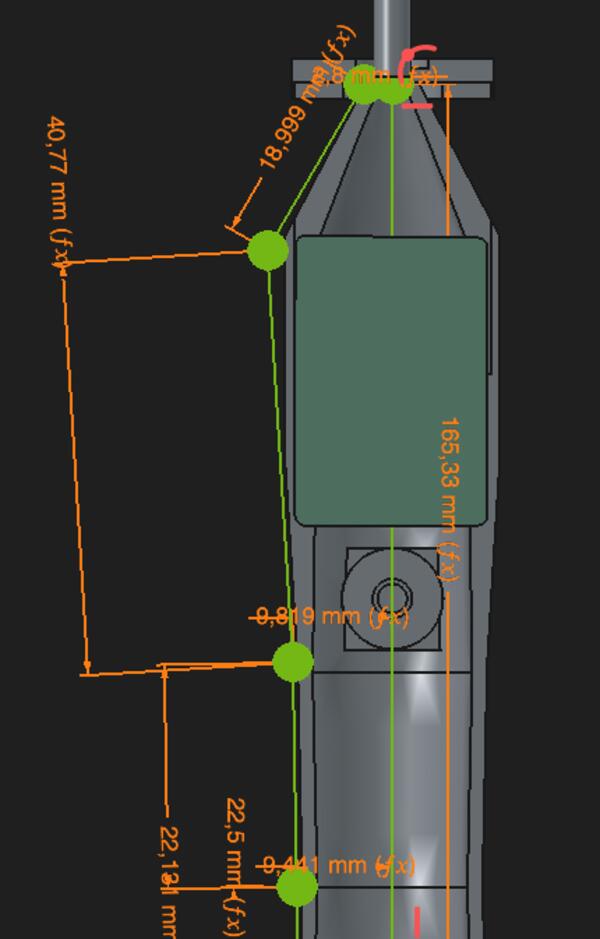
I remove one heated insert hole and move the other to the center and then make a hole for the USB cable
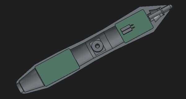
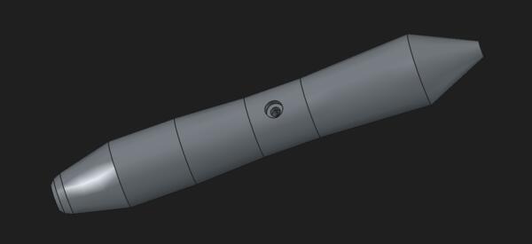
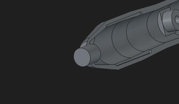
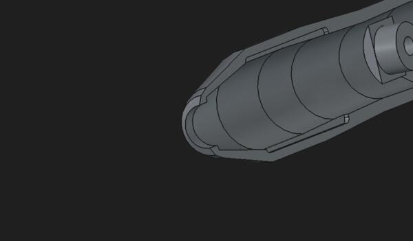
I continued to slicing where I added some more supports due to the tip-piece but it was somewhat of an overkill.
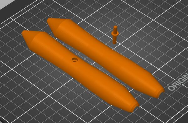
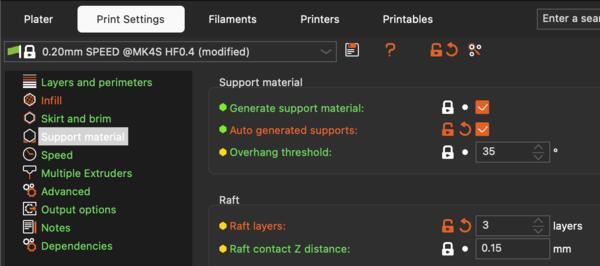
PCB production
During the printing I began milling the PCBs on Bungard. I did this almost from my memory (double-checked from aalto wiki) and I didn't take any screenshots of the process. Only a couple of videos.
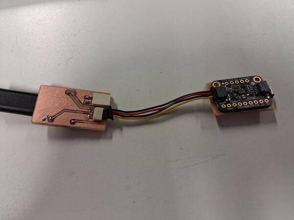
While waiting for the 3D print to finish, I glued and soldered a button to the side of the IMU PCB so that the tip presses the button when writing. The first cut was too deep and for the second I added the depth limiter.
Then I soldered the components to the boards and then it looked like this:
After printing was done I realized that the USB is way larger at that point than only the wire. So I saw the top side.
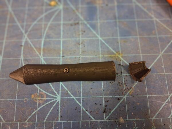
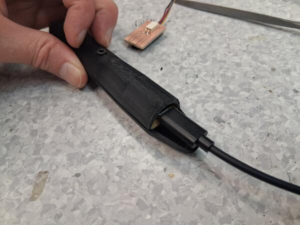
There was also an issue with the boards not fitting "at all" within their planned spots.
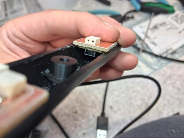
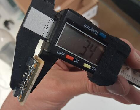
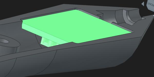
I increased the space fo the board and launched a new print for the top piece.
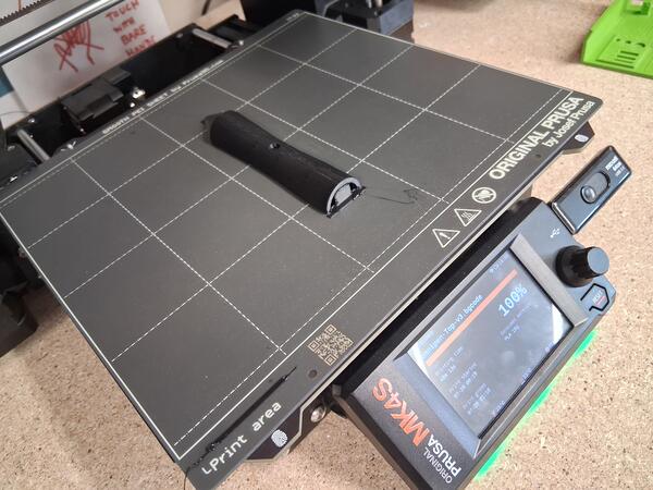
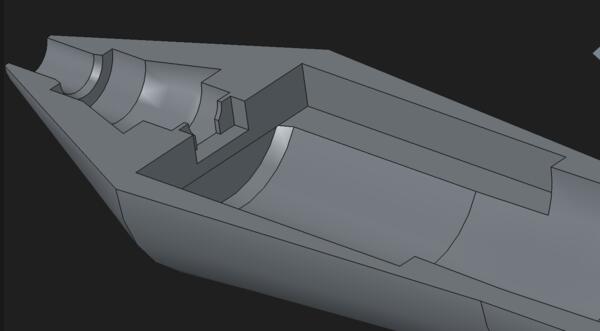
The pen tip was rather wobbly so I came up with a more integrated spring solution, in which the tip has an outer casing for the spring. This video also demonstrates my most common workflow (transforms and boolean operations) in the making of this 3D model.
The button is 2.5mm high, 3.65mm deep and 6.1mm wide. I update the 3D models to inhabit the button under the tip, and fix any small issues and print the new tip with the updated case-pieces.
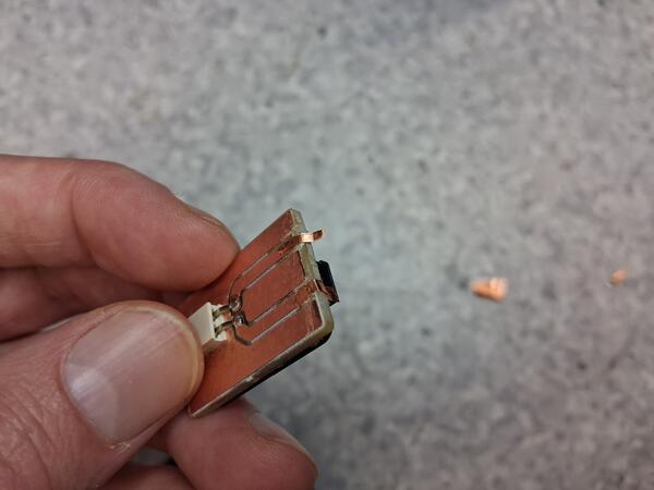
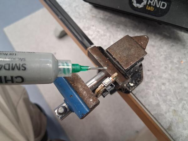
I add small slices of copper tape to have the button on the side of the board. Then I use this special soldering technique with a syringe (which name I don't remember now) as well as some glue to have the button in place connected.
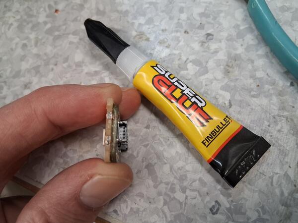
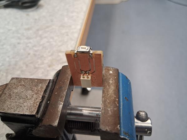
Now with the new prints, I have the pen assembled well enough to be tested.
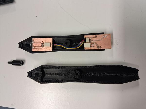
Programming the MCU
Now I continue to programming the microcontroller. To install CircuitPython on the nRF52480, I follow these instructions by Seedstudio. I download the firmware as instructed, double press RST on XIAO and drag the firmware to XIAO-SENSE.
I copied the example code from Adafruit’s learning material and saved it to the XIAO as main.py. I also find the LSM6DSOX-library from Adafruit’s library bundle and copy it to lib-folder on XIAO.
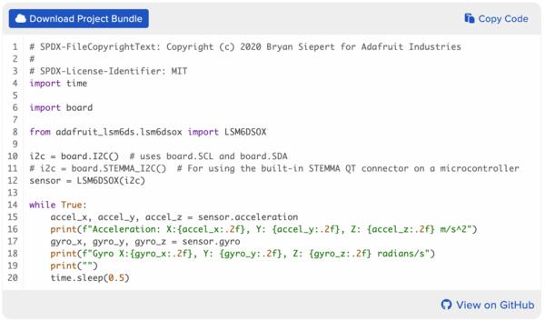
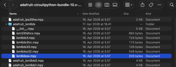
Trying out, I get this error: Incompatible .mpy file...

I asked Gemini what’s the problem and it was about having a different version of circuitpython installed on my computer than what the library depends on. I download the latest circuitpython from circuitpython website https://circuitpython.org/board/Seeed_XIAO_nRF52840_Sense/, put the XIAO on bootloader mode and drag the new uf2-file in XIAO-SENSE.


Trying again, I get the ImportError so I copy-paste also the adafruit-register -library from the bundle to the XIAO.

Next I get RuntimeError: No pull up found on SDA or SCL; check your wiring.

Only now I realize that I should have used the I2C pins, D4 and D5, but I use D3 and D4. I’ll try if I can make it work with these pins. Otherwise I need to mill and solder again.
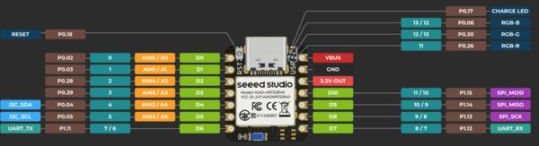
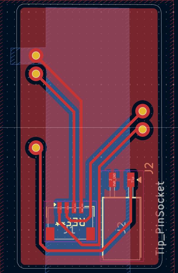
Now as I look the connector, I realize I cannot twist the STEMMA QT wires as they fit to the socket in only one way: I cannot make GND connect to GND and SCL to SCL, and they were connected in the opposite way. So I need to redesign the PCB for the XIAO again. This time I make sure that GND connects to GND and that I use SCL and SDA pins correctly.
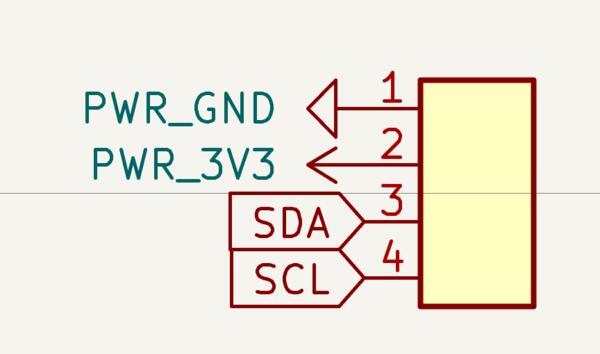
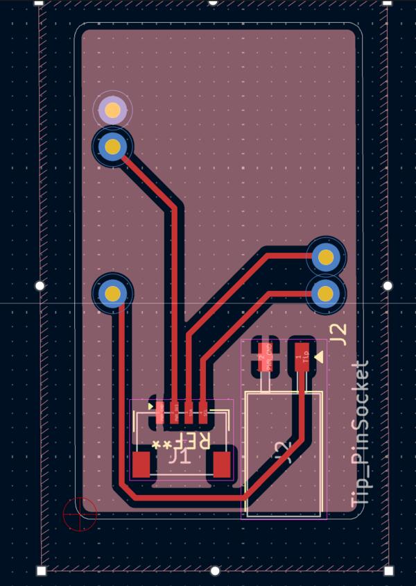
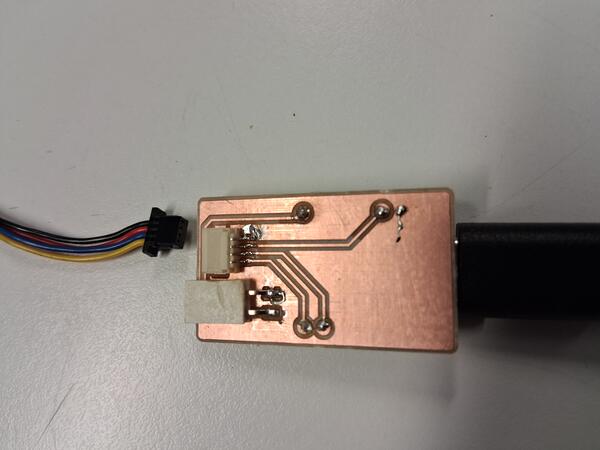
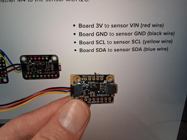
Suddenly none of my USB devices wont work when I plug the XIAO in. I wonder if there was a short circuit somewhere or if the board has broken all together when I desoldered it from the previous PCB. There are no lights on. But when I disconnected the Adafruit board, the light on XIAO went on.
And I found the critical issue: on XIAO I have wrong pins also on GND and 3V. I moved both of them down on KiCad and milled and soldered a new board.
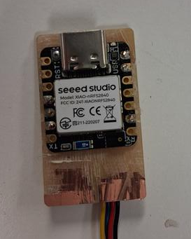
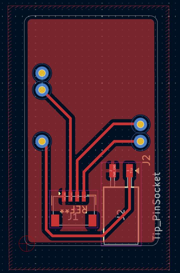
Now I began to have a lot of trouble desoldering the XIAO board as the solder wouldn't come out of the pin holes. After a while of trying out with solder iron, hot air gun and a lot of solder resin, I wasn't able to stick a wire through the hole, but instead burned the XIAO board. It was the only nRF52480 XIAO that I had. Luckily one of my classmates was willing to give his so I was able to continue with it.
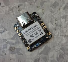
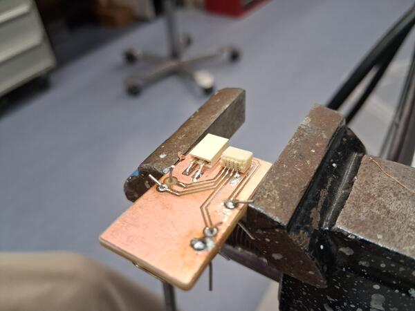
With a new XIAO board, it took only a moment to get everything in place. Only aesthetic issue the botton piece became printed a bit wonky.
Now trying to test the button, I only get value True.
Testing with multimeter, I find that the button solderings are not connected. I thought that maybe the copper tape is insulated on the bottom but that was not the case. I add solder to the button and got it working.
Here's a video of rest of the assembly.
The button was, however, not working anymore. It had probably taken some damage during the assembly.
I get correct data out with the Adafruit's example code, but at least with this type of presentation of the IMU data, I cannot find any meaningful patterns when moving the pen on one axis or the other.
I let the button be nonfunctional for now, and continue to developing the code.
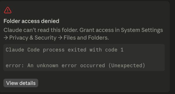
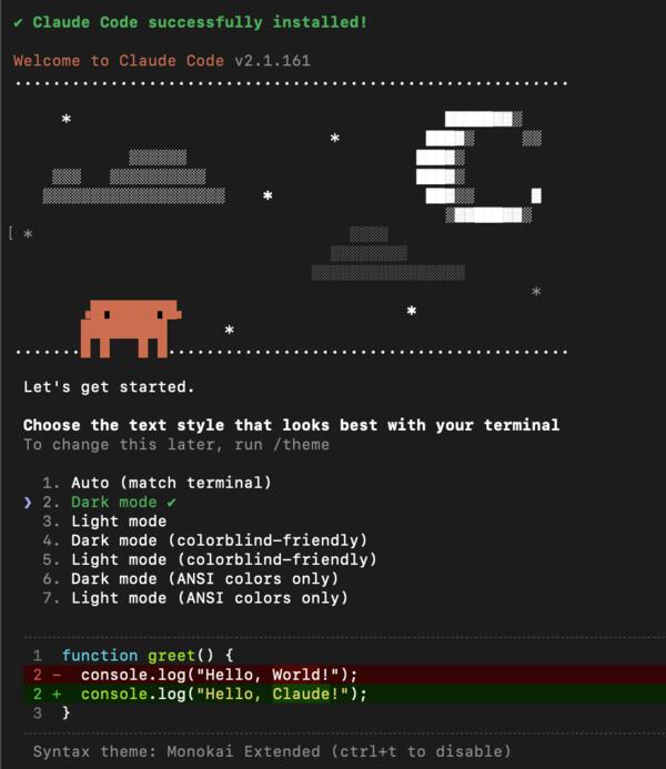
As I have only about a day left until I have to present something. I went to Claude Code (I have the cheapest paid version of it) to get some quick help. Claude desktop version couldn’t get access to my folders (due to apparently common MacOS sandboxing problem) so I install the command line (CLI) version, as instructed by Claude Chat.

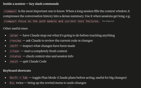
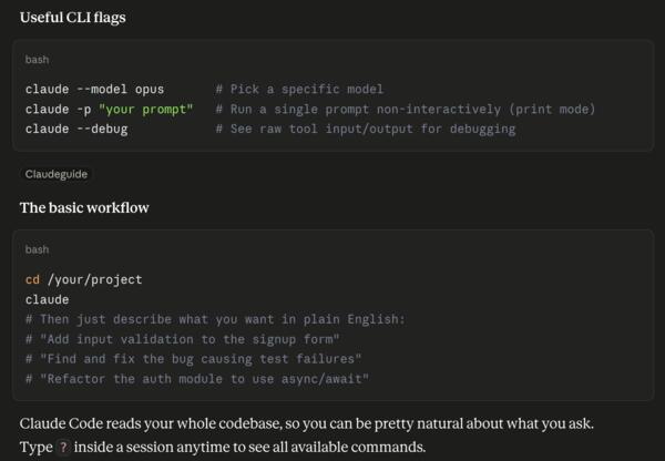
I also ask it to tell me how to use it.
Claude Code
The prompt that I begin with is the following:
I'm making a "pen" with XIAO nRF52840 Sense and Adafruit's LSM6DSOXTR that can recognize letters/patterns written with the pen and saves them as text. I have the hardware ready and have the XIAO reading the gyroscope and acceleration data from LSM6DSOXTR. I have thought of using EMNIST database for teaching letter recognition. Can you write me the code with beginner-friendly documentation explaining the code that does the training as well as the code that recognizes the letters?
Claude prepared the files for training and running the pen and provided me with the following instructions.
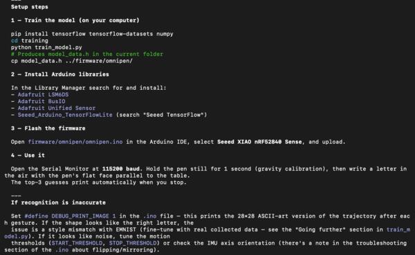
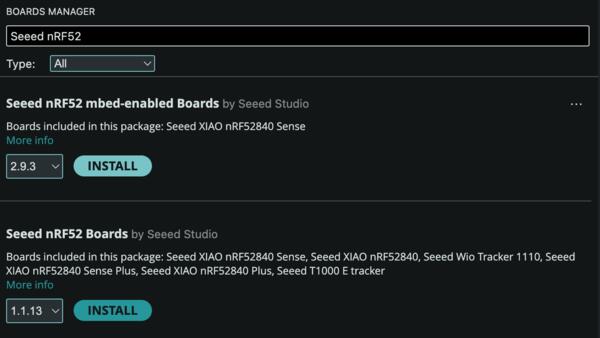
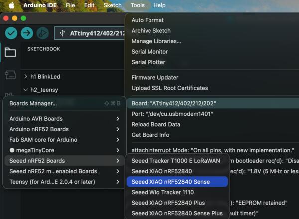
I further clarified that I'm planning to use CircuitPython rather than Arduino (which I have less experience with) and that the pen needs to recognize letters written only on a surface, not air. Apparently the (used) machine libraries for nRF52480 were only for Arduino so that needed to be used. I added board manager for nRF52480 in Arduino IDE and selected it for use.
Trying to run training_model.py, I get an error, which Claude explains to be a hardware architecture problem: the installed python was for intel processor while I'm using apple silicon. Claude instructed to use a virtual environment for the installations and training.
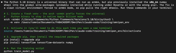
Now I was able to run the training model. Continuing to the next steps of installing the libraries.
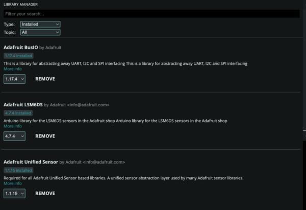
But I couldn't find the last, tensorflow-library on Arduino IDE Library Manager.
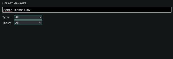
Claude proposes two options and I try out the option A.

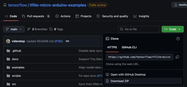
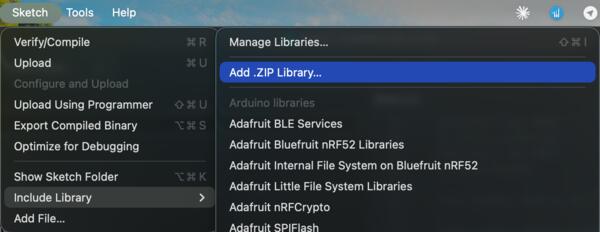
After the .ZIP-install I get again error that that Claude translates into two different problems: the TensorFlow-library was deprecated and that I hadn't ran the training again after the recent changes were made. Claude claims that the library was wrong and I need to install the correct and latest one, but I was sure that the library was exactly what it expected and there wasn't any other to be found on GitHub. We did a few prompting rounds of trying to make the library work, all the time Claude editing the files and me replacing the old files and rerunning the training model (which takes around 5 minutes).
Finally Claude declares that the library is incompatible with the XIAO board and we should use the EloquentTinyML library instead.

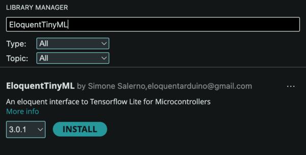
So I install EloquentTinyML library which happened effortlessly. I should have done it already in the beginning when Claude recommended it.
Then I install the library that apparently is mostly used in EloquentTinyML. Claude states: "EloquentTinyML v3 is just the API wrapper; this is the actual TFLite Micro engine it calls into".
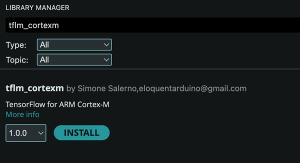
Now the library began working but I get an even more cryptic error expressing something about a RingBufferN. Claude removes the whole template as "We never call any of it. The RingBufferN<> template it uses only exists in the Arduino mbed core, not in the Seeed core."
Running again I get a page long error message, and the Claude gives up and says that the way forward is to leave all library dependencies and instead write all the code in C++ instead.
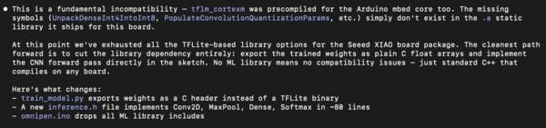
To me this sounds quite impressive and ambitious and I tell Claude to go for it. It does its thing and eventually provides me with the following instructions:
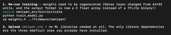
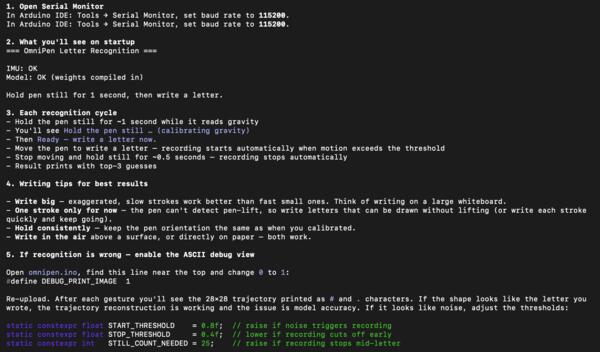
Now there are no errors and I continue to testing the pen.
The program didn't recognize the letters and it's getting late so I call it a day.
I had left my meatballs in the room temperature for 8 hours but being hungry I had eaten them anyway and in the night and morning I became sick in stomach. Because of this, I didn't have enough time or energy to continue fixing the pen the next day, and I needed to proceed making the video of the process to be presented to the class. Now rereading all the instructions, I realize that Claude gave further instructions on how to adjust the sensor reading and it could have been an easy issue to have the pen working much better for the presentation.