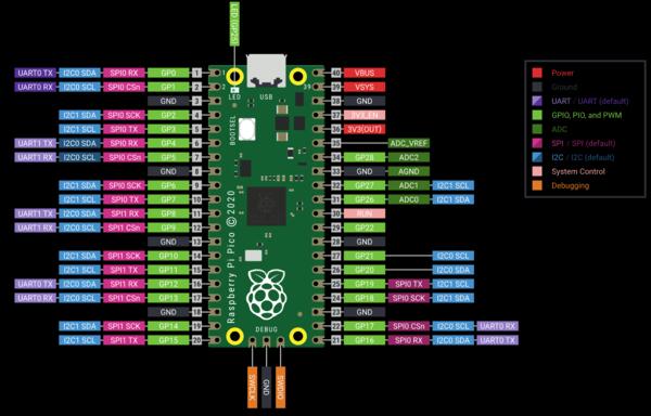
Week 06: Electronics Design
The main outcome for the week
I simulated a LED blinking button push reaction game with Wokwi:
Then I designed a custom PCB for creating the game:
Design files made in these week are available at my gitlab repository
Test Equipment for a Microcontroller
Logic Analyzer
Logic analyzers are tools for analyzing how specific communication channel looks like in electronic signals: i.e. I2C between XIAO and OLED screen. They allow connecting multiple leads (data points) on a circuit and stores the data for analysis on what’s happening on a signal level. This way we can identify and locate communication issues, debug, and just check whether signals match the expected behaviour.
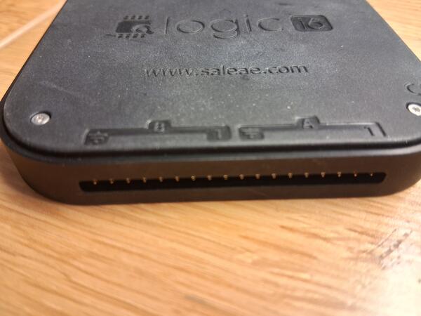
These are the equipment available in our lab: Saleae Logic Pro 8 (datasheet), which Kris used for demonstrating, and an older one Saleae Logic 16, which I used for learning to do the same process myself. On the devices are visible the channel numbers and ground pins (all the pins in Logic Pro 6).

We were analyzing the communication (and connection) between XIAO RP2040 and the OLED screen which soldered in embedded programming week
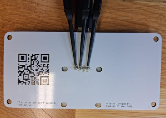
So the black wire on the left is the ground and then I used two wires on the right, i.e. channel 0 and channel 1. The wires were plugged in the clips like that.
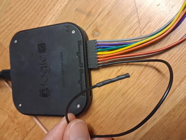
On the screen are the labels which pin is which. Alternatively the clips could be attached to the
microcontroller's corresponding SDA, SCL,
and GND pins (SCL Serial CLock and SDA, Serial Data).
Here the black ground wire
is attached to the GND pin on the screen.
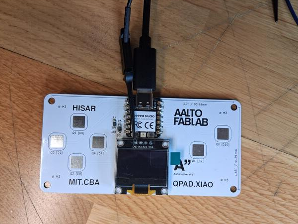
I had some trouble attaching the clips in their place in the pins as they we're snapping out all the time. The soldering was quite extensive and cone-shaped on both sides of the board, so we ended up taping them in their place (which I apparently didn't take a photo of, imagine tapes on top of the clips on the image below). This testing phase could be made easier and taken into account already in the soldering phase by trying to leave a spot for these type of clips to bite. Even soldering a temporary short copper wire is an option while it might slightly interfere the signal.
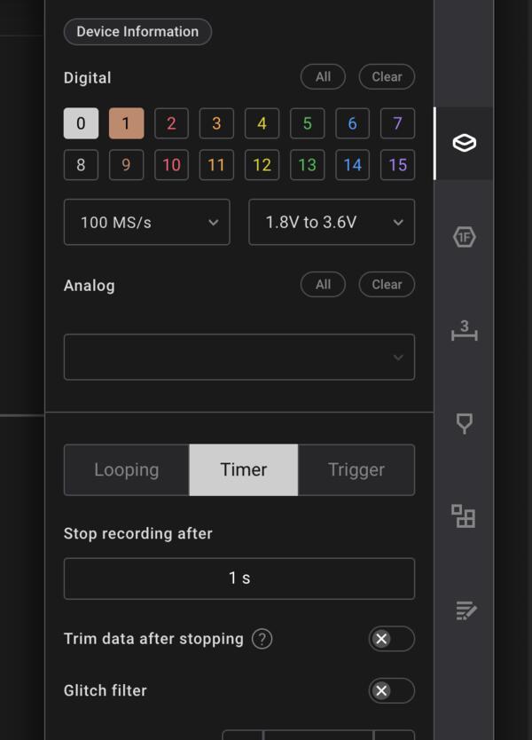
I downloaded the Logic software. Here is an image of the settings we selected on the software before running the analysis: channels 0 and 1 (the connected wires on the device), the rate to the fastest one 100MS/s (million samples in second), voltage to 1.8V to 3.6V (XIAO RP2040 runs on 3.3V), and timer to 1 s.
I had at first connected a wrong wire: the third one instead of the second one (they were so close to each other!). This, on the other hand, demonstrated what it looks like also when there is a problem in the circuit (or connection like in this case): the analyzer shows nothing. The second video shows the successful run as we got the correct clips to stay in their place.
I can't say I really understood what is all the information one can gain from this type of analysis, except that if nothing is showing, then there are problems.
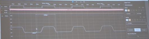
Logic Pro 8 measures also analogue signals (at rate of 12.5 MS/s) and below is demonstrated the difference between digital (upper) and analogue (lower): analogue voltage shifts more slowly as digital is basically either on or off / 0 or 1.
Oscilloscope
Oscilloscope is somewhat similar to Logic Analyzer. It measures voltage in a high rate. You can test if it works by using the pins on the oscilloscope. Other pin needs to always be connected on the ground.
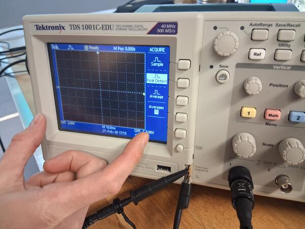
You can use the lower knobs to zoom in and out (scaled) the image vertically and horizontally. The upper knob on the left is a multiuse knob for navigating the menus. The arrow on top tells when the the wave moves up and can be set to point the falling as well. In measure menu there are multiple types of measurement
Hz (hertz) in an unit of how many waves per second. Pk-Pk (peak-to-peak) refers to a difference between the highest value and the lowest value.
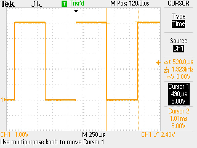
For some reason I didn't take many photos for documentation when testing this device as it's use seemed quite simple. Again difficulties arise if I need to interpret the waves for debuggin or other. Below is the image we saved from the oscilloscope on a flash drive.
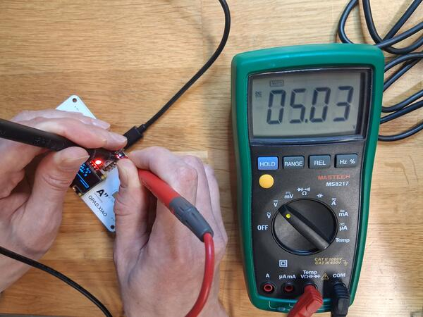
Multimeter
As I'm running short on time, I won't go through in precision all the things we tested with multimeter. It can be used to test many things: AC/DC voltage, AC/DC current, resistance, capacitance, LED polarity (diodes) etc. AC is symboled with ... (three dots) and DC ~ above the letter. You don't need current in your device to test connections, it is provided by the multimeter. The multimeter in our lab has a quite approachable user manual for quick reference.
Below is an example where we tested the voltage of the two power pins on XIAO RP2040.
Few words on my learnings
It is rather difficult to specify what I have learned as everything has again been so new to me. My understanding of electricity and electronics and the main concepts with them has definitely widened and come more into practice. I have been quite tired and exhausted this week while having many other duties so reflecting on my learnings doesn't come too easy right now.
Electronics Design: KiCad
I began by downloading KiCad and installed it without the default library table by selecting "Create an empty global symbol library", and chose the same option for footprint library. Instead, I installed KiCad FabLib, which has already compiled the components that are used in Fablabs. This was done in Plugin and Content Manager -> Libraries tab -> Search "KiCad FabLib" -> Install
Then I was ready to create a new project, which resulted in two files: the schematic (_sch) and layout (_pcb) files for two different editors. On the right there are the editors/tools available in KiCad. I started with schematic editor (double-clicking the file). The basic editor settings are on the left, where one can configure measure units, grid (also right click -> Grid), cursor and settings for routes. On the top toolbar on right are the main menus for circuit design:
- Symbol library editor for finding symbols (that might be missing)
- Footprint editor for adding a footprint
- Annotate Schematic... adds identifiers to component symbols
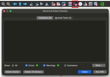
- Electrical Rules Checker: check if connections are correct and working
- We did not cover Simulation or Assign footprint (as installed plugin adds right footprints automatically)
- Bill of materials lists the parts (and their information) needed for the project based on the symbols on the schematic
- PCB editor is where the board layout is designed (based on the done schematic)
Also worth mentioning here are the layers on the right, similar to many visual design software, which refer to different physical layer on the board. The main quick keys are
- S to select items,
- A to place symbols,
- P to place power symbols,
- R to rotate them, and
- W to place wiring in schematic view and
- X in PCB view
- G to grab connected items.
Dragging from left I can select only items that are fully covered with the selection area and dragging from right I select all items that are overlapping with the selection area. There is also unwritten convention that power symbols go to the top, grounds are placed to the bottom, inputs are on the left, outputs are on the right of the schematic, so I follow that.
Schematic Editor
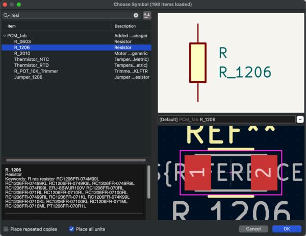
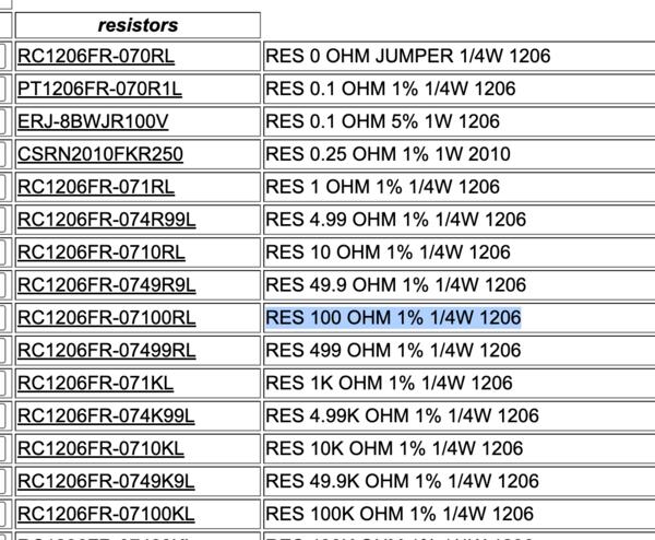
On the right are the tools used for creating the schematic. The main one is the Symbol placement (A), which opens a menu for choosing parts which have been defined in the installed library. The filter/search can be used to search items which I use to find and select one resistor to begin with: R_1206 and then place it on the board. The number after R_, in this case 1026, is the physical size of the resistor. Each take a resistance value as a variable. The small resistor has an upper limit, though, which has to be taken into account. For the middle size can likely be assigned the necessary resistance that is used in our applications now. The upper text next to the placed symbol is the unique identifier for the part and for the lower text I write the used resistance by double-clicking it with selection tool. I should to use those resistors/resistances that are available in fab lab inventory.
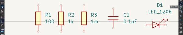
I also select one LED of a same size (LED_1206) from the symbol menu, and from the Power symbol placement tool (P). place power symbols for 3.3V input (the voltage for RP2024 for example (and possibly other microcontrollers as well?)) and for ground. Power sources and grounds need to to be flagged with a PWR_FLAGs. Also, to have power input and ground visible in the PCB layout, I also place a connector for which I connect same symbols with same identifiers and KiCad recognizes them as references to the same symbols. Now I have one really simple circuit.
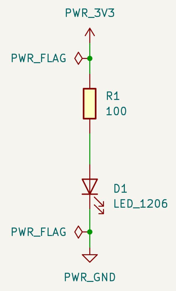
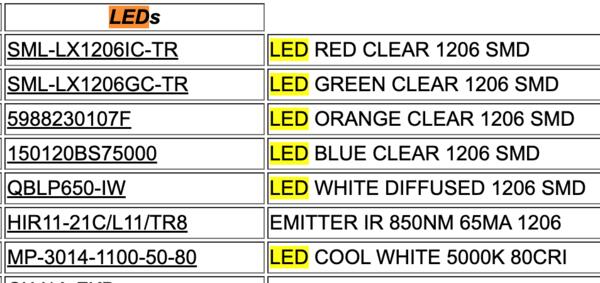
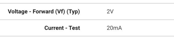
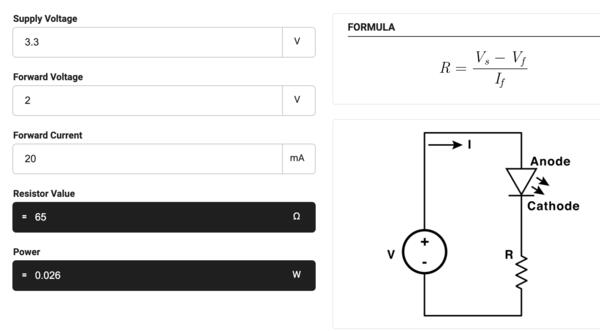
The LED (orange in this case) needs a resistor of a right resistance to prevent it heating up and demanding more voltage and ultimately breaking down. Different color LEDs have specific voltage needs. The right resistance is calculated for example with KiCad LED Series Resistor Calculator, and where voltage is 3.3V (from microcontroller) and current is checked from the LED’s datasheet (go to FabLab inventory (), click the correct LED code, look for forward voltage and current, if not found, open datasheet, and find them there). The orange LED has forward voltage of 2V and current of 20mA which leads to a need for 65 ohms resistance. In. the inventory there are 45 and 100 ohm resistors and I choose 100 ohm resistor to play it more safe than bright.
Going forward, I don't actually need to have the power supply placed because that is provided by the microcontroller (they were only presented to demonstrate how to deal with them). So I remove the power in and the connector and place the microcontroller for which I choose the generic XIAO board so the most adequate model can be flexibly decided later. Microcontroller is the central component (in regards to intelligence) so it's commonly placed to the center of schematic. I place the Power in (PWR_3V3) symbol to the microcontroller's 3V3 pin and connect the resistor and led wiring chain to the pin D0. I also ground the microcontroller and place No Connect Flags (Q) to the pins that are not used.
At this point I run ERC (electrical rules check) to see if there are any problems, which there are none at this point (perhaps because I'm following Kris's tutorial :)). It's good to run ERC at least always when switching to PCB Editor.
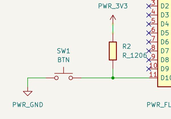
I continue by adding a button to the circuit. Press A to place symbol and search for button, I select the Omron Push button and name it BTN. Without the microcontroller's built-in pull up resistor, there should be made one by placing power source and a (10k ohm) resistor in junction between the pin and the button (as demonstrated in the image below). The pull up resistor is to have a minimal current coming in the pin and it is set to 1 or HIGH, but as the button is pushed it is set to 0 or LOW. Without the pull up resistor the pin wouldn't be able recognize a stable state when button is not pressed, as it is not connected anywhere, but it would still be trying to sense HIGH and LOW state from static electricity variance around the pin. With the pull up resistor the pin remains connected whether button is pressed or not, thus providing stable, really small, current (reason to choose a strong resistor).
For the microcontroller, the pull up resistor for the specific pin need to be designated in the code with Pin.PULL_UP -parameter, as demonstrated in Microython documentation.
Input devices should I2C connection (inter circuit connection) and for that capability I need to check which pins on the board offer that quality. Clicking on the microcontroller I can find a link to its datasheet, where the pin functions can be checked. For example, for RP2040 which I used on QPAD the pins are D4 and D5, which I then label on the schematic (Place Global Label on the tool panel).
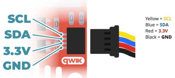
Then we use Qwiic connector which can be found in the library by searching JST_SH_01x04. It has specific wires for specific pins which are labeled in the schematic accordingly. Now this connector can be used for connecting a input device to the board.
Then I also to add a motor that can be controlled by the microcontroller. I add a pinsocket with three connections, in which the motor can be plugged in, and add 5V power symbol and ground symbol (every subsystem need to be grounded). I also add a 5V power supply to the microcontroller add power flag to it.

PCB Editor
The the green button in top right corner switches the view to PCB layout editor and there's another button for updating the PCB from schematic to this view (which needs to be clicked every time there's a change made in the schematic). By clicking that button I can place the used components on the view, which can then be connected with routes (X). It's probably good idea to move the components around to fit the wiring well. There can be no crossings of wires, except if you have two sided board, pressing V when wiring makes a via to another side. Pressing F autoconnects the wiring to it's destination based on the rats nest. Placing the components wisely on the board probably need some trial and error. As there's probably need for rerouting anyway, selecting one part of a route and pressing U selects the whole route, which can the be deleted as a whole.
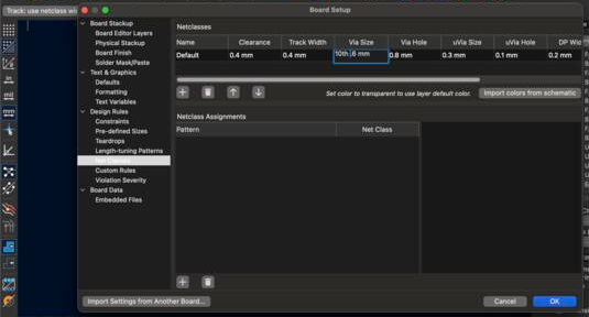
One important thing to keep in mind here is the width of the routes and the clearing between them for avoiding cross-talking. Those can be set from top left corner Track: use net class width -> Edit Predefined sizes... -> Net classes. For now I'm setting the Clearance for 0.4mm and Track width also to 0.4mm which are proper good quality values for the milling machine in the lab. The Via size 1.6mm and Via hole 8mm are also set to the lab default values. (The other values are not relevant at this point.)
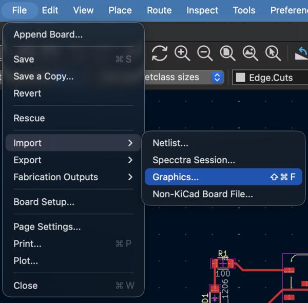
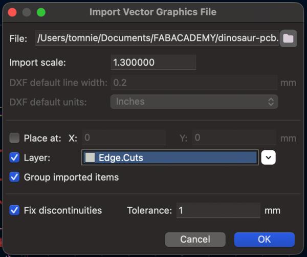
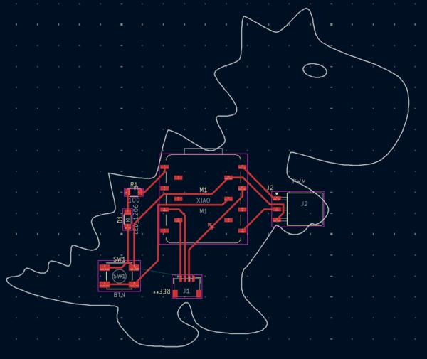
To make the outline for the PCB I select Edge-cuts layer and with the polygon tool define the outline for the board. The board can also be made into "any" shape with vector image. With Inkscape, I created a shape with connected strokes and export (save) it as .svg and import to KiCad on Edge.Cuts layer, select File -> Import -> Graphics... and then select the scale/size and for the layer select Edge.Cuts, and hit OK. This can be used for making creative PCBs just for fun or to make them fit and integrate in a specific product/creation (or both).


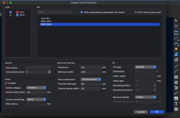
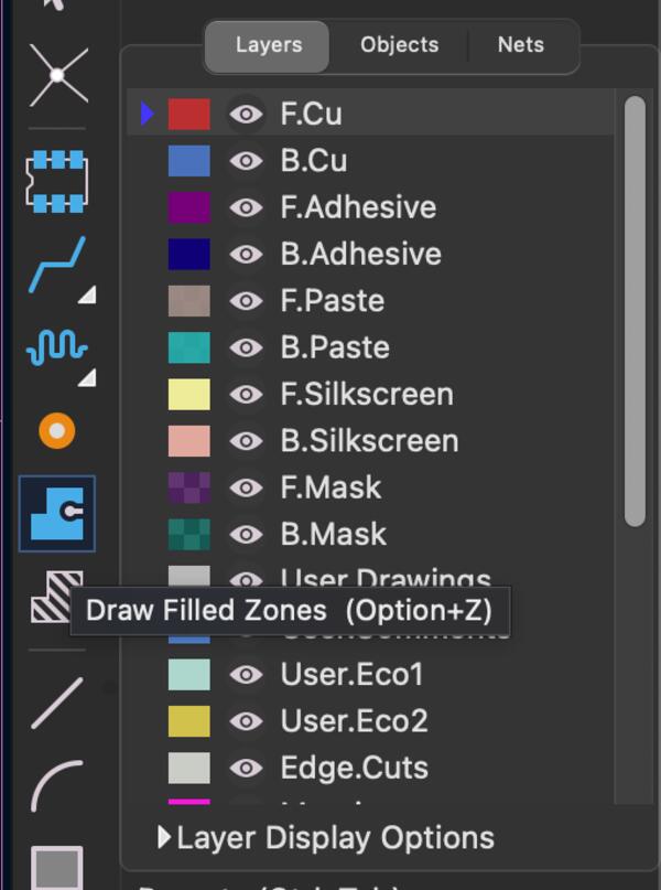
Filled zones are the copper area on the board where there are no wiring and shield the board connections from outside noise, signals, etc. Grounds can be connected directly into the filled zone instead routing it to a specific ground pin. For creating that there's a button on the right tool panel. On front copper layer (F.Cu), click on the background and for the Net select ground (usually). This leaves a clearance between all the other connections except the ground connections, and there's no actual need for routing the grounds. Default values for other fields are usually fine -> Ok. Draw an approximate area around the board, double-click when ready and press B. Now we don't actually need to connect grounds anywhere specific but just to the filled copper zone.
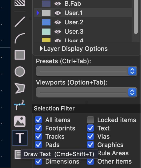
Adding text on the board can be done on Silkscreen layer, but for the production process in our lab we use User.Drawings or User.1 layer. I selected the User.1 layer and then select the Draw Text tool from the right side panel and write useful or not useful (whatever you want) information on the board. I can also import graphics on this layer in the same way as on Edge.Cuts layer.

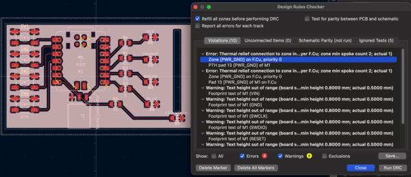
In PCB Editor there is Design Rules Checker similar to ERC in Schematic Editor, which is also used to check for inconsistencies in the design especially regarding the production of the board. When running DRC also the second tab, Unconnected items, require attention. There are arrows which point at the problems and selecting specific errors make the errors light up in the board. I should have checked and fixed these issues already before Filling Zones. Now removing connections leaves a gap in the copper zone.
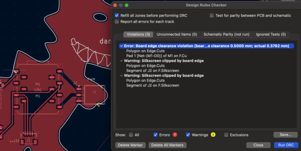
I removed all the wires moved the components slightly, wired and did the zone fills again. Now running DRC, I get a couple of warnings as the PWM is slightly over the outline which I'm ok to live with.
View -> 3D viewer. The model can be exported as STEP-file and import to FreeCad to be included in the wider 3D model.
Exporting to manufacturing
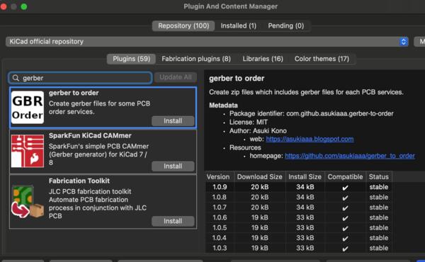
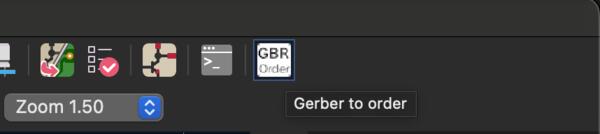
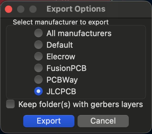
To export my board ready for manufacturing, I first go to Plugin and Content Manager and install gerber to order plugin. Then on the top panel I press Gerber to Order (or Tools -> External Plugins -> Gerber to Order) and select the manufacturer from the list, eg. JLCPCB or PCBWay. Clicking export I get a zip file. Going to jlcpcb.com (or pcbway.com) clicking order/quote now and upload the zip (gerber) file from the generated files.


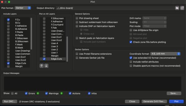
For exporting to PCB milling, I select Plot on the top left, unselect unnecessary layers and leave F.Cu and Edge.Cuts, and select Edge.Cuts on also on the next list of Plot on All Layers. Unselect also Indicate DNP, Check zone fills, Include netlist attributes, and Generate gerber job. Then select the folder and press Plot.
With Gerber view you can view that the board looks like it's supposed to.
Simulation
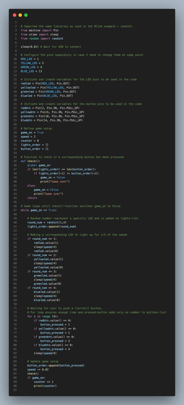
I began testing with simulation on Wokwi. I want to make a game that blinks lights randomly in an increasing speed and user needs to press right button for each light in the same order that the lights blink. When the user misses the order, all the lights start to blink for a while. Next iterations there can be sounds, screen for counting points, ranks, and a servo motor that spins when user misses a color.
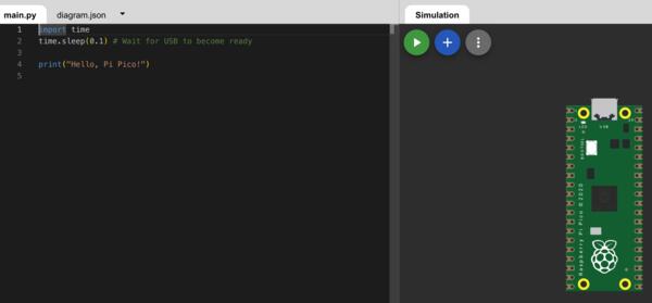
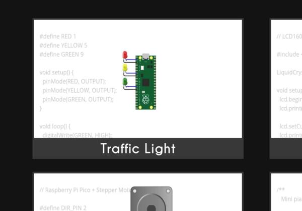
From Wokwi I selected Raspberry Pi Pico with Micropython starter template. To guide me with the code, I also opened the traffic light example to form the basis for the game as well as the Blink from Micropython templates.
Additionally, I opened a Raspberry Pi Pico documentation to check the pins.
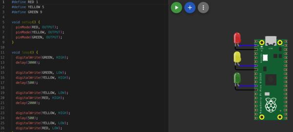
I began by defining the LED and Button variables in the code and adding the LEDs to the same pins as in traffic lights pins by clicking the + sign: Add a new part. The question mark above the part apparently leads to more information about the part, which is nice.
I began by writing code to make the LEDs blink as in traffic lights. At first the LED didn't blink although the code was running. Checking between the examples and mine, I realized I had connected the LED in reverse, as I remembered that the long leg is connected to ground, but apparently it is the other way around. Now the LEDs were blinking correctly.
Now I add buttons that light up each LED to test if the button inputs work and write the code for that. I also intiate the microcontroller's pull up resistors as third parameter, as in demoed in micropython documentation. I wasn't sure how the buttons are supposed to be connected to the pins so I checked it from the Mini Piano example. To figure out the state of the button to be used in the if-statements, I used print(redbtn.value()). I also added redled.value(0) and redled.value(1) to toggle the light. Repeated the same for all the colors. I have the buttons placed so that the wiring is more clear (I could also have used only one ground pin for all of the parts).
Now it's time to create the random generator and lists to check the correct order of lights vs buttons. First I add from random import randint in the beginning and created lists to be compared. I add randint in the beginning and add it to lights_order. Then I define a function check if lights and buttons have come in the same order. I reminded myself to the define the global variable with global when it's used inside functions. I solved to problem of giving time for the user to push the button with a for loop and adding only one time the button code in the list by defining a pressed_button variable. Now it seems to work well enough.
I also add the resistors to the LEDs which would be needed in real life for the LEDs not to blow up.
For each LED I check their forward voltage and current and calculate proper resistance using the KiCad
LED Series Resistor Calculator mentinoed before. In the inventory there doesn't
appear to be a yellow LED so I use the values from orange. They all have 20mA current and forward
voltage increases from red to blue.
Red and orange with 2V leds get 65 ohms, green 2.2V gets 55 ohms, and blue 3.2V gets 5 ohms.

I also want to add screen to show the counter. I chose Seven Segment Display (4 digits) because it appeared suitable. I clicked the question mark above the part and found this example done in micropython which I put in use.
Here's the code for the game: (right click -> Inspect to find the code for copying)
Reaction game
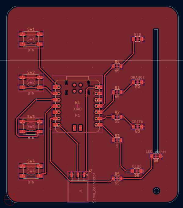
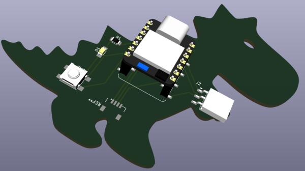
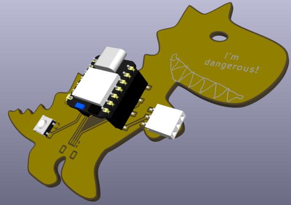
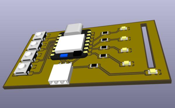
I try to make a simple 3D printed console game out of the simulation above. The story is to remote drive a robot to a charging point, because it has run out of power. In the console there are four buttons, four leds, and behind the leds is a 3D printed robot connected to a servo motor that slowly moves the robot towards the 3D printed charger on the console. It takes 100 correct button pushes, as in the simulation, to finish and if finished, a white led on the robot starts to blink as a sign of charging. Pressing all the buttons at once starts a game. This way I can try out simple input and output mechanisms along with the design and PCB printing.
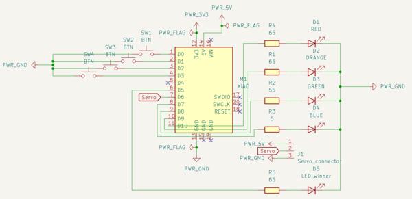
I begin by creating a schematic in KiCad with a XIAO 2040 board (because that I have used previously). First I placed power symbols and flagged them. Then I placed resistors and LEDs to the right side and connected them to the pins that are on the right side of XIAO RP2040, and grounded them. Then I placed buttons to the pins on the left side and grounded them. Finally I used label and a pinsocket to create a connection for servo motor and wired one white LED to be the robot's LED. Then it looked like this.
I checked the fablab inventory and it has 5 ohm, 45 ohm, and 100 ohm resistors to choose from, so I select 45 ohm for red, yellow and green, and 5 for blue. They are lighting up so shortly anyways, so lower resistance is fine.
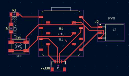
Switching to PCB Editor and updating PCB from Schematic, I continued to construct the layout. I soone realized that the pin0 zero of XIAO and every pin in the schematic editor has one larger number than XIAO. Thus the red LED is connected to the left side of the board. I switch back to the schematic editor to fix this cosmetic issue by switching servo pin and red LED pin.
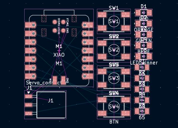
I placed to LED to be at the same line than the buttons, and other parts in their places as I saw fit (without knowing too much about good places), and connected the. I left grounds unconnected waiting for the filled zone.
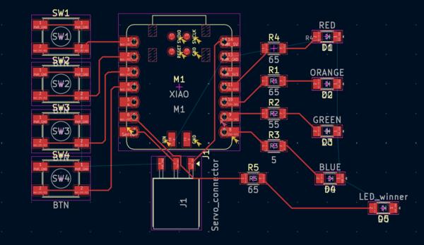
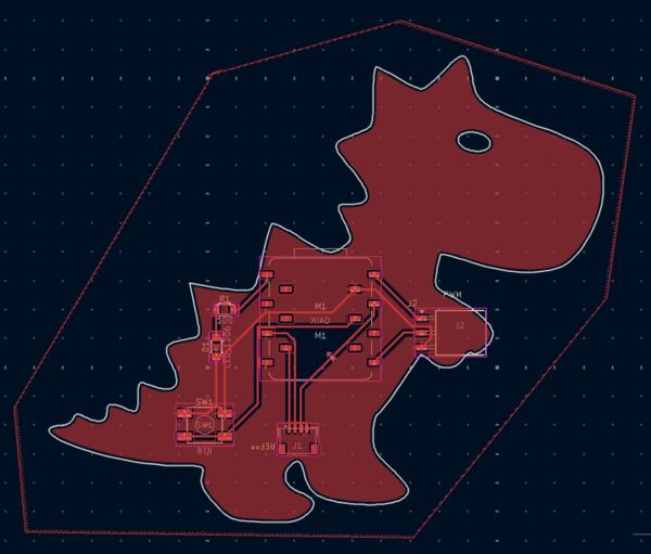
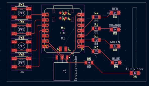
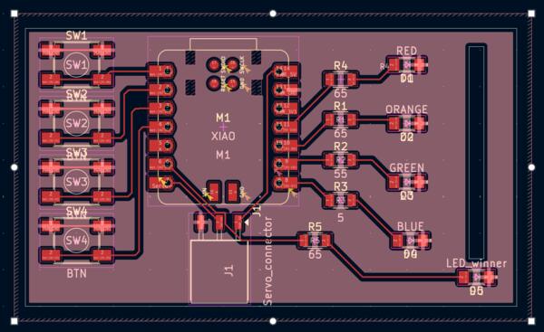
As I was placing the components I got the idea that I dont necessarily need a 3D console, but can integrate a track for the robot on the board itself to simplify test process a bit. I decided to try that out by drawing an outline for the board and with another rectangle creating a track for the robot.
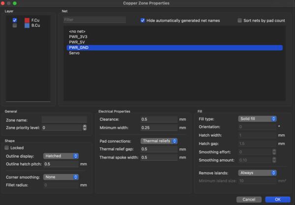
Then I Filled Zones on the front copper (F.Cu) layer and connected it to ground.
Now running a DRC I get a list of errors that I don't understand. I leave this for tomorrow to figure out.
One more thing... I want the corners of the board to be round so I went back and did the Edge.cuts outline again following this tutorial by Kody Rogers. Here it's important to have a pin-symbol showing up when connecting the lines to arcs so that they really become connected. Then did the fill zones etc. again.
And I realized I haven't paid attention to the size of the board so that it can be played. This also likely solves the main errors in DRC, based on what I understood Gemini's explantion of the error and it's fix.
It didn't, but only increased the errors as now also the outlines are "malformed" which seems to be impossible to fix as the outline are as connected as they can be.
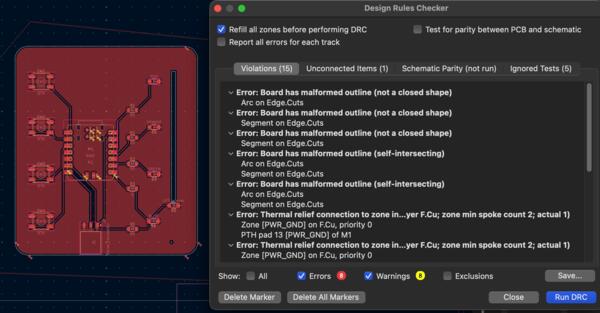
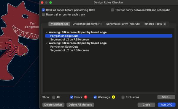
Eventually I discovered that there is a specific "pin" symbol when connecting the outlines that makes them actually connect. Rerouting in more spacious way solved the Thermal relief connection to zone incomplete - error. There was also some automatic texts on the board that were out of bounds so I tried moving them but ended up removing them, I don't know if it's gonna be a problem later.
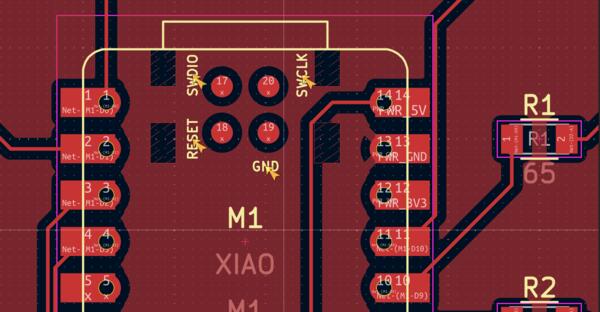
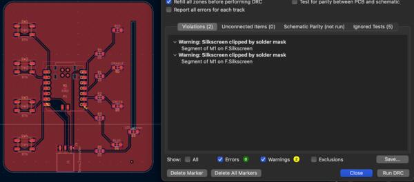
Now I have some silkscreen warnings, but I assume they are not going to be a problem as I'm not using silkscreen with this board.