Week 08: Input Devices
The main outcomes for the week
I experimented with making a touchpad that senses the location of a pen, but couldn't make it work properly.
So I made a simpler sensor device with Time of Flight proximity sensor: when hand is nearer than 10cm, the led starts blinking:
Design files made in these week are available at my gitlab repository
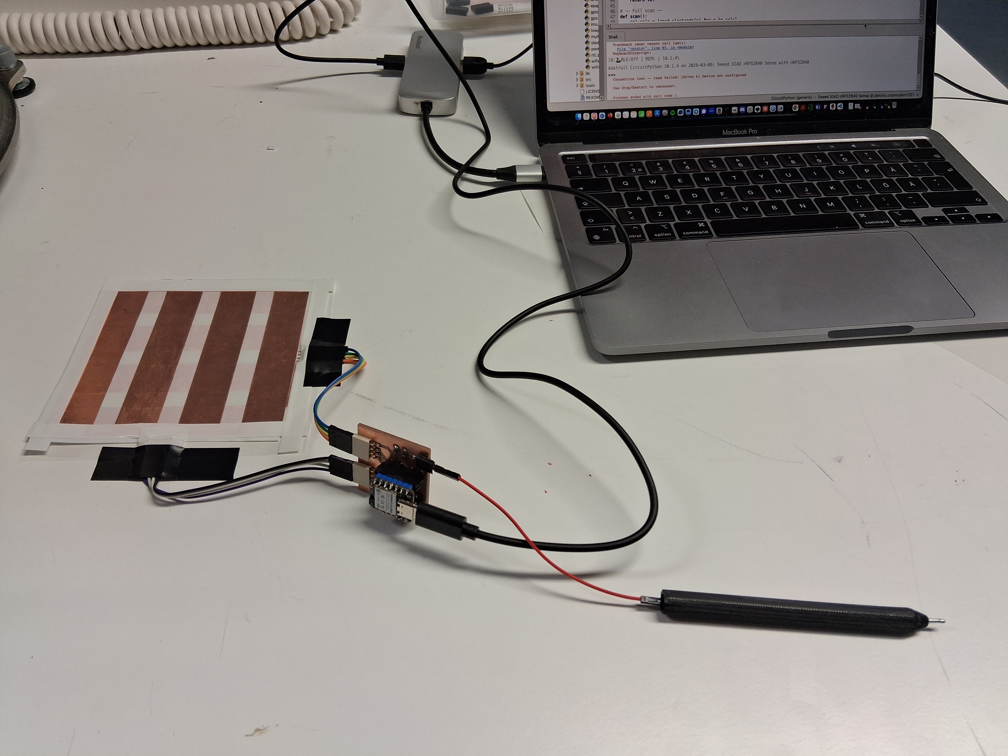
Making a simple stylus pen touchpad
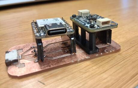
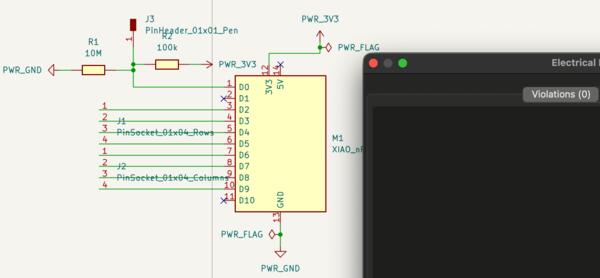
This week (which is going to be submitted late), I'm planning to make a simple prototype for my final project idea of a portable notebook. It has a 4 horizontal and 4 vertical strips of copper tape wired into XIAO nRF52840 Sense board which has bluetooth for future applications. There's a pen connected to pin A0 and there's 100k ohm pull-up resistor and 10M ohm pull down resistor between the pin and pen to make the pen sensitive to voltage changes. The copper strips are given pulses in different times that map the location of the pen. This architecture was designed with Claude given the Rand Tablet as context and it made the following diagram of the solution.
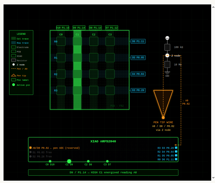
XIAO nRF52840 pin map:
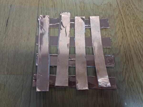
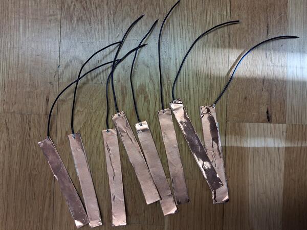
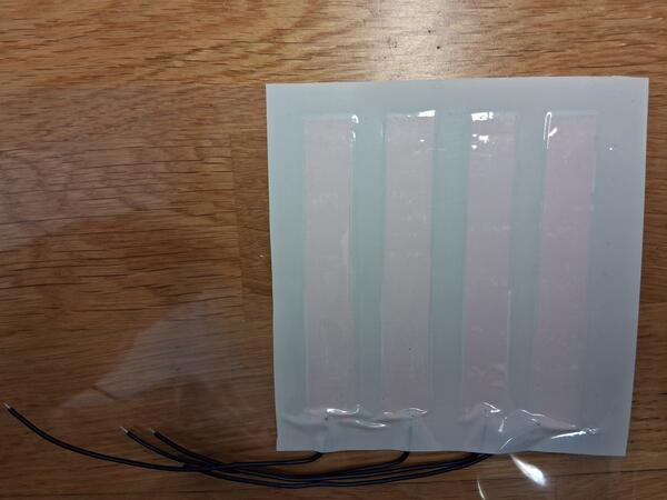
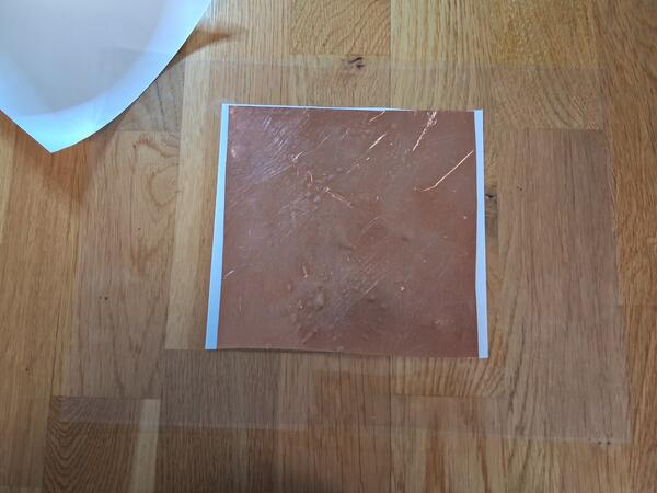
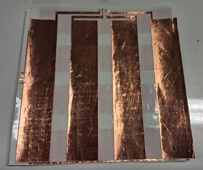
I opened Getting started page for XIAO nRF52840 Sense and collected the copper tape, a transparent film as a surface to place them on on and some glued transparent epoxy plastic for an insulator between and on top of the copper strips. I cut 8 15mm wide 100mm long strips of copper tape and soldered 120mm wires to them before gluing them to plastic surface. The wires should be as short as possible to avoid them sensing "noise" electricity. They should also be the same length to get equal sensor input from each of them.
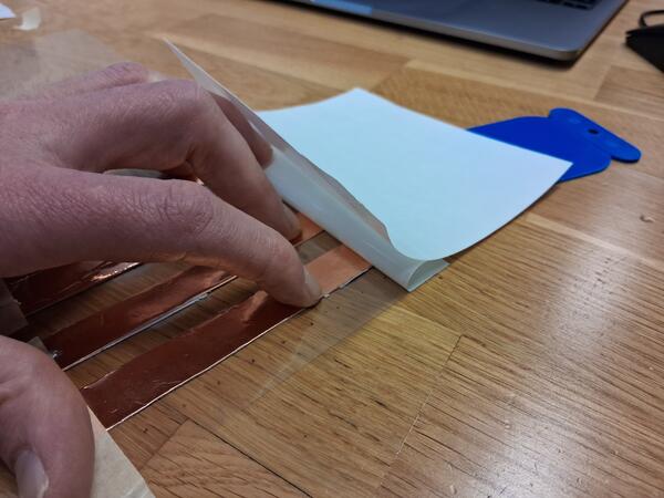
As I had the wires soldered, I placed the stripes on transparent film and began placing epoxy "tape" on top of them. Here I wanted to have all the air out under the epoxy, as it would disturb sensor input making it uneven. This wasn't fully possible but made my best with a flat tool that is used for vinyl cut weeding.
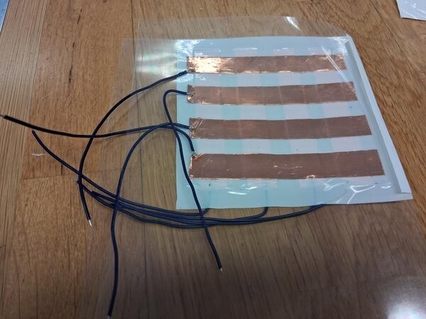
Then I place the second layer of strips. I become more and more convinced that it's impossible the calculate an accurate location based on these rather inconsistent copper strips, but let's see. Now I also remembered that the copper strips are also tape, but I hadn't taped the first layers.
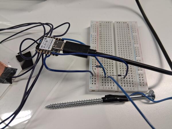
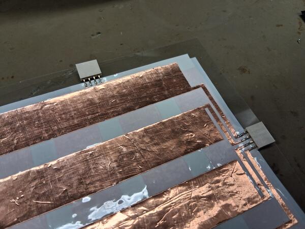
I set the thing up with a bread board to test it quicker than by soldering things (and possibly resolder multiple times). The right resistor is 10M ohm and it's wire is connected to GND and the left is 100k ohm and is connected to 3.3V. In between is the pen wire.
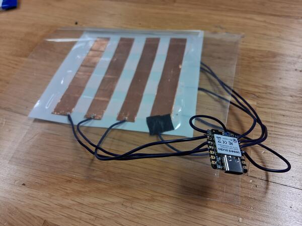
Trying to set up the XIAO nRF52840 for MicroPython with these instructions, because I'm more adept in python than arduino-language. The problem I was struggling with that the firmware available has only flash.bat file which I caanot open with MacOs. So, I wasn't able the have the XIAO connected to Thonny.
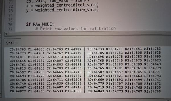
I turned to CircuitPython, which was easy and quick setup: I downloaded CircuitPython .uf2-file from here and moved the file to the microcontroller folder. I had made it visible on my computer by double-clicking the reset button on the board. Then I copy-pasted the code by Claude to code.py file inside the XIAO board. Now I can get some numbers out, but they don't make much sense. Here are the input of values of one circular movement around the area.
Next iteration: PCB milling
Instead of starting to debug this tangle of a device, it can work as a first iteration, and I'll continue to cut an actual PCB for it. I'm gonna make two boards: one is the copper stripes vinyl cut in two layers with 1x4 connector on each and the second is for the XIAO board and two 1x4 connectors.
I begin by opening KiCad and creating the board for XIAO. For that I placed Generic XIAO board and two horizontal 1x4 pinsockets for rows and columns, connected the correct pins on XIAO. Then I also added 1x1 horizontal pinsocket to connect the pen wire and the resistors. And then did an ERC with no violations.
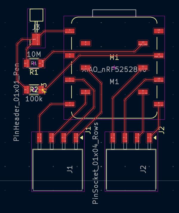
Soon after switching to Layout Editor I had to get back to Schematic to fix the pin connections as they are numbered differently from the actual XIAO: the numbers are just Kicad representations, not the XIAO pin numbers. Below are first the pins connected wrong and then the correct way. This was important for gettin the wiring go smoothly in the layout.
I designed the board to be attached to a corner of a 3D printed case (hypothetical at this point) under the touch pad. The USB and pen would be connected from the outside of the casing and the copperstripes invisibly inside the casing. I also did the Fill zones as ground.
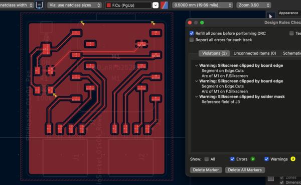
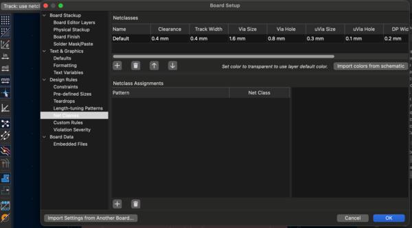
After having the tracks in their place, Kris reminded me about the thing that I had forgotten previously: open net classes, and most importantly, set track width and clearance to 0.4mm (as in image below). Then I had to reroute the tracks to update the width and clearance.
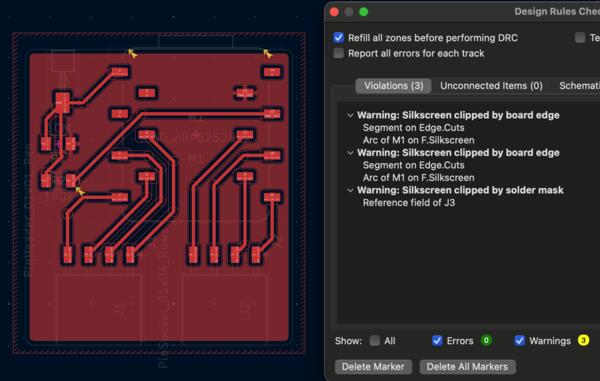
To fix two of the DRC warnings I expanded the top edge of the board, so that connectors were within the boundaries. I also decided to make the board a bit wider to be able to attach it to the case if needed at some point. This change is visible below.
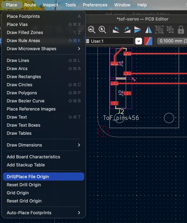
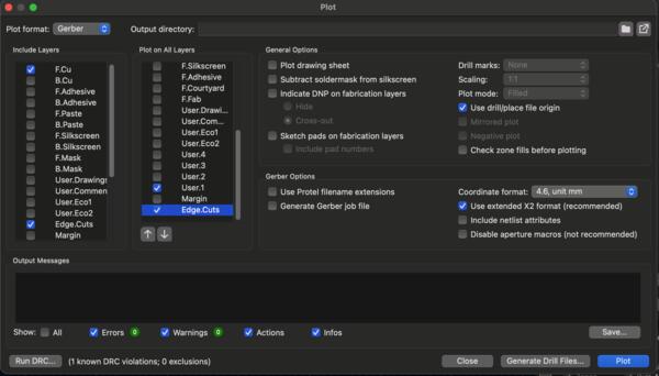
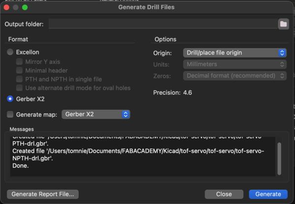
Then, Place > Set Drill/place origin and placed it to the bottom left corner and then exported gerber files at Fabrication Outputs > Gerbers.
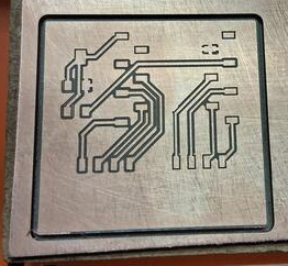
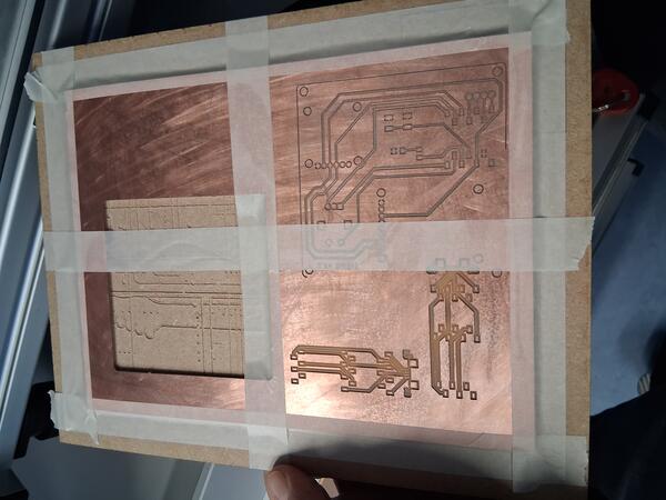
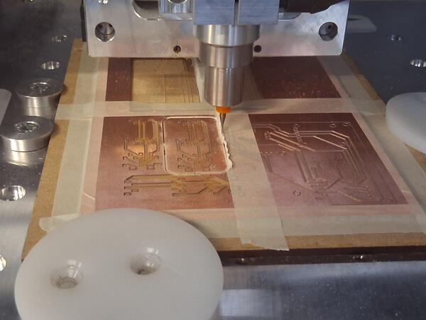
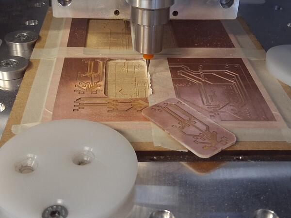
Now in CopperCam, I imported the two layers, did the path contouring and generated the milling files. The outcome was good enough. First time I succeeded to make a PCB with Roland SRM -milling machine. The track are not exactly even but enough.
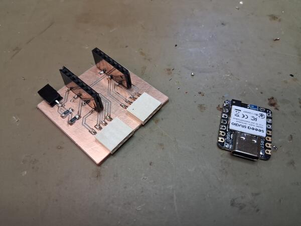
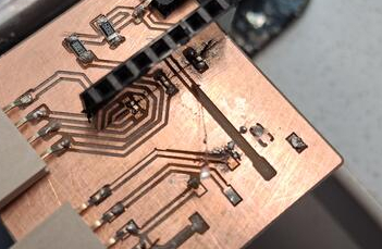
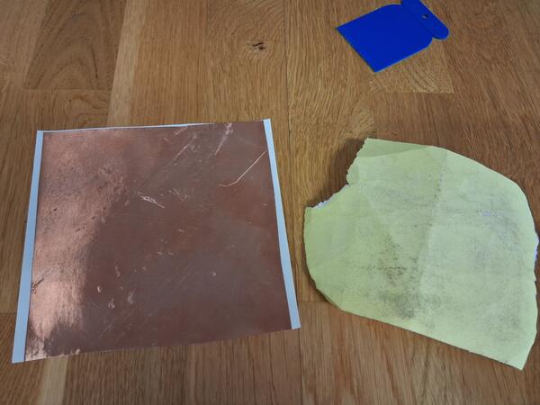
Then I began soldering the components on the board. I used connectors for the XIAO board as in the board on the left in the first image.
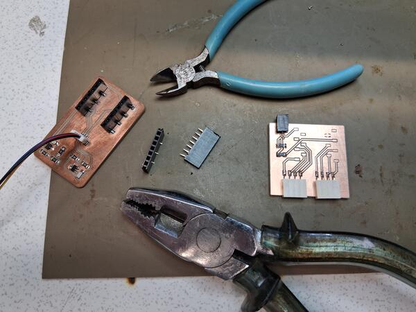
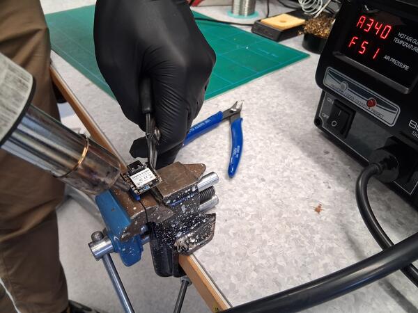
Everything went surprisingly smoothly, until I had only the XIAO board to solder. The difficult and frustrating part was to remove all the solder from the board I had used before. It took about an hour or more to have the pins clear enough to have the "legs" go through them. After complaining to Kris about it, I came to learn about a hot air gun which the more optimal solution for this. I also learner that using flux pen before trying remove solder with rosin braid is agood idea.
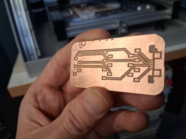
In the end, I managed to finish the board.
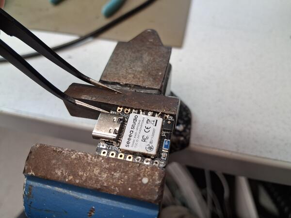
In the end the XIAO board looked possibly damaged so next I connected it to the old touch pad and tested if all the pins are working. So I connected the wires to pinsockets and XIAO board to computer and ran the program. Nothing. There was no lights on the XIAO. But connecting XIAO alone without the board turned the LEDs on so the problem was in the PCB. Looking closely, there was a tiny amount of solder near one pin which had probably caused a short circuit. Using multimeter, I checked al the other connections as well and in the end there was one pin that didn't conduct at all and I didn't know what was the issue, so I changed the connector altogether. While doing that, I managed to ruin the board by ripping off the one track.
Starting from the beginning I had much more trouble with getting the track cuts even across the board. After a few tries, I found this one to be good enough, even though one track, the second from left at the bottom, was really thin.
Then I did the soldering now with a thinner solder and added much less of it. It was quite fast and easy, so I guess I've reached the second level in my soldering skills now. And also all the connections were working when tested and XIAO lightened up as well.
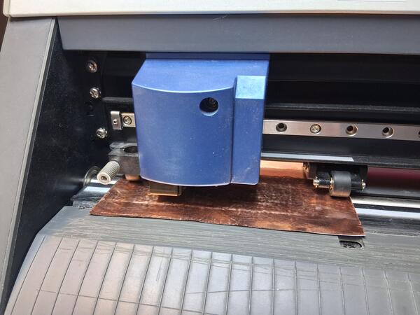
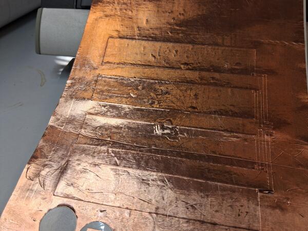
Vinyl cutting copper tape
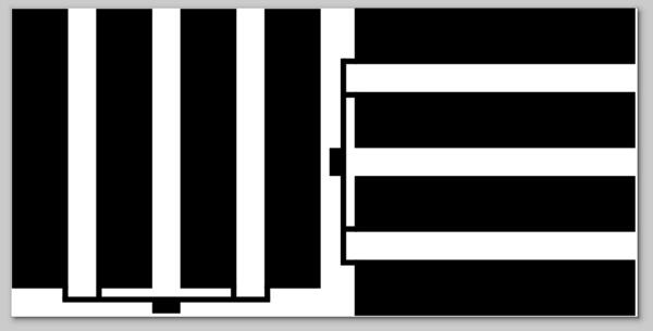
Then I continued to (vinyl) cut the copper strips. I started with making a vector image of them with InkScape. Below is the outcome (which I later realized to be obviously flawed because all the stripes are connected).
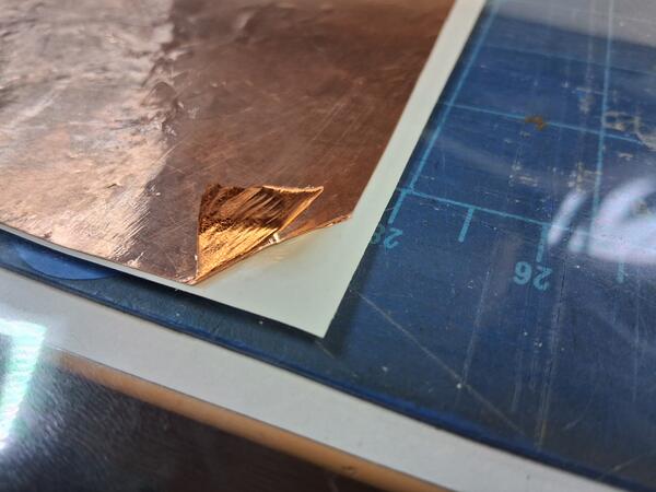
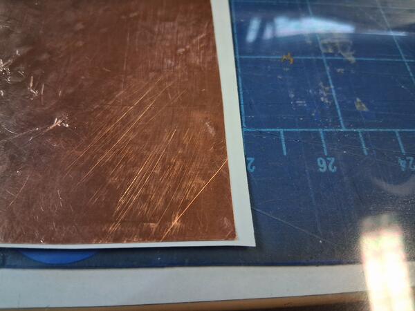
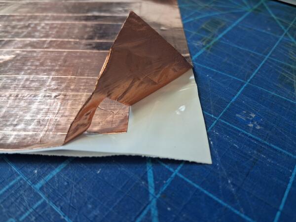
The actual cut material was set up with a piece of epoxy tape, on which was taped the copper tape, and they were then taped on top of the transparent film. We also tested if copper tape has protective layer similar to FR2 by soldering first without sandapapering and then after sandapapering, and it seemed to be easier after scratching the copper slightly.
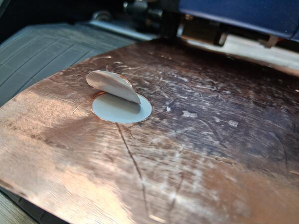
I took the knife out of the cutting machine to check it and set a good depth for the cut. I manually made a cut on the material with the knife. First one was not enough so I turned the knife slightly more outwards and then it was enough to cut the copper layer without cutting the epoxy beneath.
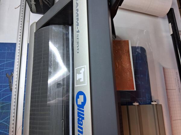
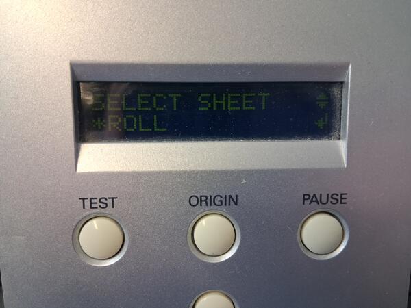
Then I placed the material int he cutter and clamped it on it's place
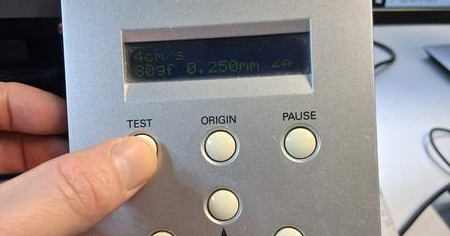
I pressed Menu and Enter to define the material as Piece (it now appears that the the cutter screen is not very visible in the camera)
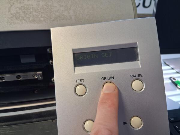
Then I moved the knife with arrow buttons to the bottom left corner of the copper area and long pressed Origin to set the origin and then pressed Test to run test.
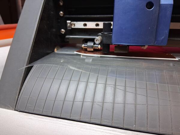
There appeared a problem with the softness of the transparent film so the test failed. The second test was even worse as seen in the video below.
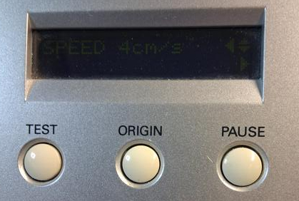
I decided to cut away one side of the transparent film the prevent that from happenging and also halved the speed in the options.
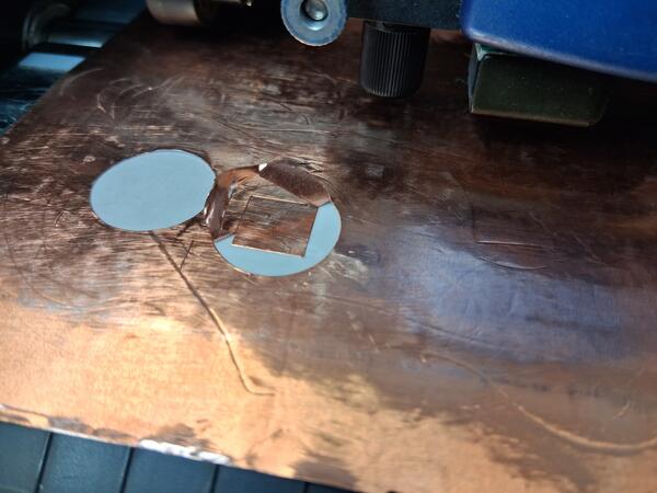
Now the test was a success. On the right you can see the previous try.
As I continued to cut the stripes, a similar problem came apparent. No matter which way I put the material and cut away the transparent film, this kept happening:
The problem is likely the transparent film beneath as it is quite slippery.
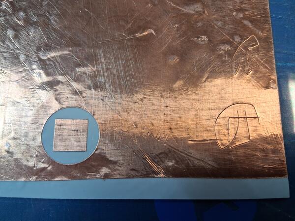
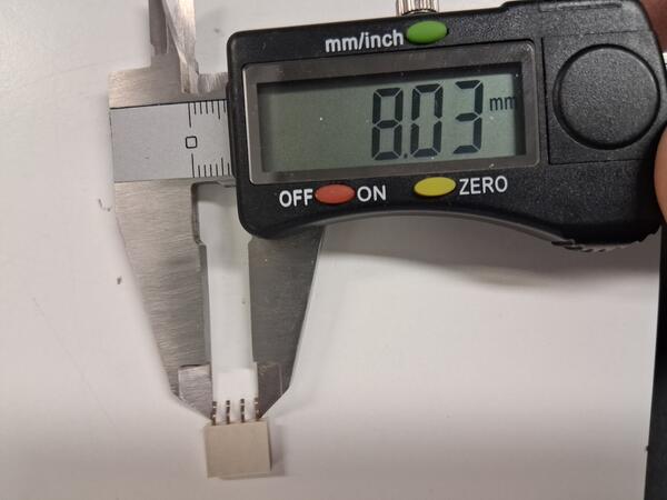
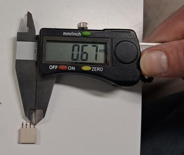
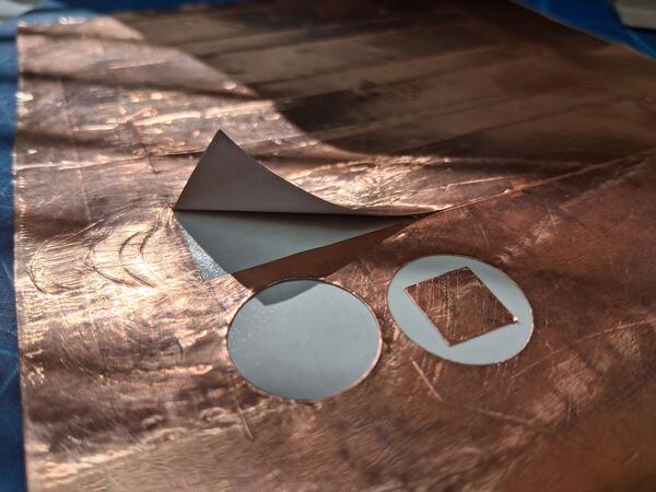
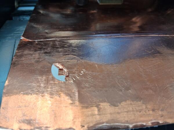
Soon I realized a serious issue with the board design: the copper stripes are all connected to a one and same connector footprint. So to fix the vector image for the next cut, I measured the actual connector that I'll use with the copper stripes and made changes accordingly. I kept as many areas as possible wider to help the weeding after cutting.

Back at the vinyl cutter, I set the roll of epoxy tape to the cutter.
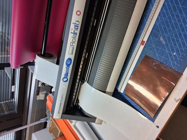
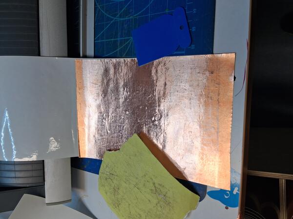
Sandpapered and taped copper tape on top of it.
Cutting material didn’t have to be exactly to the left side but instead needed to cover the optical sensor to be working. The origin is not possible to be set to the corner: should have taped the copper more up from the bottom edge of epoxy tape to save more of it.
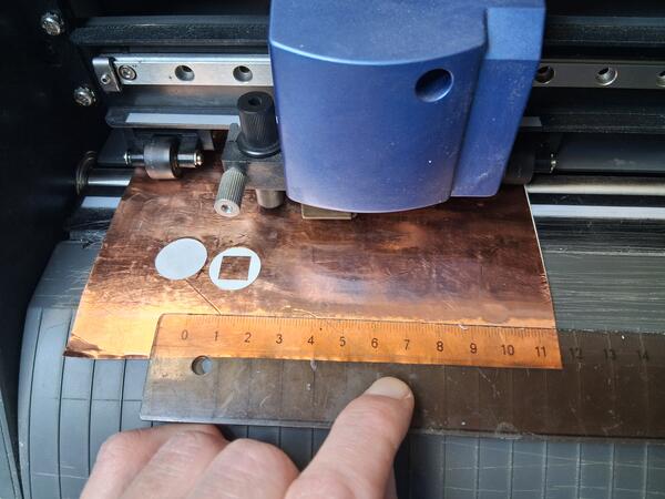
I set the origin as bottom left as possible. Launched the test. I was thinking not to because the amount of copper tape was measured for the stripes, and not the test. Luckily I did because the test cut was too deep: the epoxy tape was also cut. I twisted the knife deeper to its holder and ran another test, which was successful.
The copper stripes are 11cm wide so the whole width where the tests are go to waste…
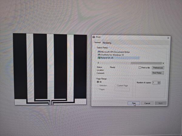
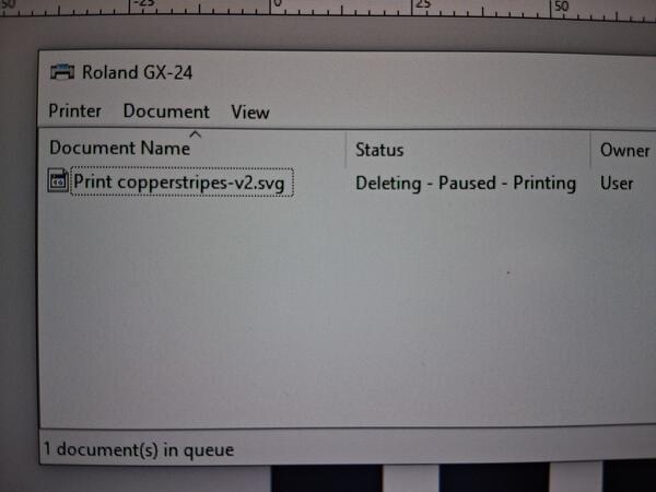
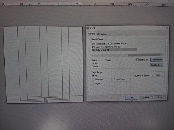
Set the origin to new place and selected print on Inkscape but nothing happened with the cutter. I opened the printer menu and found one project waiting to be printed. I removed that and restarted my print. Nothing. I tried deleting the print but it did nothing. Instead windows told that the status was Deleting - Paused - Printing. I tried restarting the computer. The cut didn’t begin still. I tried reloading the roll. And suddenly it began cutting.
It seemed that there was something wrong as it was cutting only the stripes but not the connections. then it cut the connections last as their own rectangles. I must have forgotten a step in Inkscape to make the lines integrated or something.
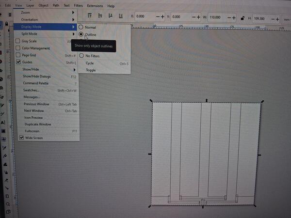
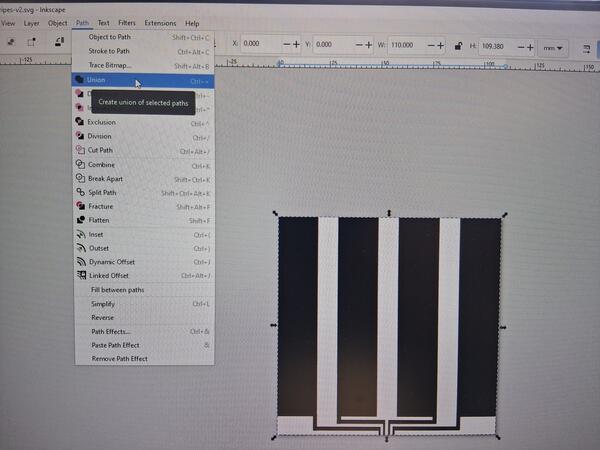
In Inkscape, I first needed to ungroup the rectangles. Then I selected all of them and then Path > Union. It was also useful to select View > Display > Outline. I also added a line on tope of the stripes to have them cut apart from the overall tape.
I also realized that the cut was too deep and the epoxy was cut away as well (the white under the copper).
So I twisted the knife even more inside the holder: now you can barely see it. Now with new copper tape, I have some extra area for running the test.
Loaded the machine again, set origin to bottom left corner, and long pressed Test button. The cut was really shallow but with a bit effort I was able to weed out the extra copper.
I printed the unioned stripes on Inkscape. Again, nothing happened. Tried unloading and loading a couple of times and got it cutting. The result looks a success. I print the second one right after, but quickly pause and cancel the cut because I hadn’t set a new origin and it began cutting the same spot. Fixed that quickly.
10x faster video of the first cutting round (out of two)
The outcomes looks successful. After weeding the first one it still looks goods. On the second cut there’s part where the knife has cut also the epoxy.
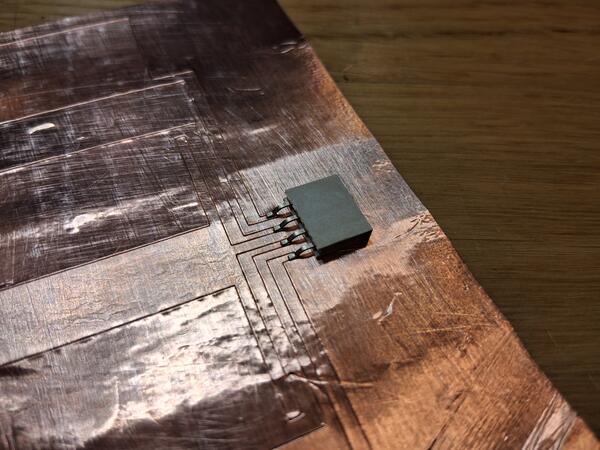
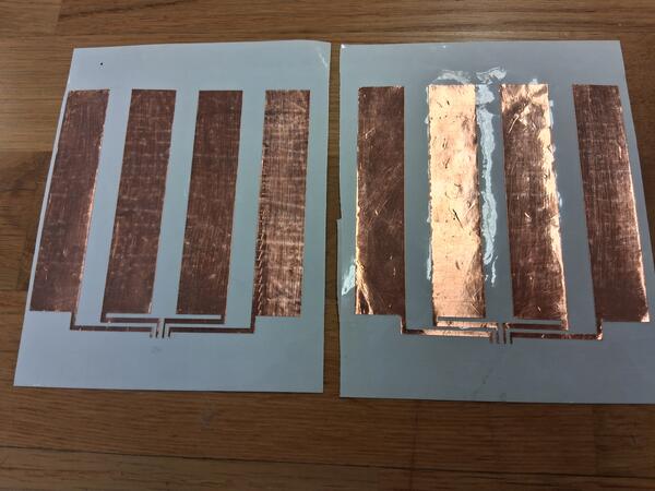

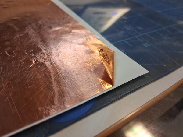
Then I taped the on top of each other and sodlered the connectors. I should have left more epoxy to the sides to ensure insulation between the layers. Now I wasn't sure if that caused problems.
The Pen
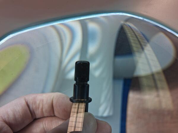
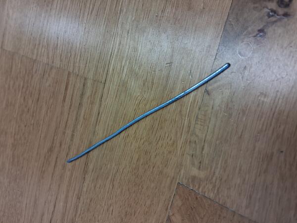
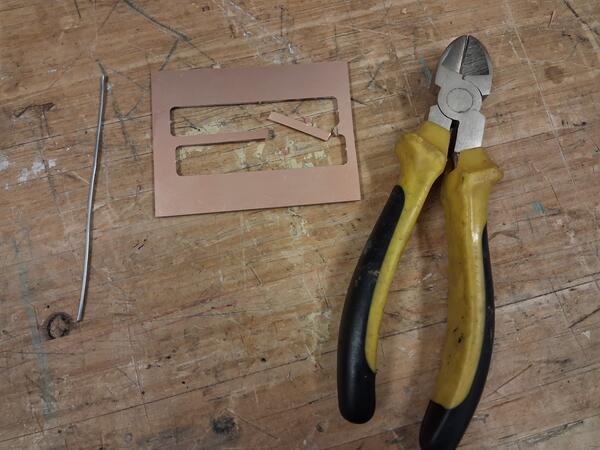
For the pen, I clipped a piece of steel wire and straightened it.
Then I modeled a simple pen with FreeCad where there's a mounting place for a small PCB for a connector.
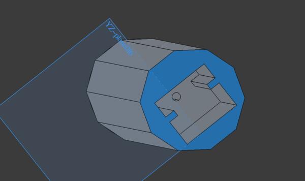
There's also a cone as a tip which I did without sketching on Part workbench. Then I used 1.6mm cylinder to cut a hole through the cone/tip and the pen for the steel wire.
The first print had again too small parameters: the hole obviosly wasn't going to stay at 1.6mm.
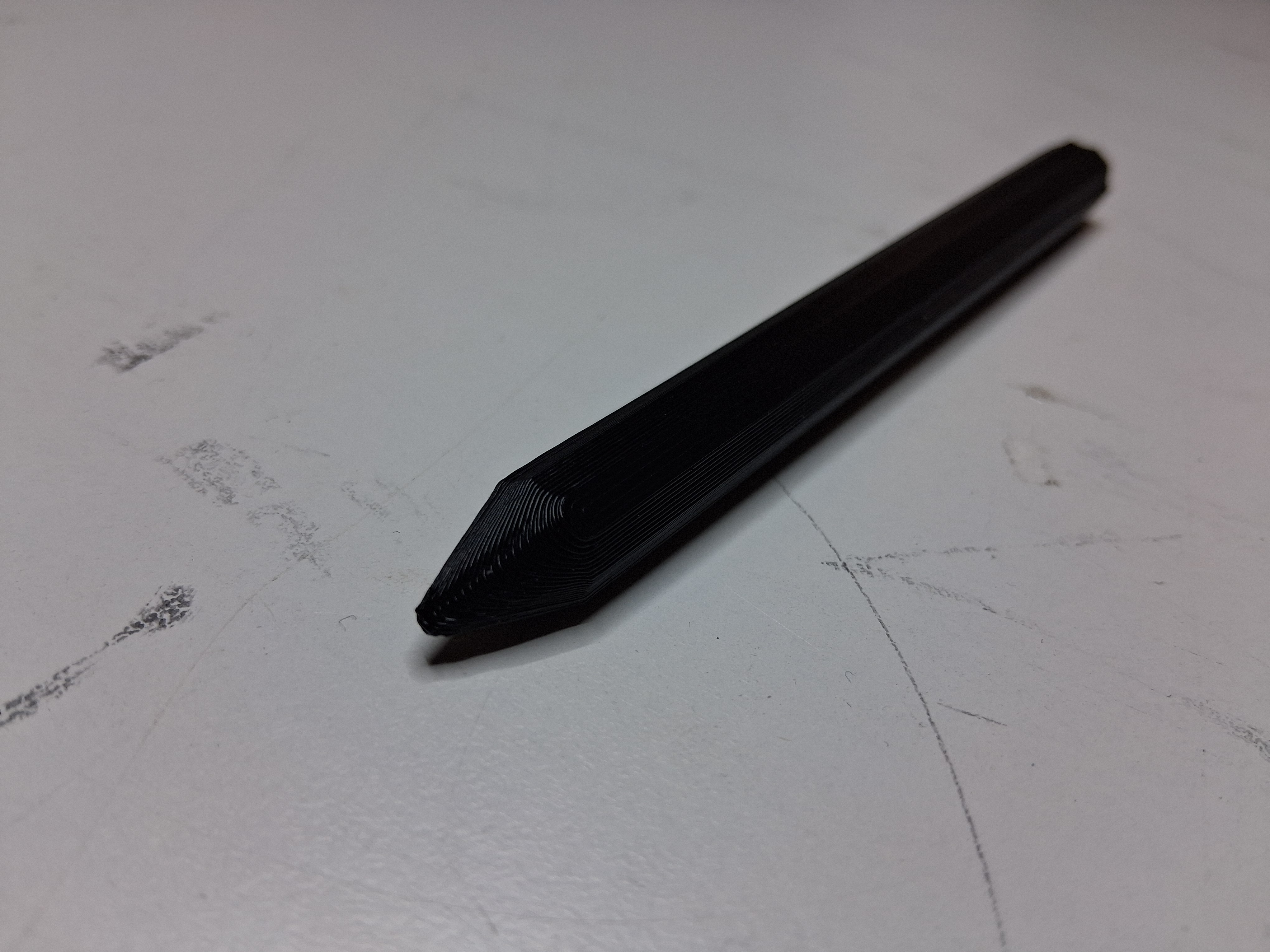
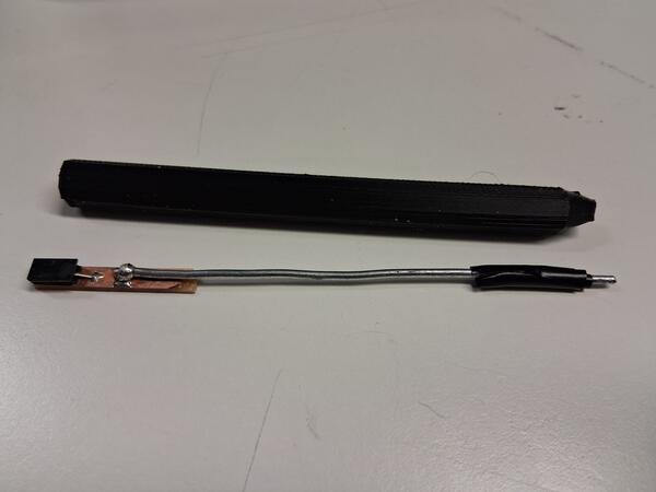
I made a new pen pin 6mm hole. I clipped a piece of FR2 and soldered metal wire and connector to it.
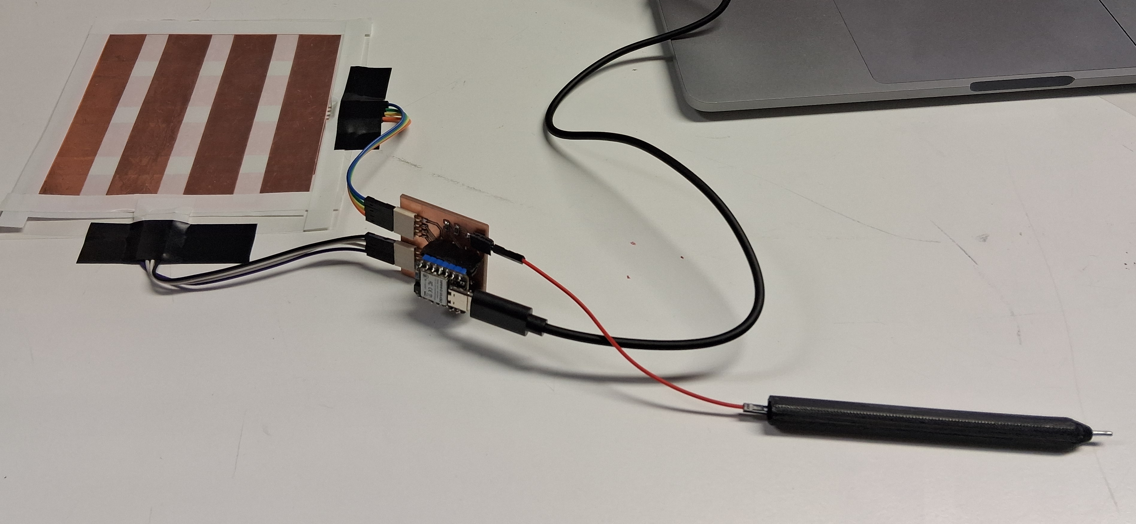
Testing
Then I plugged the wires in and tested the code on the computer.
It didn't: the location showed that the pen is in the middle while I was circulating it around.
Analysing the values in RAW_MODE in which the signal strengths had been scaled in between 0 and 65535, I had only values on the upper end. This means that the pen is saturated, and cannot receive any stronger signal than what it’s receiving from electricity from the environment. Thus the program calculates the location in the middle of the pad as all the stripes are giving full signal from the pen’s perspective.
I tried to debug with Gemini this issue. Plugging the pen out and not seeing any difference in values tells that the problem is in the board, not pen. Connecting the pen wire directly to ground tells that wiring is working but the idle state is too high.
Used multimeter to spot whether the connections work and everything was fine, except the 10M resistor values were varying a lot: it showed around 15-25M ohm resistance, and 350k if measured in other direction. I tried with another multimeter and got the same results.
I tried changing the 10M resistor. After desoldered and removed from the board it showed exactly 10M ohm resistance. I put another 10M ohm resistor and after being soldered it shows something like 2M ohm resistance and then the value moves up slowly. There seems to be something wrong with board on that spot.
I swapped the places of the resistor and got the “noise” output to under 1000. Some of the columns give some reasonable output but the columns (under the epoxy) barely any.
Suggested by Gemini, I increased THRESHOLD, and ended up calibrating to 4000 and SAMPLES = 20 to decrease variation. Still not much progress: I get mostly 0,3, as locations.
I should somehow be able to widen the gap between noise and signal. The problem can also be that I cut the epoxy tape too close to the stripes and they are leaking around the edge to each other. Overall, there are too many issues with this project so I moved on to make a simpler input device.
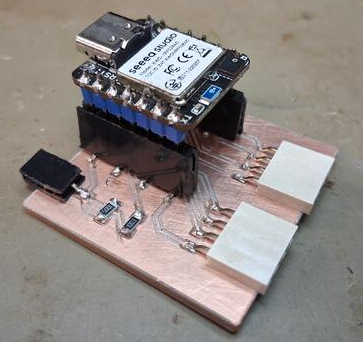
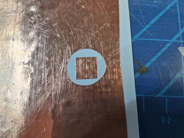
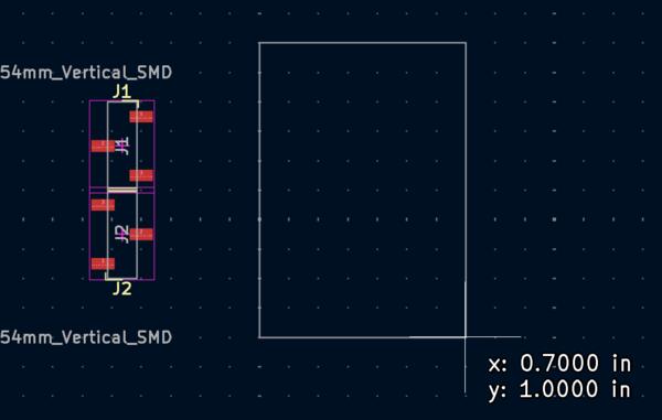
ToF proximity sensor board
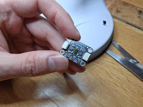
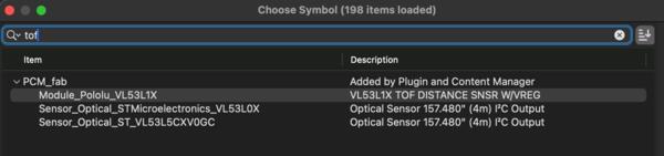
Began by creating a new KiCad project and modeling the first board with Schematic editor. There is no ready component in the Fab library so I will just use two horizontal pin sockets on the board to match the pins on ToF.
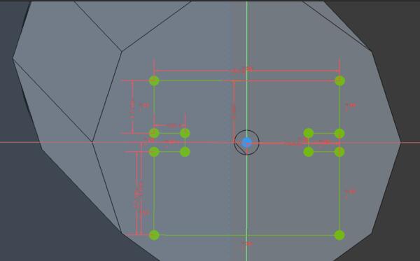
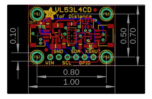
Updating the two sockets to Layout editor, I will lay the outline for the ToF-chip. The dimensions and pinout are are shown below and were accessed here.

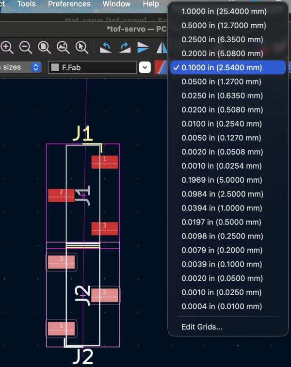
I set the kicad grid measures to 0.1 inch so that I can place the sockets to 0.1inch apart as shown in the dimension image.
Then I used the rectangle tool to outline the chip. I got the dimensions visible by clicking and lifting the click before drawing. To be able to place the sockets on the chip outline, I needed to set the grid to half, to 0.05inch
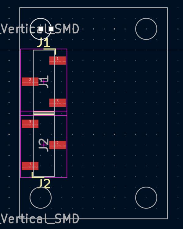
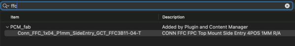
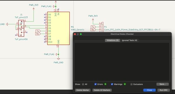
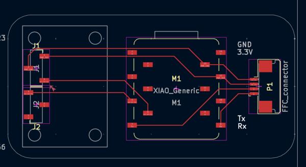
Then I went back to Schematic editor to draw the wirings and also adding XIAO board and FFC (flexible flat cable) connector
Using the Schematic view, the wires are: pin1=3.3V, pin2=GND, pin3=SCL, pin4=SDA, and pins 5 and 6 go nowhere. In XIAO SDA is D4 and SCL is D5. Tx is D6 and Rx is D7 which connect to the FFC (flexible flat cable) connector.
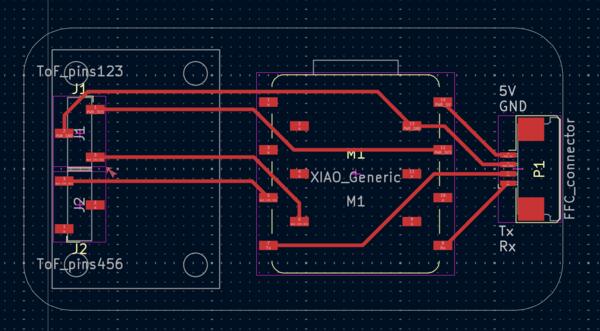
I change the routes to FFC to match better their location on XIAO board: left one is old and right one the new order.
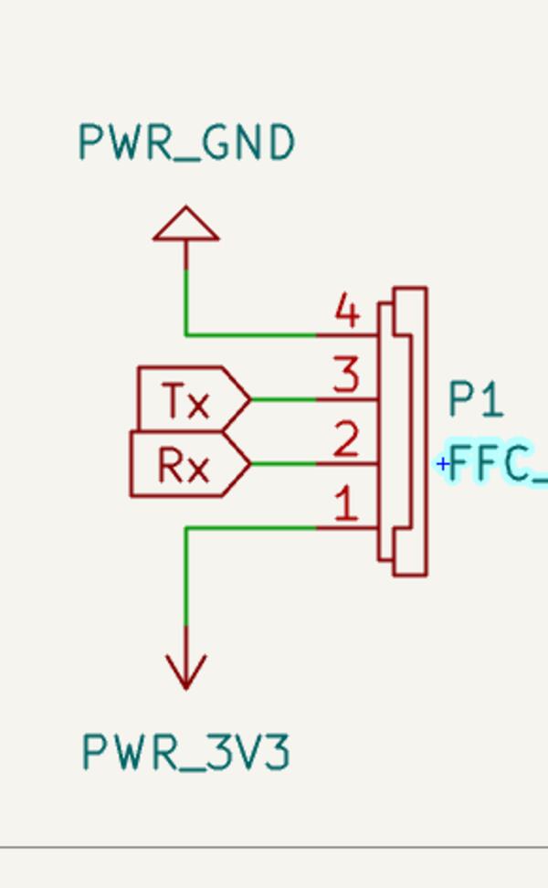

I also added text to the board on user.1-layer to show which connections are which on FFC.
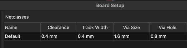
Now before going forward to exporting gerbers, I remember to set the track width and clearance to 0.4mm on Net Classes setup. This should be done before setting the routes because it doesn’t update them automatically. On the bottom right corner I selected only Tracks, CMD + A selected all of them, and pressing E opens edit menu where I set the track width to 0.4mm.
Then I also added the Drill/Place File Origin to ease up the alignment of all the layers on milling software.
I did the usual exportation to gerbers.
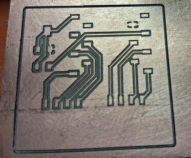
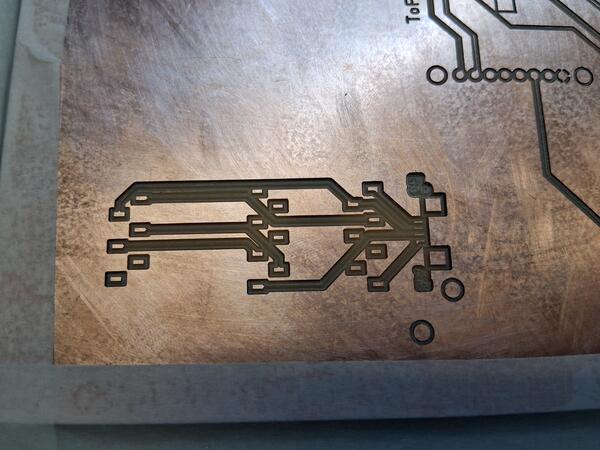
I moved the gerbers to the computer at the Bungard milling machine and opened them one by one on CopperCAM. I added design tabs and calculated the contours. Also checked that the tools were as supposed to be. The pressed Mill and saved the plt-files, which I opened on RoutePro3000 and followed the same instructions provided at aalto wiki as before.
It appeared the PCB was being milled in different axises that I thought, even though particularly consider the different axises on Bungard. However, the board seems to fit next to someone else's failed board.
The engraving turned out to be too deep. I tried changing the thickness parameters slightly.
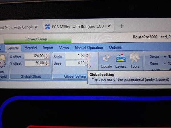
It is still too deep.
This is actually because the PCB material is not attached properly and is “jumping” as the mill moves up and down.
I detached the tapes and placed some new ones.
Now the jumping stopped and the engraving worked.
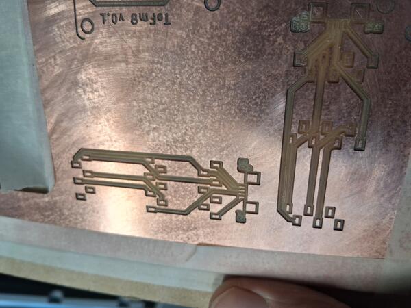
The text should be larger, though. (Later note: the text layer should be added as an extra engraving layer on copper cam after clicking Mill.) Then I changed the bit to the drill and selected th T4.plt-file to cut the outlines. It appeared that the space was too small and it drilled over the taped. I hope that is not gonna do any damage on the bit.
Suddenly the PCB detached too early so I stopped the milling. Everything was fine though with the board (only afterwards thought that I should have also checked the drill bit).
Being already in a bit hurry, I quickly soldered the components on their places.
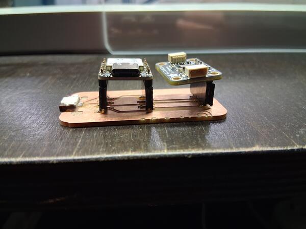
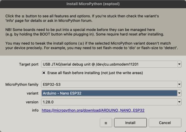
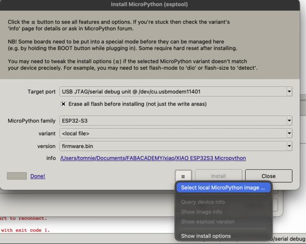
I connected the XIAO ESP32-S3 to my computer and began installing micropython on it. I first tried Tools > Options > Interpreter and chose the USB port and clicked Install or Update MicroPython. Although everything seemed to go well, I couldn’t get the board connected.
I went to Seeeds Studios' ESP32-S3 MicroPythin tutorial page but it was on windows so it wasn’t for much help, only that I downloaded the firmware. I asked Gemini for help and ended up installing micropython with the downloaded firmware (by clicking the three lines button and browsing the downloaded firmware file on my computer).
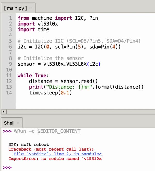
Now I got it connected and the LED blinking. Gemini gave me this code for the proximity sensor but it gave the error:
I installed the driver for VL53L4CD with this terminal command:

which was provided at Adafruit's ToF tutorial materials
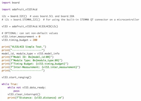
From that same resource I copy-pasted the basic code for the sensor board. Both of these (this and the dimensions map) VL53L4CD resources were found behind ToF's product page's Learn section.

Now the code gave me error: no module named 'board’. Asking from Gemini, I realized that this code was for CircuitPython, not Micropython. It also gave me the code for MicroPython which I then copy-pasted in Thonny. I tried it but realized soon that also the VL53L4CD Library was on CircuitPython, wonder if that matters, and yes that was actually mentioned by Gemini as well, but had given me non usable solution for it.
Anyway, I ended up installing CircuitPython and got the following help from Gemini.
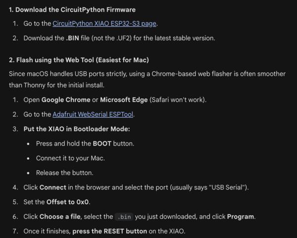

Links from above Gemini-image:
Firmware:

Web based flashing:
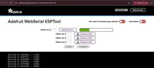
CircuitPython Adafruit library bundle (I did this anyway, although I had already installed the library with pip, because I wasn’t sure if where it got installed before.)

After this process, I was able to make the code from Adafruit work.
Documentation for the vl53l4cd library
I wanted to make the integrated LED blink when proximity is under 10cm.
I checked CircuitPython documentation to see how the Pins are addressed.
...

One issue is that the sensor shows 0cm when nothing is in proximity.
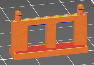
I made a model for a support pad for the other side of ToF on FreeCAD using sketches, pads, positioning (on body’s data tabs) and boolean unions on Part workbench. The first quick outcome looked like this:
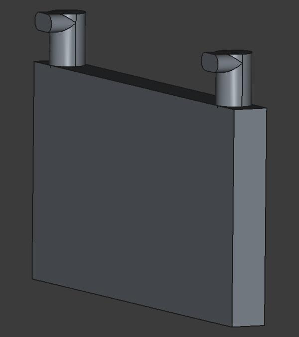
The next day I developed it slightly and printed it like this: