Week 07: Electronics Production
The main outcome for the week
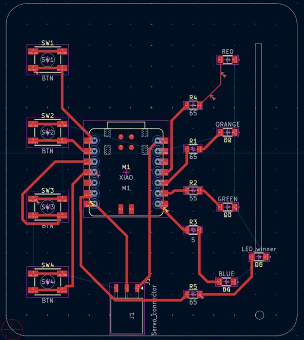
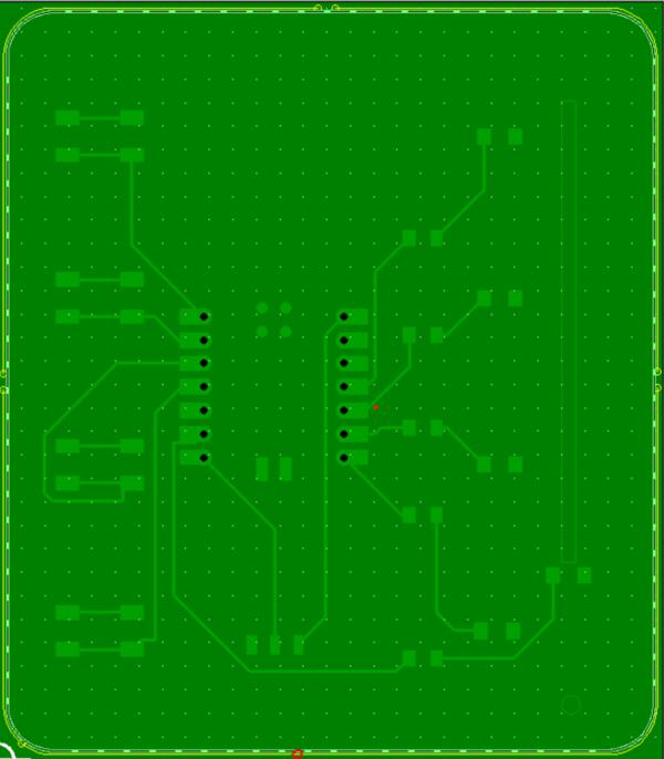
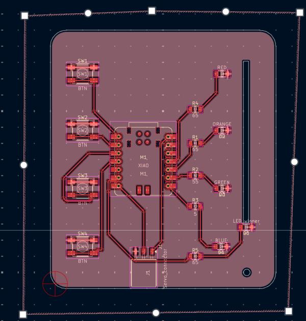
This week I printed and soldered the LED blinking button push reaction game (designed last week):
Design files made in these week are available at my gitlab repository
Hopping one week ahead
Due to the arrangements in our local class, I will do this week as if it was the 8th week in FabAcademy, and return to CNC milling in a week or two.
PCB production process
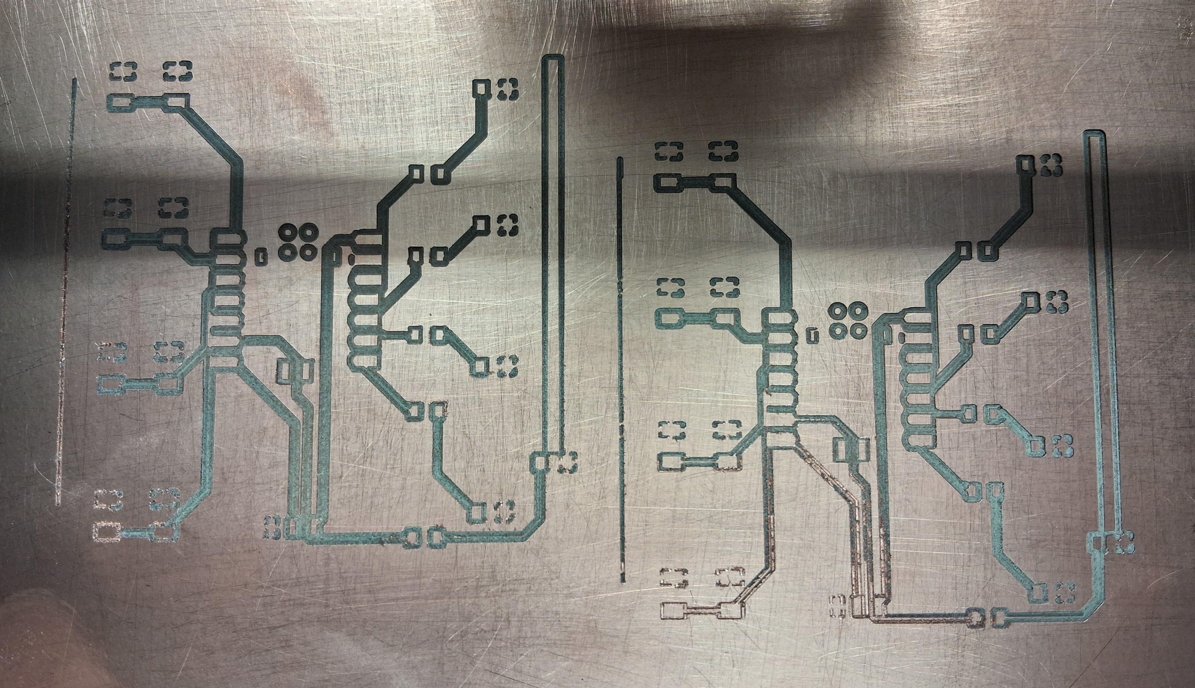
I downloaded this linetest for traces (image below), opened it with Inkscape, scaled the traces to match millimeters (with a 0.5mm wide yellow rectangle on top of the 0.02inch trace), exported it as an SVG, and opened it in KiCad with Import -> Graphics. For some reason the import didn't include the numbers, so I added them to User.1 layer. That probably won't work as also the front copper layer is going to be removed under them. So I returned to Inkscape to do some adjustments and spent too much time trying to figure out why the numbers disappear. So I let it be.
For creating tool path from Kicad to CopperCAM I rely on this tutorial at Aalto wiki. First I ran DRC to make sure there are no violations. Then created the gerber file.
Roland SRM-20
For the use of this machine, I relied also on another the documentation at wiki.aalto.fi. We have two types of tools for milling on this machine:
- Tool 1 is 60 degree ~0.4mm V-shaped bit and it's used for engraving (red collar)
- Tool 2 is 0.8mm router for cutting and drilling (orange collar)
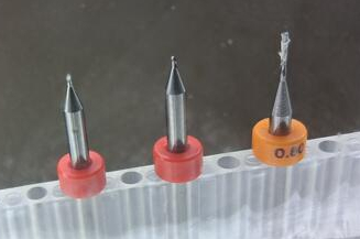
Tool 1 is used first for engraving the routes because it's easier to keep the board in place when not yet cut smaller.
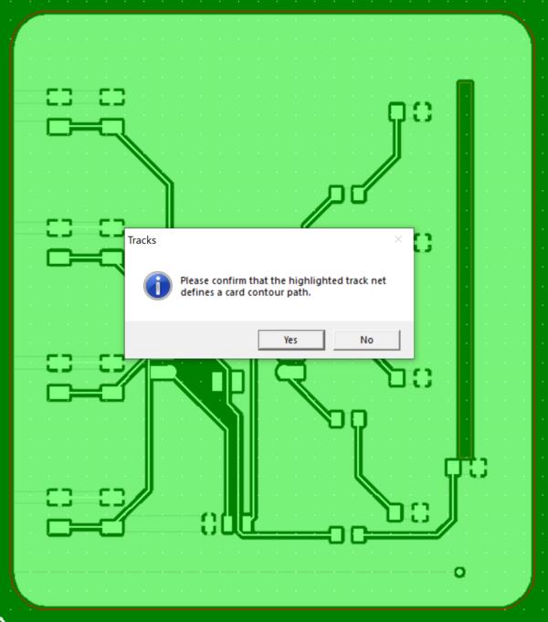
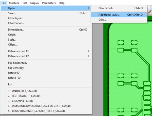
I started with milling my own PCB design for the reaction game. So I opened CopperCam on the FabLab computer and began preparing the files for milling. I opened the boards F.Cu gerber-file (File -> Open -> New circuit) and clicked yes to If the highlighted line is the contour. I did the same again for the Edge.Cuts-layer with File -> Open.. -> Additional layer and clicked yes for contour.
The layers weren't aligned so I followed the instructions to align them. It didn't work because for some reason I couldn't select the edge.cuts layer. I also realized I hadn't placed the via in bottom right corner in Edge.cuts-layer so I returned to do it on KiCad (on another computer) and exported the gerbers again (via OneDrive). It didn't go as planned either, because the via wasn't visible even if I did it on edge.cuts-layer. I tried to make a simple circle instead, but for some reason KiCad only drew rectangles even though the draw circles was selected. I quit KiCad to reopen it and it wasn't to be found in the applications. I searched for it and eventually found it and it still didn't draw circles.
At this point I had already used 1.5h trying to figure some basic things out and I hadn't even got started with the milling.
Well instead of circles, I made two half circle arcs and connected them and this way I got the hole visible in gerber view. The hole is for possibly attaching the servo motor to the board as for the possiblity of using the board as a console (I'm not sure if it's going to work). Then I uploaded the new files again to OneDrive to move them to the milling computer, and now OneDrive gives and "Unknown Render Failure" out of the blue. This seems to be my workflow all the time: struggling with random obstacles that are not about the actual work that I'm trying to do. So I emailed the files to myself and opened them in CopperCam and now the edge.cuts-layer comes up only as a dim rectangle in bottom corner.
I tried sending it again and suddenly it appear as it's supposed to. But I still can't align it with the front layer because I can't select the edge.cuts area at all, it won't respond to any clicks. Maybe I have done something wrong / not done something right in exporting from KiCad.
I turned to Gemini to ask how to align the layers. (Later note: Right click and Set as reference point and so on) It can't seem to help with the issue I'm having on CopperCam but recommends aligning them already in KiCad so I try that. I try sending all the my KiCad files to the lab's drilling computer and open them on KiCad. It appears that KiCad is not configured on the drill computer, so I end up doing it on my computer anyways.
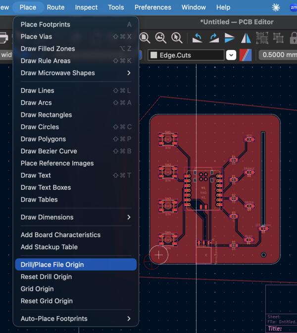
Around a few more corners, I select Place -> Drill/Place File Origin and set the origin in the bottom left corner of the board. Exporting to gerbers, I selected Use drill/place file origin. Also Gemini instructed me to generate Drill files (which I hadn't done previously) and select Origin: Drill/Place file origin.
Again I emailed these to the lab's drilling computer, opened them on CopperCam, and now I had them already aligned. Finally the first step in the process and it's already almost lunch time. But I managed to manage my frustration.
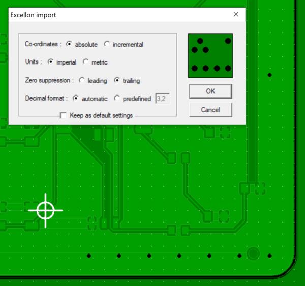
Now trying to open the drill files, CopperCam places holes in somewhat random place. Apparently I need the holes for the XIAO board to be attached to the board. After a few tries, I realized that by toggling the Units to Imperial then the holes where in their right place. The NPTH.drl-file is not opening at all, but it seems I don't need it.
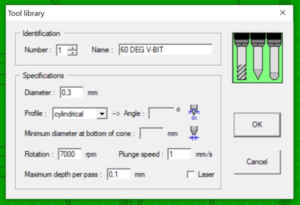
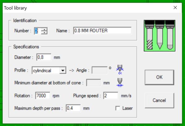
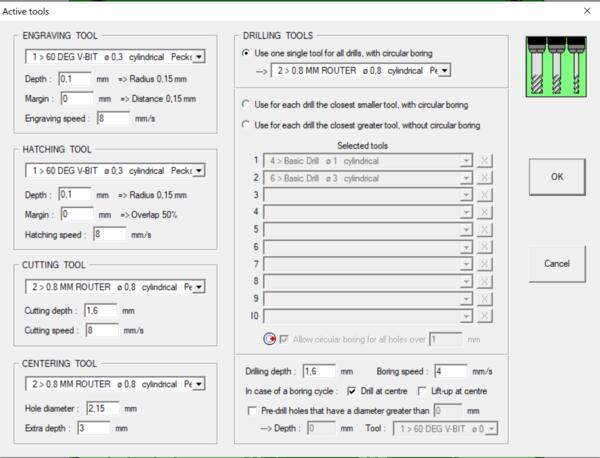
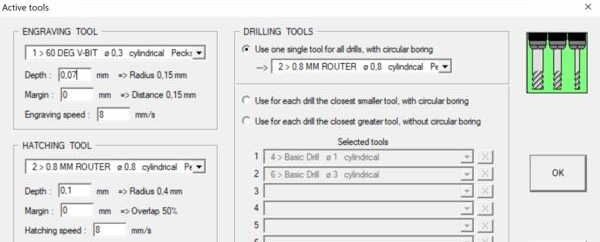
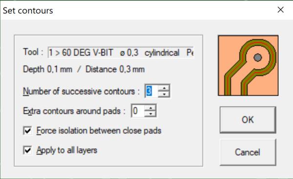
I calibered the board to be 1.56mm so I set the dimension to 1.6mm and margin to 1mm. I also checked that the tools in CopperCam are the same that are in use (match the image at aalto wiki). At Parameters -> Selected Tools, I check that the Active tools match the instructions.
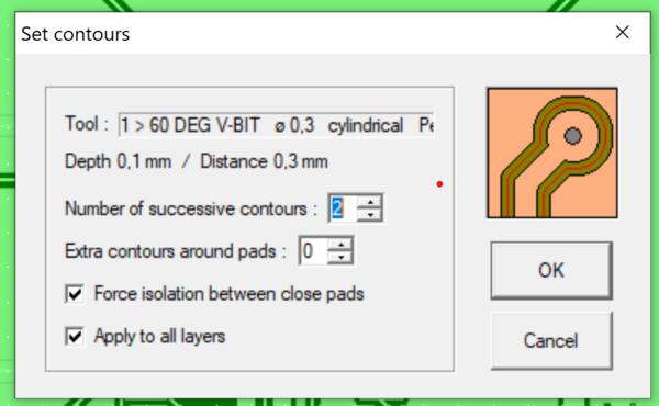
Next I clicked Calculate contours and now it shows that 60DEG V bit is used for isolation milling, and I got confirmed by lab assistant (and Gemini) that it's OK. I also set number of successive contours to 2 and extra contours around pads to 0 (to make the contours shallower than the previous ones printed here.) Also the other two options below are as supposed to.
I also heard that the engraving depth should be shallower than in it is at the moment, so I go to Tool Library and for V-bit I set Maximum depth per pass to 0.07mm. To make it update, I quess I have to start from beginning, which is quick because I have done it at least 5 times already. Well it didn't, so I set the depth in Selected tools instead.
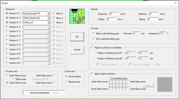
Then I'm ready to export toolpaths. I click Mill icon and check the sections, leave Mirror X unchecked and have the XY-zero point to South-West corner. Click OK and check that this resulted in two files for both engraving and cutting/drilling. Getting here took me almost 4 hours and I need to leave the lab now, so I continue the actual milling tomorrow.
Then I continued with preparing the milling machine and opened VPanel for SRM-20. Now I followed these Aalto wiki instructions.
In Vpanel I checked both coordinateds to G54, set spindle speed to one level down from maximum and in the setup I checked NC Code and unit millimeters.
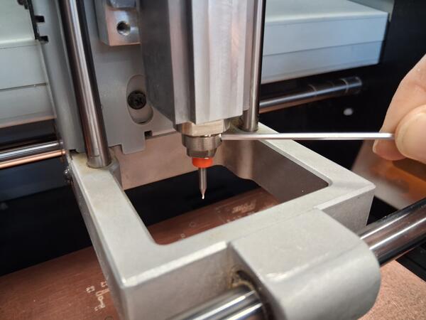
The board is already attached to the platform with double sided tape, so I install the V-bit to the machine, as the first step is the engraving. I pushed the bit as far as it got in the spindle and tightened it lightly. Then I set the Z-origin by moving the bit close to the surface, loosened the screw, let the bit to drop against the board surface, tightened again, and pressed top right Z on VPanel and Yes.
Then I set the X,Y-axis to the south-west corner of the (soon-to-be-printed) board, by moving the bit using the arrows on VPanel and pressing X/Y and Yes. The X, Y, Z, on the left are all now 0.00mm at the point where is the bottom left corner. Then I close the lid.
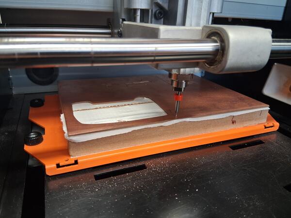
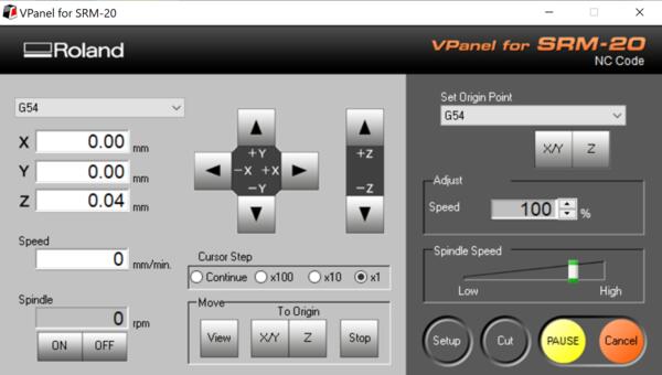
For importing the files to VPanel, I press Cut -> Add -> select the first file (T1.nc) I imported from CopperCam which corresponds the V-bit tool for engraving. (T2.nc is for cutting and drilling, i.e. the 0.8mm router bit.) Then I pressed Output and the machine started engraving.
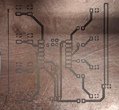
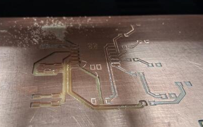
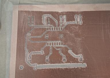
It took less than 10 minutes to finish the engraving. I vacuumed the dust away and now looking at the engraving, it is perfect near the orign but becomes too deep in the center and on the right. This is perhaps because the board is not exactly flat.
The lab assistant suggested that I do it again, now with even shallower depth. So I do the whole process from the start because coppercam doesn't open the imported .nc files and apparently I didn't save it in any other format. A good reminder of the CopperCam process (which I did yesterday many times). Now in CopperCam Parameters -> Selected tools... I set the depth for V-bit to 0.04mm. (Later I heard that you should not change the tool depth from 0.1mm)
Now I had to remove the board from the machine and double-tape a new one. The new board looks like it's been already refined out of the protective layer with a sandpaper so I don't need to do that. I place the board belly down on the platform. I started engraving but soon realized that my board does not fit on the board as the origin was too high on Y axis. Also now the engraving is too shallow or there was more egraving grounds to come. I don't have more time today to finish this.
Trying again, I begin with sandpapering the protective layer away. Using 0.04mm depth for engraving the print was still too deep and the traces between engraving were barely visible. I tried once more with 0.02mm depth. It became even worse. Below is the difference between 0.04mm and 0.02mm.
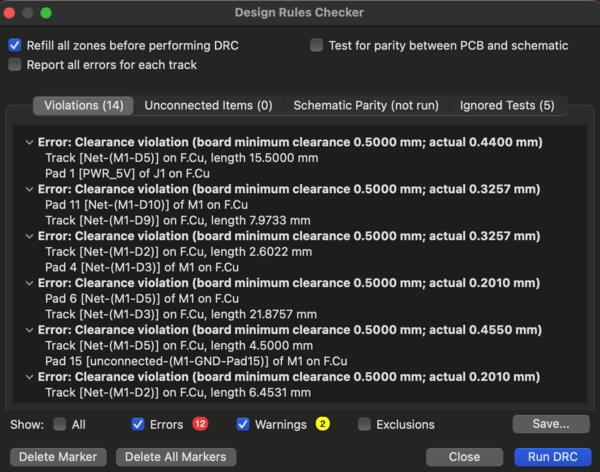
I figured that the problem is in the track width, so I went back to KiCad to widen the tracks. I didn't know how to do it so I asked Gemini about it. Finally ended up doing it in board setup and constraints and after that DRC showed a lot of errors.
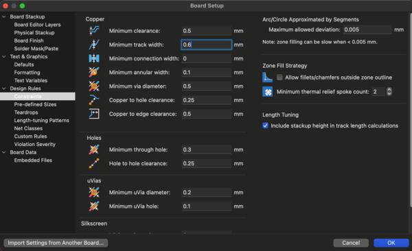
I rerouted all the tracks with wider width which was a pain in the ass. Only afterwards Gemini told that in the bottom right corner I can select only Tracks, pressed Cmd + A to select all tracks and pressed E to open Track and Via Properties. I set the width to 0.6mm.
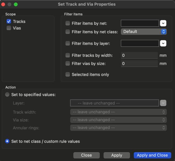
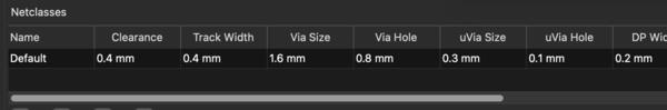
In a few minutes later my classmate came to ask what's up and I told what I had been doing, and he asked if I had done the net class configuration that Kris showed. I opened the menu and there was the track width 0.2mm while it should have been 0.4mm. So I had forgotten to do that in this specific iteration and that was the problem. Learning again. Now I set those values as instructed but left the tracks on the layout to 0.6mm anyways.
As DRC showed only two warnings on silkscreen layer, I ignored them, went back to CopperCam and went through the set up and started milling. The engraving wasn't deep enough and I remembered not having set the new depth to the engraving tool. I'm too forgetful because of feeling pressured to free up the workstation to other. So I canceled the milling and set the depth to 0.07mm and began again.
It still didn't seem to be deep enough so I paused it and back again to set the depth to 0.15mm. Still it didn't cut much further. one lab instrutor told me that you shouldn't toggle the depth and he did a trick of loosening and dropping the bit 0.04mm down from the Z-origin. And it's still really uneven. The problem now seems to be the really uneven platform.
And that's it for today as I had only a couple of hours time. The next day the unevennes was tried to be solved by having smaller boards to be cut from but I didn't try that out, but tried the other milling machine.
Bungard
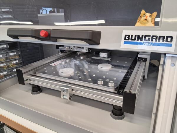
As Roland SRM-20 was reserved one morning, I began working on Bungard. It's a PCB milling machine for more advanced use with also more advanced configurations.
To begin with, I set in Kicad the net classes as instructed before, and set the track widths to 0.4mm. At first I followed the wiki for setting toolpaths for Bungard.
Tools are the same as before with Roland. I checked that the selected tools are as supposed to.
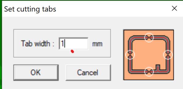
Added design tabs by hovering over layer 5, clicking layer 6 underneath it, right-clicking the outline and clicking Add cutting tabs: set it to 1mm, and place one to each side of the outline. These are for keeping the board in place when the outlines are being cut.
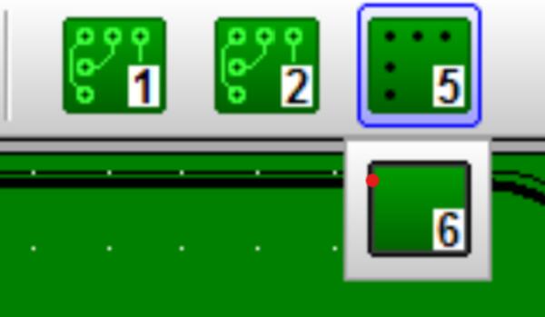
Selected the first layer and Calculated paths: set values as in the image (3 and 0).
Then I pressed Mill saved the files in .plt-format, and got two files for both of the tools.
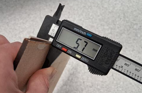
Then I moved on to the wiki for milling with Bungard. The thickness of the board was 1.6mm and the MDF board as sacrificial layer was 4.1mm.
As I had sandpapered the protective layer off the board, I taped it on the sacrificial layer. I need to take into account the different X and Y axises when placing the board on the platform, as my cutting board is not large enough to have my board printed on it tilted 90 degrees. The origin is on top left corner for the opening door, so if I want to think it in the same way as in Roland, I need to look the machine from the left side.
I removed the safety pin by pressing the know on top of the spindle and rotating it counter-clockwise. I checked with microscope that my V-bit is not broken and placed it in the colette as deep as it went.
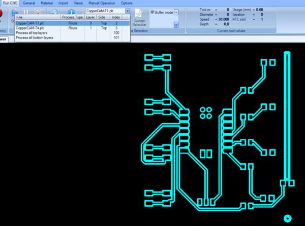
I opened the RoutePro3000 on the lab computer that is connected to Bungard. I pressed Wizard and opened a new project Wizard > Create > Printed Circuit Board; opened BOTH the T1 and T4-files (for engraving with V-bit); Side selection: Top; Processing type: Route and Material: FR4 (not really used); set parameters as shown in wiki for both files/tools. First it only opened the T4-file but doing it again I had both files opened. This was quite straightforward and I didn't take screenshot as my process looked the same is in the wiki mentioned before.
In the General tab, I set the Base thickness to 4.1mm, as I had calipered the MDF board, and in the Material tab I set Thickness to 1.6mm.
Then in manual operation with arrows I moved the spindle on top left corner of the board and set the origin there.
First it claimed that cabinet door was open, but it wasn't. After a few tries I realized that the bottom front red knob was stuck, so I pushed it a little to lock it and now it worked. When in place, I clicked Copy position to set the origin there.
On the Run CNC tab, I selected the first file (*T1.plt), clicked Start, and Ok, Ok.
The imprint looks so fine compared to my tries with Roland yesterday.
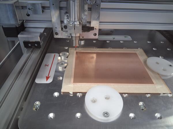
As the engraving was done I changed to bit to the router bit (checked that it's not broken.) Then on the Run CNC tab I changed the process to *T4.plt and checked that I hadn't forgotten anything. The other setting were the same as in the previous process. Then I just pressed Start (and Ok, Ok).Below can be seen a design tab in production.
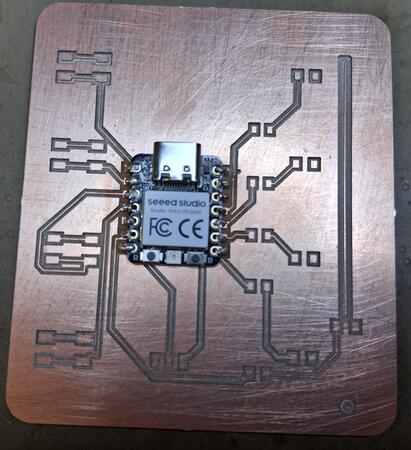
The outcome seems fine. I vacuumed the dust, detached the bit from the spindle, placed the safety bit back. Then I loosened the clamps, took the board out and closed the lid.
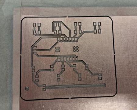
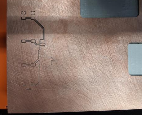
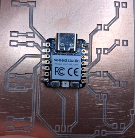
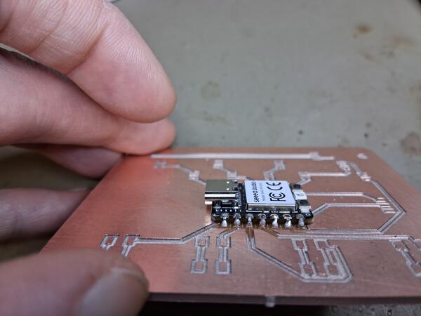
I used a small chisel to detach the board from the design tabs. Only now I realized that I hadn't set the track and the hole to be cutted through. Also I should have positioned the XIAO board to the edge of the board so that the USB is easier to plug in. Overall I'm happy that I finally got one PCB engraved and cut properly.
Electronics for my PCB
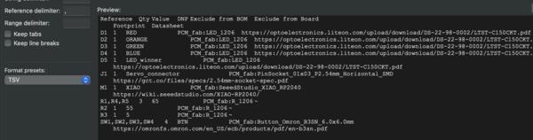
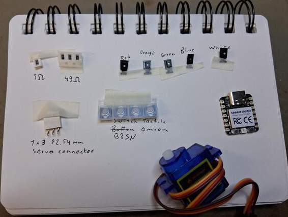
I began by opening the bill of materials on KiCad and collected the listed components.
I couldn't find Button Omron B3SN 6.0x6.0mm but I found Switch Tactile Omron B3SN (with same dimensions) and was wondering if they are the same or not. Asking a peer student and Gemini, it appears they are the same.
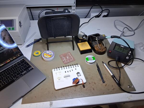
The soldering station was left partly assembled here and I only collected the solder, rosin, braid, solder sucker and tweezer. I wetted the sponge and turned on the soldering machine, the fan, and light. Then everything was set up.
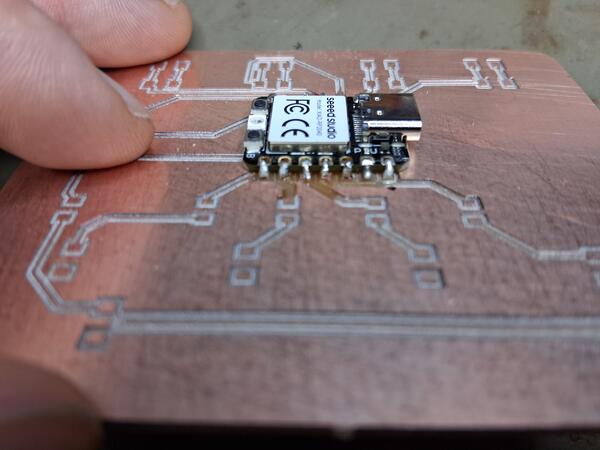
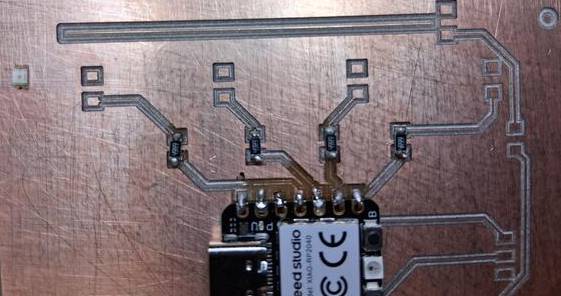
I began with the XIAO: soldered the opposite corners first to have it properly placed. It was quite annoying as no matter how much I tried to add the rosin, the solder seemed to want to run away from the board, sticking into everything else but that. This became easier over time and I also began to first add rosin and heat the spot well and then take more rosin and heat up before adding solder. As I had done all the pins, I looked over and improved a few of them. I can see slight burned area around each solder but hope they're all good now. Focusing on these tiny things is quite intense to my eyes: have to take a break before continuing.
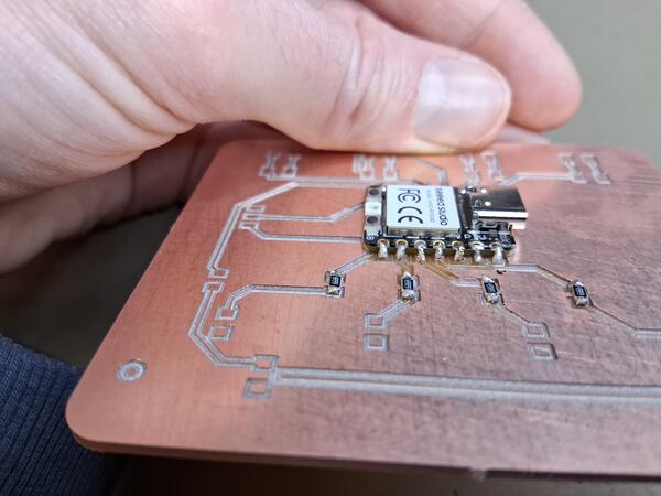
Now continuing to even tinyer parts: the resistors. As there was 50ohm (49.99ohm) resistors and 100ohm resistors, I decided to have the 50ohm for the three top LEDs and 5 ohm for the blue LED. Resistors don't have polarity so I don't need to worry about which way I place them on board. What comes to soldering these, I wish I had three arms: one for heater, one for solder and one for tweezers to hold it in place. I first placed the rosin on the spot, then tiny amount of solder, and then with tweezers and heater placed the resistor in place. Here I had to use the sucker once as I put too much solder in one place and it flowed over to the fill zone (ground).
As I continued to LEDs, I realized that the grounds are not connected to the fill zone as I had thought they were. It makes me wonder if the fill is connected to ground under the XIAO, i.e. it is not ground at all. This mistake has happened at some point in fixing the PCB layout at KiCad. What a bummer. I don't know if I should solder everything in place and connect the components to the fill zone with solder and hope that is ground. I don't have time to start over today anymore.
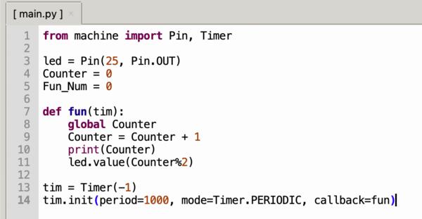
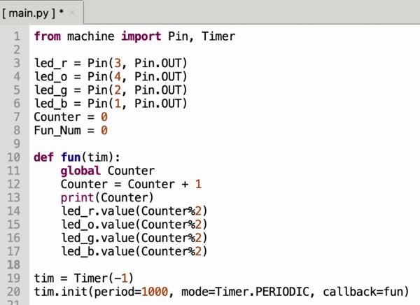
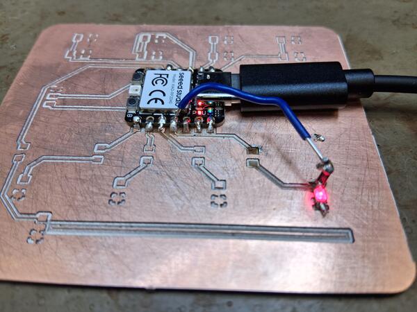
I decided to solder the red LED with solder flowing over to the fill and test if it works with the XIAO. To make the Blink test I returned to this micropython tutorial. I copied the simple blink test and changed the output pin to 11, which I checked from KiCad schematics.
Another student came to ask what's up and pointed out that I can just wire the fill zone to the ground. Why didn't I think of it even though I had just before recommended that to other student. There's still a lot of fixing and it can be easier to make another board.
Trying to make the LED blink, I'm having trouble with Thonny. First it said something about a problem with the interpreter, so I tried updating Micropython Raspberry Pi interpreter which got stuck in 17%. I canceled that and tried again and now it was stuck already at start.
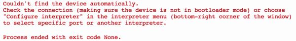
I close Thonny and tried reopen it and it didn't open. Restarted the computer and now it opens. It didn't work at first but when I tried the cu.debug-console port and installed micropython and reconnected the chip, there was USB port available, which I then selected.
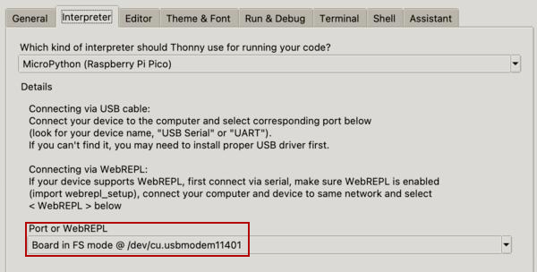
Now the LED blinks on the chip when port is 25 (integrated LED) but with port 11 nothing happens. I tried connecting the soldered LED to ground with a wire but still nothing happens. I had forgot to save the code to the microcontroller. I also checked the port from XIAO pin map and actually the port is 3 (middle one on the rigth) not 11 as in schematic. But still nothing happens.
Looking closely at the board, there seems to be disconnection on the track which has been burned by solder heater.
But testing connectivity with multimeter there is a connection between the resistor and the pin. Also resistance is shown to be around 50 between the pin and the LED "anode". But with the "cathode" end there's no connection. So maybe the fault is in the code...? Code works with the integrated LED, however, so seems weird. I tried connecting the LED ground directly to ground pin with a wire, nothing.
Now is the next day and testing again with multimeter. As the video below shows, the connection is lost with the LED. Thinking about this, I remember that LEDs need to be placed in right direction, which I had forgotten when soldering it. There's a tiny line on the LED indicating which end is the cathode.
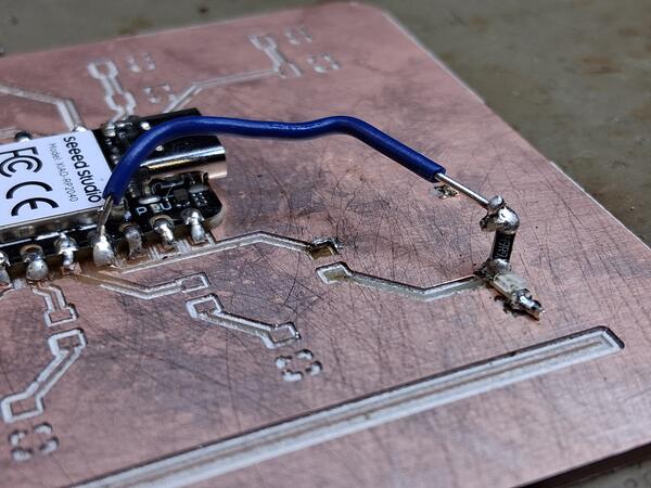
So I try swapping the LED. First nothing happens but then I remember that the fill zone is not likely connected to the XIAO ground, so I use a wire to ground it. And that works: now the code makes the LED blink. Yay! I solder the wire to the fill zone and ground, and also solder rest of the LEDs in right direction. I upgraded the code with all the pins (checked from pin map) to blink all the LEDs to test them. And it works.
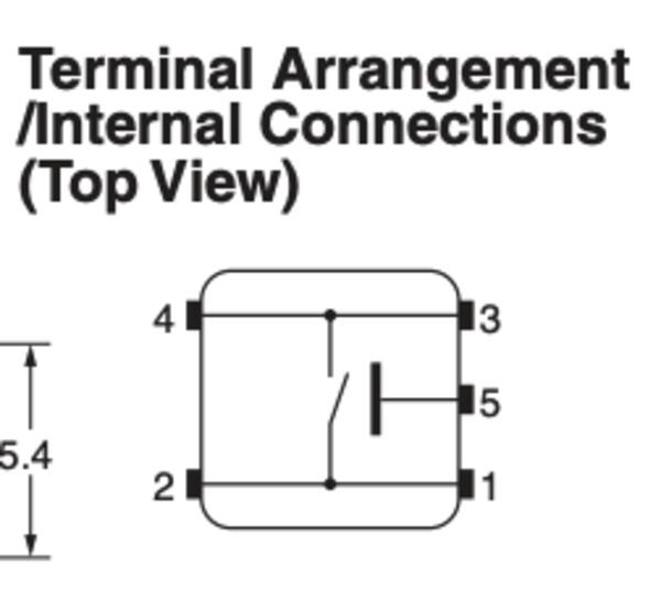
I'm not exactly sure in which direction the buttons/switches should be placed on the board. I asked about it from the lab instructor, and he showed that the siden on the button are actually slightly different and I need to check datasheet which is which. In KiCad Schematic editor, I search (A) omron switch and there I find link to the datasheet. This button is B3SN-3112P but I can't find any information on the markings on this data sheet and also Digikey has link to the same datasheet. I googled it and it says that from the bottom view when the text is upright the top right is 1, top left 2, bottom right 3, and bottom left 4. With the image below and thinking how the button works, there is no connection to ground when button is not pressed. As far as I understood, the pins 1 and 2 are connected to the XIAO board and 3 and 4 are connected to ground. I soldered one button and tested if pressing it gives input.
However, Thonny has again lost connection to the USB port, damn it. I tried restarting it and it doesn't work. I tried connecting in bootloader mode and it doesn't work. I'm afraid I broke the XIAO board because I began soldering the button while I had forgotten to unplug the board from computer. Google telling me this is likely the case, because soldering irons are grounded and connecting that to a pin caused a ground loop and fried the XIAO board. Damn it again. I guess I need to solder another XIAO if I want to continue. That creates unnecessary expenses, though.
It was quite difficult to get all the solder out from the pins, and when I finally got the chip out, it ripped some of tracks with it ruining the whole PCB.
Game over! Start again.
At least now I can fix the grounding issue on KiCad. I surrond the PCB with the tool Draw Fill Zones and then double-click and set Net to PWR_GND. Now I can see the grounds being connected to the fill zone.
I used Bungard again as Roland was in use. Only after starting the milling again, I remembered that the track hole could have also been cut through. Don't have time to think about it now.
Back soldering. I had quickly soldered the XIAO board on it's place and one LED, and then one resistor was misplaced and solder flowed to over the track to fill zone. As I was removing the solder and the resistor, it ripped the track with it and the PCB is ruined again. Now I give up.
*4 hours later* Well, I can use a wire to connect those. I'll do it tomorrow.
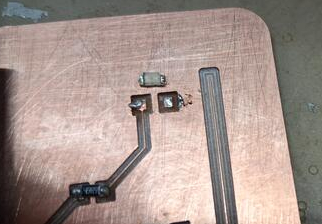
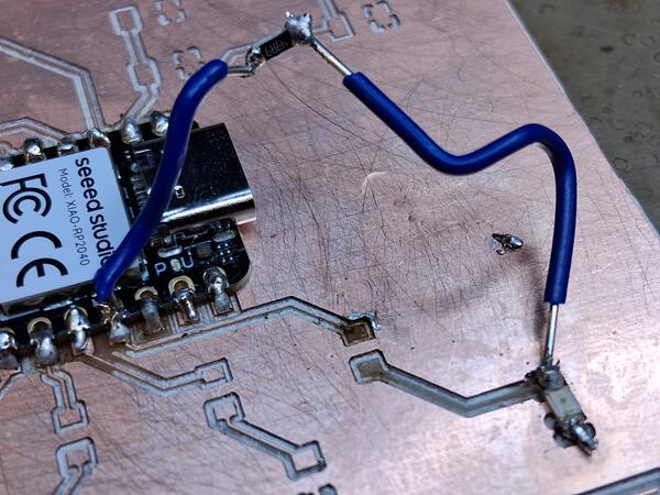
Back in the lab, I've now used over an hour to make the resistor soldered between two jumper wires: it is really frustrating. I could have done a new and better PCB in this time. Outcome is seen on the left, and it fell apart right when I touched it with a multimeter. Thinking about a better way, I came up with this solution and it is quite sturdy, and the led blinks.
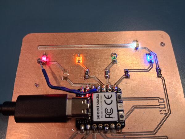
Soldering other LEDs and resistors is really annoying today, nothing seems to stick to it's place and the solder wants to flow over to the fill zone. Took many hours to get them in place (half an hour for the white LED) and then blue and white won't blink. I changed blue LED and that works. For the white I found out that the resistor is connected to fill zone. Fixing that and now every LED blink. However, later I realized that all the others but the red is upside down :E Got to fix that at some point.
The I soldered the first button and tested it: pressing it shows no change in it's value. Can't get any valua out of it with a multimeter: it might be also damaged from the soldering while connected to computer. I try solder another button to the next spot and test it. Now it shows default value as 1 instead 0 as the first button and does not react to pressing.
I anyway replace the first button with a new one and solder the rest of them as well. Testing: all the others, except the second one, react to pressing by showing the value as zero instead of 1, i.e. the ground is connected.
As I tested connectivity of the second button with a multimeter, it detects the state change when pressing, which means that the button should work and the problem is somewhere else (Same result when measured from the pin).
Well, I continue without one button, and the green corresponding led is quite dim being upside down anyways. So I test the code from the simulation with green one automatically correctly pressed. After some debugging with print commands to fix issues raised in importing the code from the Wokwi simulation and some tweaking (eg. added game over and win signaling lighting patterns), I was able to make it work. Game over signal is two seconds of every LED on.
To win, you need 40 correct hits (above video was 31) and the win signal looks like this: all LEDs blink one by one five times.