Electronics Production
This weeks task was to make and test a microcontroller development board that you designed
EDA software
EDA, or Electronics Design Automation, Software is what allowed for more complex boards to be made. Before them, just like most things in engineering, electronics boards were designed on paper. When EDA's came around, both the board and chip could be designed online. In essence, EDAs are the fusion 360/CAD software of board design.
Design
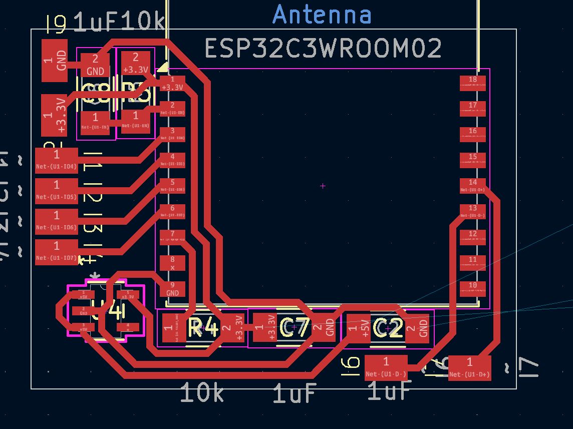
The design was pretty simple, as it is essentially my custom ESP32-C3 board. The main problems are that this is to be milled, and through testing I found that the milling machine had loads of struggle with just the voltage regulator I used, and therefore it would be absolutely impossible for it to mill a usb c port. This means that I had to design extra pads for usb C to be added in. Overall, the design was really easy, as it was just my custom board, but with all the usb c related stuff (the two 5.1k ohm resistors) taken off. I always say it, an I always will, the ESP32-C3, and especially the modules that have most components build in are absolutely insane for projects like this. the modules it comes in feature almost all of the required components, except for a couple small ones. Check the bill of materials to see just how useful using the modules are.
Schematic
The schematic was very simple, as it was almost exactly my old board, just pared down with the removal of usb c. I still even included it at first, in hopes that there was a way, but I refuse to attempt soldering a usb c unless if there is a soldermask. if you have experience with microcontrller design, you might look at it and wonder where a big part of microcontrollers are. This part is the USB to uart converter, that allows for communication between the microcontroller (UART) and your computer (USB). The great thing about the c3 is that its not needed, as pins 18 and 19 are USB d+ and USB d- thanks to espressifs clever design team putting one inside the chip. This means that the schematic you see below has full ability to communicate with a computer through only 4 connections
Also, I made a custom footprint for the esp32-c3, as I just find it easier to work with for projects like this. it clearly labels what needs to be put where, like the boot option pin, the usb pins, and the enable pin that aren't there on the default one but I always use them as that.
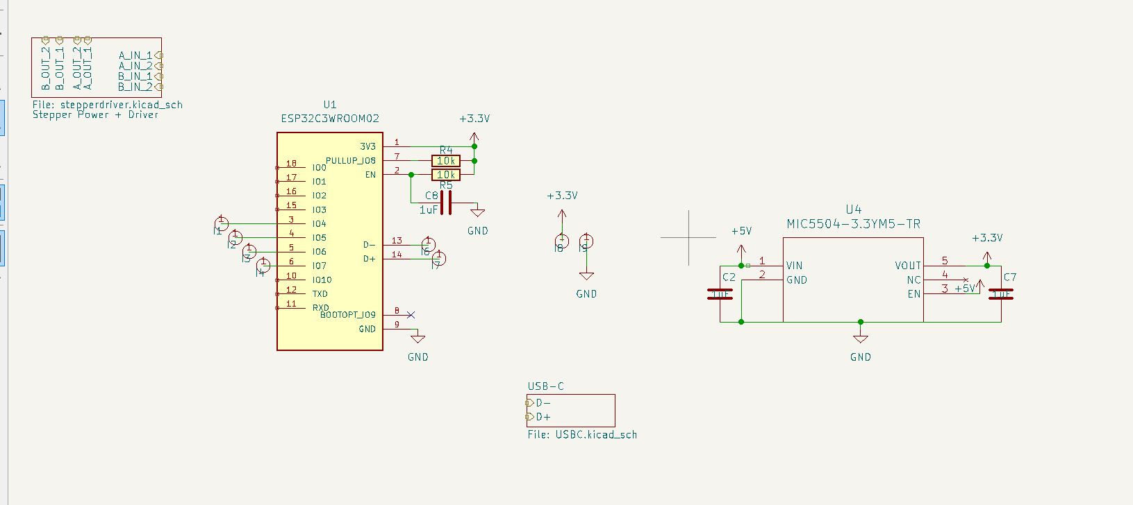 The other stuff in this design is for later weeks, as I partially worked on it so that it would be easier to add on later.
PCB
after figuring out what I wanted to put on it, I had to figure out where. As with the hx711 I made in electronics design week, I wanted it to be single sided and millable, and compact.
With all milled boards, trace width makes or breaks the board. Too small can result in a really hard time soldering or traces that fall off. Too bit traces will mean that you have to space components much farther away, which is an issue I ran into with this board.
I also had the idea of used castellated edges, so that I could solder this directly to my stepper driver (coming soon) and the battery charger (also coming soon). In the end for those, however, I ran out of time as my fab was closing for our schools spring break, and therefore just had to solder the pads on it board. looking back onto it, this kinda sucked, but it works for now and I will definitely be remaking this once I know the final goal.
Because of that, the placement of the pads was kind of an afterthought and its visible in my power and ground being on the opposite side as the data pins. This will be fixed in the final, but I was on a time crunch so thats just the way it is.
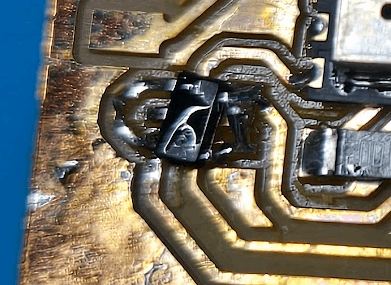
Laying out the PCB was fun, as it always it, except for the voltage regulator. I put it in a fine place, but the way I placed it required a trace to be routed through the middle of it. When going to mill, this trace was the death of me as It was nearly impossible to get it to not bridge at some place while still being thick enough, but I eventually got it working
The 4 pads are for the stepper, but I really don't want to have to solder them without bridging, so im going to make them castellated and cut them again after the lab reopens.
Bill of Materials
| Component Type | Part Number | Quantity | Package Type | Description |
|---|---|---|---|---|
| Resistor | 1206 10kΩ Resistor | 2 | 1206 | |
| Capacitor | 1uF Ceramic Capacitor | 3 | 1206 | |
| Voltage Regulator | RT9080-33GJ5 | 1 | SOT-23-5 | Drops 5V from USB-C down to 3.3V |
| Microcontroller | ESP32-C3 WROOM-02 | 1 | N/A | a really solid microcontroller. not the bare ic, but a much better version for all but the smallest projects |
As with most electronics sourced from a place like digikey, it is usually better to buy a lot vs a few. I highly recommend doing that here, even for the voltage regulator, as im pretty certain that it is the best price/max current ratio available at its small size.
Fabricating
Just like the shopbot, I am a hater of all milling machines. They just always mess up on me somehow. However, I lost my mistrust of the shopbot when using it last week, and I lost my hate of the milling machine this week. Just like the shopbot, I have pervious experience on it, but that was making a single led and resistor circuit, and I had a very streamlined usage of the machine, which still ended up in really thin unsolderable traces. This time, I used the best bit I could use without having to switch bits to drill holes (1/64 inch). This is the standard in my lab, and for god reason. It comfortably allows for .4-.5 trace width while still not making stuff look too spaced out.
Preparation
Physical
As I was the first one to turn on the machine, I had to set it up. Here, Andrew Puky helped alot with setting up my machine. The machine I used also had something messed up, where the auto touch off didn't work unless a alligator clip was grounding the bit. This was pretty easy to fix, as our lab had a giant warning on it, but was still scary. Besides for that, I just loaded in the bit, homed the machine, and taped up the copper and placed in our labs jig. Very easy setup, not as scary as I remembered it, but thats mostly thanks to Puky's great help
File
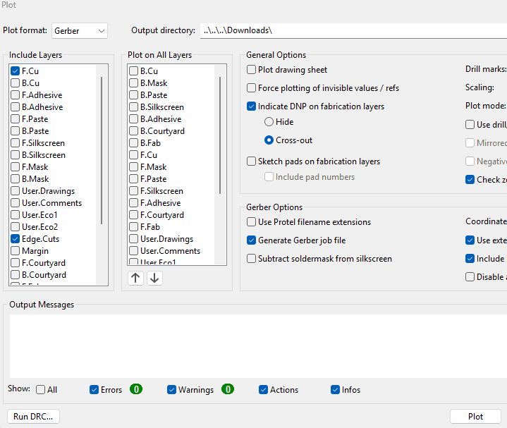 I had to get my file from kicad into othermill. This was very easy, as I Just had to do fabrication outputs, exporting the gerbers of the edge cuts and f.Cu. After doing that, If you were using drill holes (I wasn't) then you would also have to generate the drill files. After getting the files, I prepared them and sent them into othermill
Bantam Tools
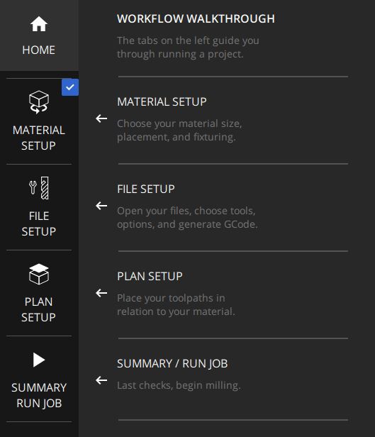 Honestly good software. Usually im like angry at all the software for the machines as its usually not the best, but this is a very streamlined software. to use it, you just go through the stages, visible on the right.
In material setup, you define the "stock" you are using, in this case copper sheets. As we have a jig, we dont have to worry about x or y. Z is important though, as the machine needs to know how thick your material is to cut through. For our lab, generally 1.7mm is our sheets, but its always good to check with a caliper before taping down. I might of forgotten, but the copper sheet I used already had a cut out of it from the machine I was next to, and it worked out for me, just its not advisable to do this.
File setup is where you import your file, this means loading the f.cu, then loading the edge cuts. Also, load in the PTH file if you are using a drill
Plan setup is where you define the bit you are using. The machine reminds you, so its hard to forget, which is another win for this software. Also here is where you define the offset for your cut. This is important for my cut, as the default place (bottom left corner) already had a cut in it, so I had to use the offset to position more in the middle
File Issues
As I talked about earlier, the voltage regulator was horrible to work with on this. The way I setup the board, I had a trace going between its two pads. Combined with a 1/64 inch bit, this was really hard to make work. The first thought I had was this
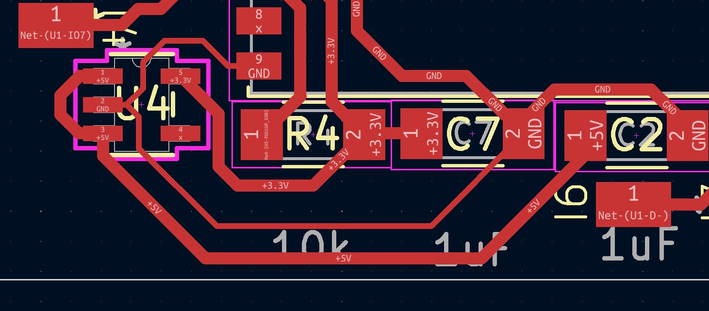
As you can see, it is not an optimal solution, but it was a solution I used for the first board
Milling
After getting all the files and machine set up, I just had to press a button to make it mill. It cut perfectly, and took only around 3 minutes.
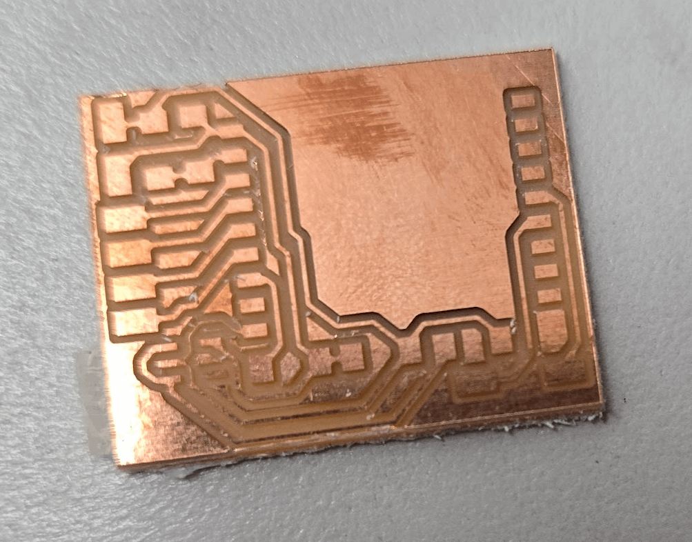 This has a SMALL issue, that being the small trace under the board. In order to fix this, I changed the board so that the trace was barely thin enough, but it still worked and was the best I could do. This all was milled on thursday afternoon, with the lab closing on friday afternoon, so I was really facing the time crunch then.
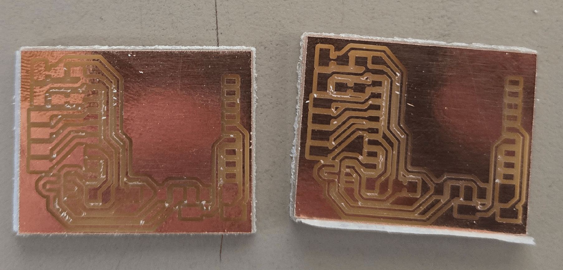
After making and fixing the issue of the first, I made 2 more with a wider trace. The 1st of the two did have a bridge, but I was able to just cut it with a utility knife as it was so thin
Soldering
Solder Stencil
Heres something im really proud of. Inspired by the urge to not pay for one, combined with my hand being shaky enough to want one, ive looked for a while for another way to make stencils. After a lot of testing stuff, I found a really useful method. Using a laser cutter, I was able to cut out the f.paste and edge cuts layer in paper. I used print to pdf from kicad, and then took it into coreldraw, here I set up the file for engraving, making the width of all the lines .75 inch so that the outer line (edge cuts) cut fully through. Through a lot of testing, I found that engraving was able to not set my paper (and cutter) on fire, and also resulted in cleaner cuts than a really slow and low power cut. The optimal settings i found were 100 speed, 10 frequency, and 50-70 power (depending on the paper thickness) I also found that a lower power and multiple passes was more clean than a higher power one, but it is a speed tradeoff.
Heres where I messed up, as I also cut out the pads that I didn't intend to solder at the time. This meant that when going to use the heat plate, I had to cover all of the pads with tape
Heat plate
In order to use the stencil, I like using electrical tape on every point I can to hold the paper as tight as possible.
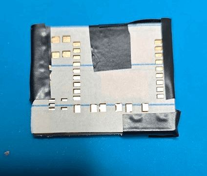
As always, great results from a stencil that cost the same as the same as a piece of dust.
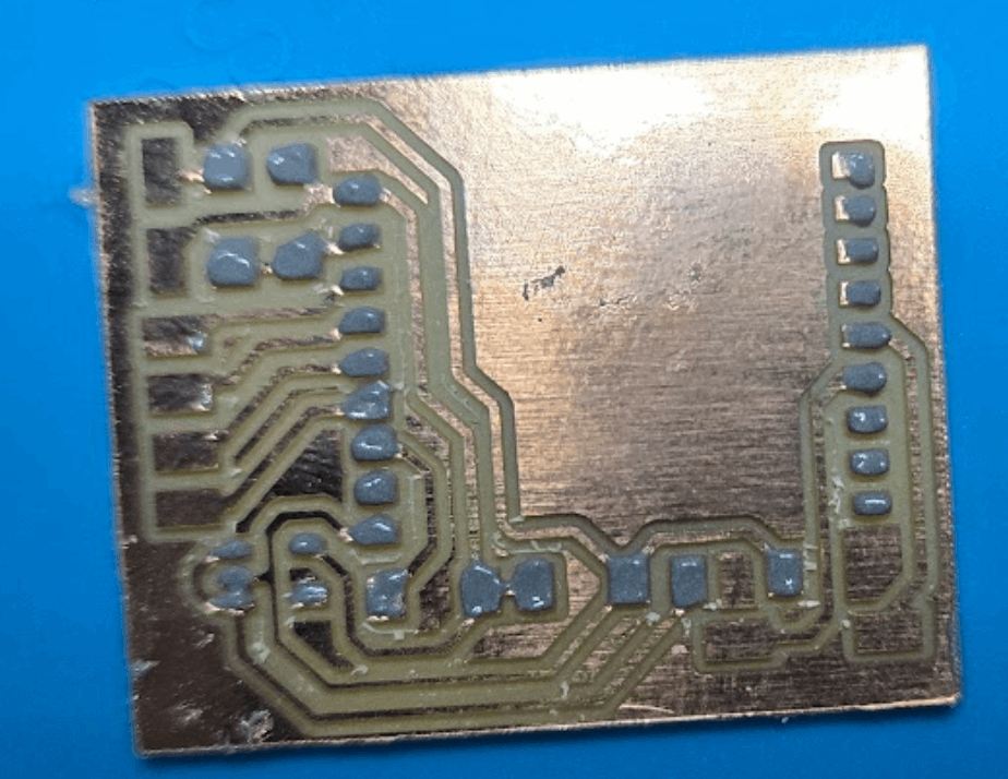
After getting the solder on, I put on all the components
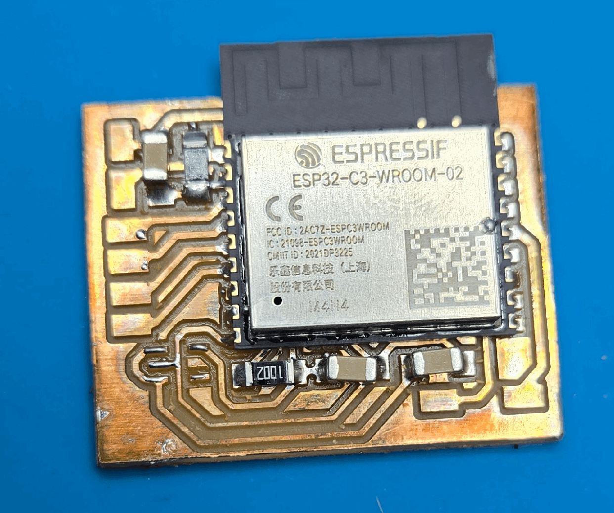
That voltage regulator again
If you look at that image, you might see something missing. Here again, its the voltage regulator, as it didn't line up well on the hot plate and I had to attempt to hand solder it. Heres where I hate a milled board, as this was horrible to get working, but it somehow worked even when it looked like it absolutely should not.
Pads
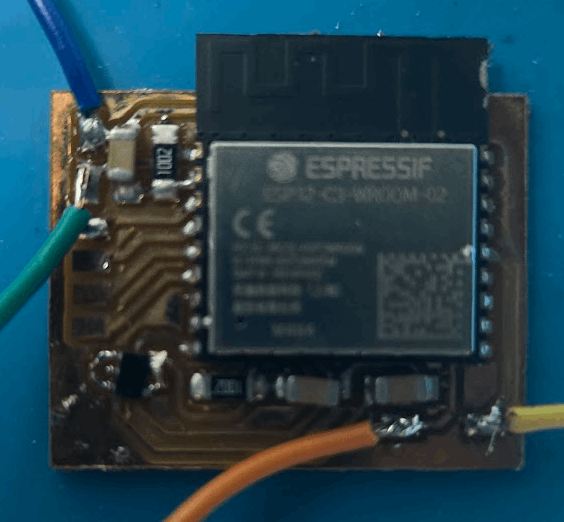
the pads that I put in in order to make in time also messed me up, as I had to solder them. Again, hand soldering on copper boards are my downfall. I got it working, but it ruined the perfection of the board that came before hand soldering, and I hope to be able to avoid in the future.
How does it work
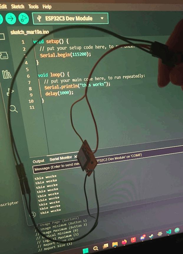
I have absolutely no clue how it works, some issue somewhere should of defiantly messed it up, but it worked and im not complaining. Actual miracle, as Im looking back on it and im just putting 5v into the pin. As all of my esp32-c3 boards, it does do the connect/disconnect loop when I first connect it, but after flashing anything it fixes it. I also had to make sure to turn on usb cdc on boot, as I am using the built in USB and without it serial does not work.
Reflection
Coming off week 7, this week aligned more with what I actually want to do in college and as a job. It has sort of set in stone that my dream is to design pcbs for rapid protyping
I don't hate milling machines anymore
overall, they were very pleasant to work with, which is kind of the reason that I made 3 of my board when I only ended up needing the first. I don't hate them anymore, but I do want to try and take the laser cutting further and use chemical etching to make boards in the future, Ive ordered ferric chloride (and probably been put on a watchlist) and hope to etch a pcb by the end of fab academy
I need to design better
all of my issues related to soldering can be tracked back to me designing bad, especially the pad. I can mostly blame time, as I feel like the voltage regulator could also have had modifications in order to have it work. Essentially, I need to make traces as big as possible, place stuff in places where it is as easy to solder as possible, and probably just use standard through hole instead of whatever I was trying here.
Group Work
A link to my group work can be found here
For my group, I described how to submit a board to a board house, a copy can be found below
Submitting a PCB design to a board house
What
Submitting a PCB design to a board house involves preparing and sending your design files for professional fabrication. This typically includes Gerber files, drill files, a bill of materials (BOM), and any special instructions for manufacturing. The board house handles processes such as etching, drilling, applying solder mask, and adding silkscreen text.
Why
Using a board house ensures higher quality, precision, and reliability compared to in-house fabrication methods like PCB milling. Professional fabrication offers:
- Multilayer designs: No more being tied down by being unable to cross traces, a board house and vias allow for thinking in 3d
- Multiple boards at once: The minimum for almost every boardhouse
- Tighter Tolerances: Achieve finer trace widths and spacing than most DIY methods.
- Solder Mask and Silkscreen: Professionally applied for durability and readability, soldering is 10x easier
- Consistency and Scalability: Ideal for batch production, ensuring each board meets the same quality standards.
- Panelization: making multiple PCBs on one board, really cheap batch production with a proper design
- Silk Screens: You can print graphics on the board, impossible with a milling machine alone
- Solder Mask: You can cover up the traces you don't want to solder, would be incredibly helpful when milling
Design Considerations (for JLCPCB)
If using JLCPCB as your board house, keep the following in mind:
- Board Dimensions: JLCPCB supports large sizes, and boards from 10x10mm to 100x100mm cost the same, almost every board will be within this size
- Layer Count: Supports 1- to 6-layer PCBs. More layers increase cost and complexity, generally 2 works for anything, with 4 allowing a power and ground plane ontop of 2 data planes, 4 layers stay pretty cheap, but above that adds great cost
- Material: Default is FR4 (1.6mm thickness), but 1.0mm, 1.2mm, 1.4mm add no additional cost
- Copper Thickness: Standard is 1oz ; 2oz is available for high-current applications.
- Minimum Trace/Space: 0.152mm is the standard minimum. way better than a milling machine
- They make the boards in china, so keep in mind for very rapid prototyping that for where we are located (US east cost) that our 8am (when we would expect the boards to start being produced) is exactly when they stop making boards for the day. Essentially, submit a board later in the day for it to go into production quicker
How
Assuming you are ordering from JLCPCB, It is highly suggested to install the Fabrication Toolkit. This plugin allows for a single click to export your board, with the right settings, for JLCPCB production. To install it, follow their guide
After installing the plugin, restart Kicad and then go to the finished PCB design you want made. On that page, in the middle of the top bar, there will now be a button that looks like this 
Once you click that button, a menu will pop up. For purposes not involving PCB manufacturing in the board house, no settings need to be changed.
After generating the files, go find the folder, called "Production". Inside that folder, there will be a zip, which is the only thing you need for just PCB ordering.
With that zip, go onto JLCPCBs website. On the website, find the add gerbers option

It will prompt for a zip file, and load in the file in the production folder.
After waiting a bit(10-20s) for the file to be processed, you can start to change settings for your board. As long as it passed the design rules checker, there will be no required additional costs, which will mean your board is either 2$ if theres a special offer(there almost always is) or 5$ with no savings.
There are some settings that you can change without any downside, for example the thickness, which can be anywhere from 1.0 to 1.6mm without a price increase. You can also change the color of the soldermask without additional cost, although it will take more time to make.
JLCPCB is also really good for cheap prototyping as it is the only major board house that offers a really cheap shipping, with the global standard direct line being around 1.50$, although it takes around double the time of the next fastest option (8-12 days, usually exactly 8).
After adding the board to your cart, select the board and then check out.
Receiving
During checkout, you pay and if you dont make an account, say where you want it delivered. There is virtually no benefit to having an account except for a purchase history, so it is not necessary. The box will be a blue box marked with their logo, very visible, and pretty alluring to package thieves if that is an issue in your area.
Design Files
All design files can be found here
Ignore the naming, this board is part of a stepper driver and therefore is named as such, Also there are artifacts such as the battery and stepper driver ic in the design, just ignore them or find them cool
The stencil is fixed to not have the pads on it, which will make solder pasting easier
