Electronics Design
This week's task was to
use an EDA tool to design a development board that uses parts from the inventory
to interact and communicate with an embedded microcontroller
      extra credit: try another design workflow
      extra credit: design a case for it
and as a group
use the test equipment in your lab to observe the operation of a microcontroller circuit board
Design
Design Goals
I like to think that I have more experience than most people, especially in kicad, so I hoped to achieve both extra credit goals. What I hoped to build was a way to easily interface my personal esp32-c3 microcontroller with a hx711 load cell IC. while my lab did not have any hx711, I had ordered them earlier as I am working on a different project that involves 2 scales, and really didn't like the amount of connections required between 2 hx711 boards purchased off amazon.
looking online, I found that this amazon listing that contained an image of the board design. This was corroborated by the references at the bottom of this sparkfun article, that included how design files for eagle and another circuit diagram with some features I didn't need.
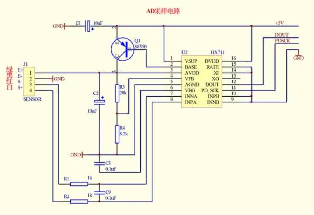
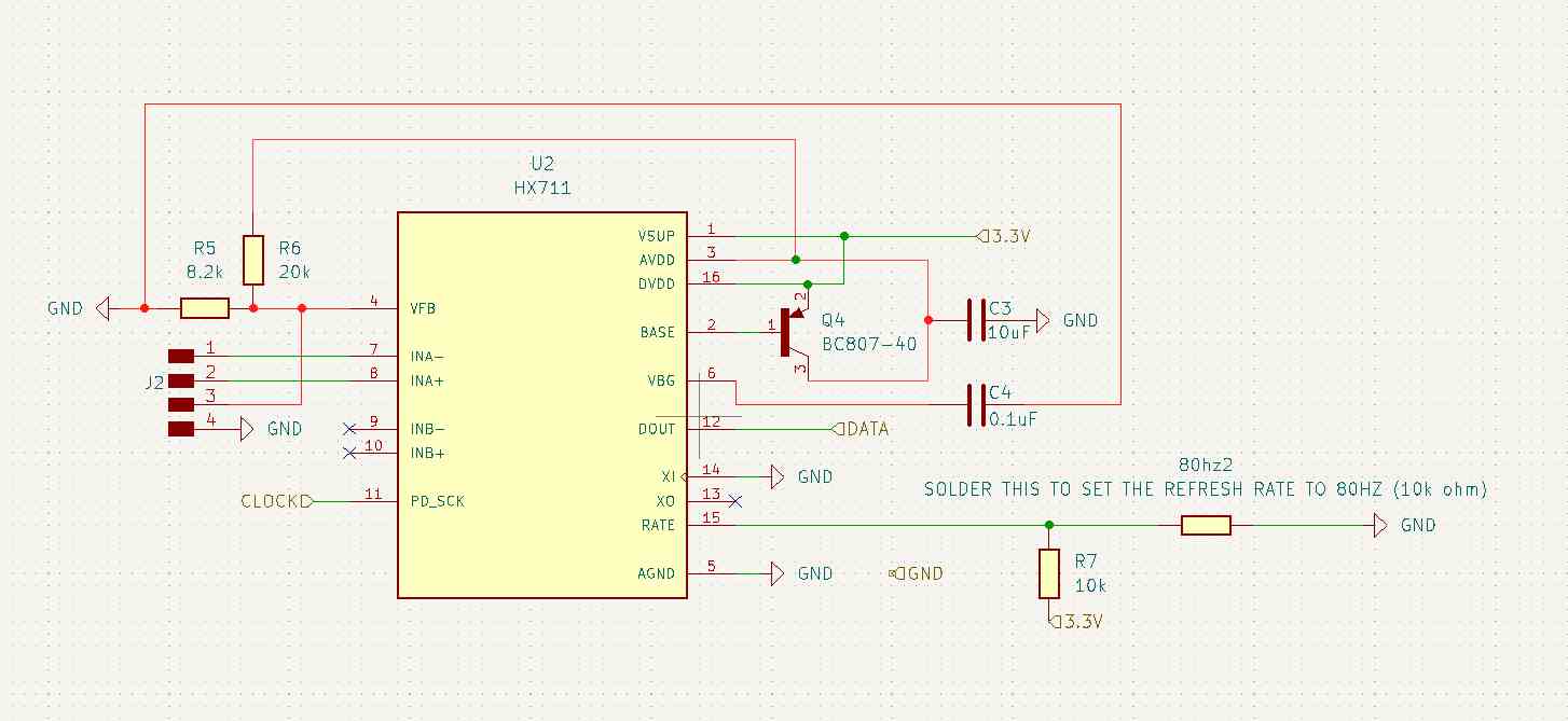
Looking deeper, I found this image that included no extra components, which I would base my design off of. I did notice that the sparkfun board defined the values of R1 and R2, so I would combine the two designs to get what my design would look like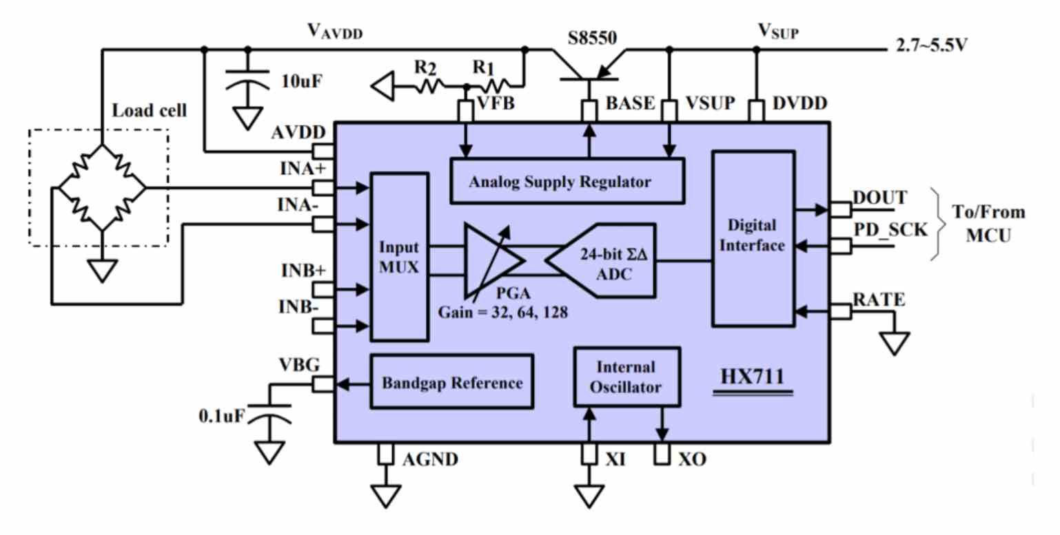
Why Design This
I already have 2 separating working hx711 boards. But I want to have 2 scales wired up to one microcontroller, which causes me to need 16 total wires, 8 from the microcontroller to the hx711s, and 8 more from the hx711 to the scales.
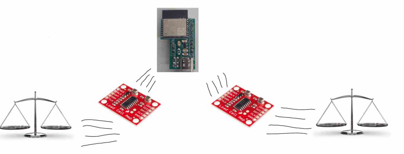
I want it to be like this, where the hx711 and microcontroller are soldered together, so that I only need half the wires risking getting caught on stuff
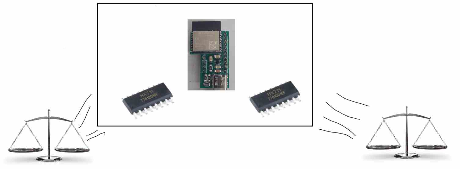
While these sketches aren't that good, every wire drawn on them is a physical wire that I would have to wire in real life, and I dont want to have to do 16 wires.
EDA's
an EDA, or Electronics Design Automation software is used to design, develop, and test electronic systems such as PCBs.
Choosing an EDA
for me, the choice is between Eagle and Kicad. They both have their advantages, which I get into right below, but its generally professional solution vs open source labor of love.
Kicad advantages
- Free
- Cross Platform - native arm64 build for windows, a big drive for me using it
- highly customizable - I use a theme that was built for OLED screens, and it actually does go a long way to save battery
- open source
- preformant - compared to eagle, kicad was made just for PCB and doesn't have the extra features eagle has as a part of fusion
Eagle advantages
- Intuitive Interface
- Fusion360 integration - easily put a 3d model of a PCB into a design
- easy component library - really easy to find and import footprints and schematics in app
- Bugs are nonexistent - while Kicad also rarely has bugs (it has crashed a single time on me)
Why I choose Kicad
I use kicad because
1. I have used it before, in my engineering classes it was what was taught to use and I kept using it after that
2. Its free
3. Its has a build for windows on arm
General and simplified workflow with Kicad
Below this section is the full workflow I followed while designing, but heres a general workflow for starting a design. 1. Find Parts you want - For this I use digikey for the actual part, and then octopart to find the footprint of that part 2. Import the parts - Here you take what you want, and import its schematic into your EDA, using what you found on octopart/digikey 3. Follow Datasheets - For any board using an IC chip itself and not a board like a xiao, you HAVE to consider the datasheet while designing. Basically every datasheet has something similar to a "application diagram" which outlines exactly how the PCB should be designed and wired. 4. Consider use cases - While following that datasheet, consider how your board will be used. If its going to be milled, increase the trace width and avoid vias. If it is going to be ordered, make sure you are following the specifications outlined by the board house 5. Use Examples - After your board is fully designed, compare it again against the example in the datasheet or other examples you can find online. Usually, they have a very good reason for placing it at that specific placement, for example the antenna on my board must overhang over the copper
Installing Kicad
While I already had kicad installed, version 9 was released as this week was starting, so I decided to update to it. Kicad is a blessed software as it has a native arm64 build which makes installing it 20x easier. After downloading the 1gb file from their website, I only needed to run the installer. The only thing I did different was to make sure to tell kicad that I wanted to import the library files from kicad 8, which was my previous version
Finding Footprints and Symbols
Part of this assignment is using parts from the fab inventory. While the hx711 is not a standard part, I wanted to make sure every other part was.
HX711 symbol/ importing symbols and footprints into kicad
For this project, I needed a symbol and footprint for the HX711 I had, which was a SOP16 package. The easiest way to find a specific chip's files is on snapeda, which is essentially an inventory of all the different symbol formats. The only problem with snapeda is that it requires an account to use, but it just makes finding parts so much easier that it is worth it
Fab Academy Kicad Library
The easiest way to find parts that your fab lab has is to use the kicad fab library and the fab inventory. Using the fab inventory to find a part that works and then being able to put it onto a schemative because all parts are in the kicad fab library saved me from having to go onto snapeda and find the individual part there
Importing symbols & footprints into kicad
 Importing symbols into kicad is easy, but you need to make sure you do some things before evening opening kicad. One big thing I always do is save the files to somewhere they wont be deleted, which for me is inside my onedrive. Once they are in a safe place, all you need to do is open kicad, navigate to preferences -> manage symbol libraries, and click on the folder icon near the bottom of the page that opens up
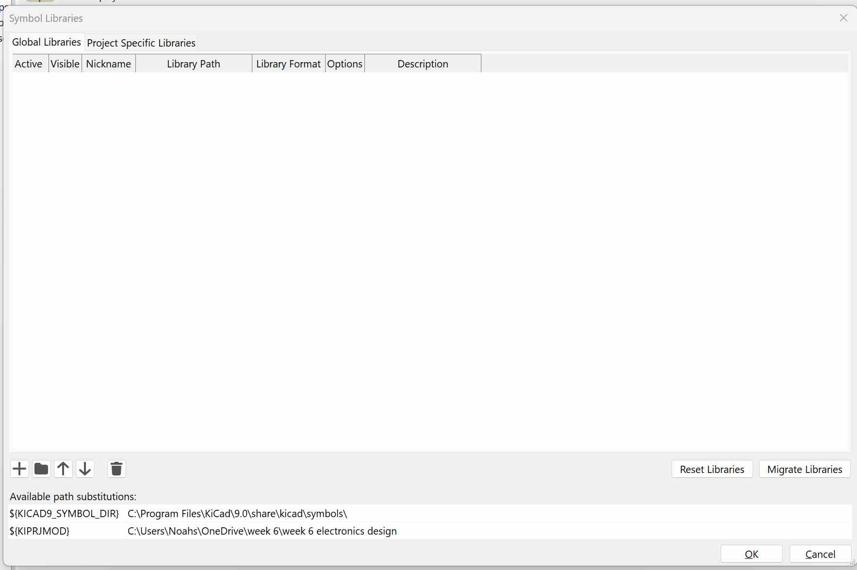 once it opens your file browser, open navigate to where you saved the file, and load in the symbol file, which will almost always be a .sym or .bak for an individual file, or a folder of .sym or .bak for multiple at the same time
for importing footprints, it is the exact same procedure, except that you need to go to navigate to preferences -> manage footprint libraries, and then find the files that are folders, and often have names that end in .pretty
HX711
before even worrying about my microcontroller, I needed to get a hx711 with proper design. After getting all the schematics and footprints I needed, I wanted to start on making the board. I decided to recreate exactly what was shown in the reference image, and then modify it to work with my custom esp32-c3 microcontroller. I started by figuring out which parts my lab had, and I found a sot-23 transistor that would work perfect in place of the s8550.
Hierarchical sheets
In Kicad, by default you have the "main sheet". just like github, you can create branches off this sheet, called hierarchical sheets, in order to avoid clutter, easily duplicate, and easily edit. I used a hierarchical sheet for my hx711 board, as I planned to use 2 of them, and the sheet greatly helped my final design look much cleaner. In order to make your own, I would suggest looking through this post on the kicad forums
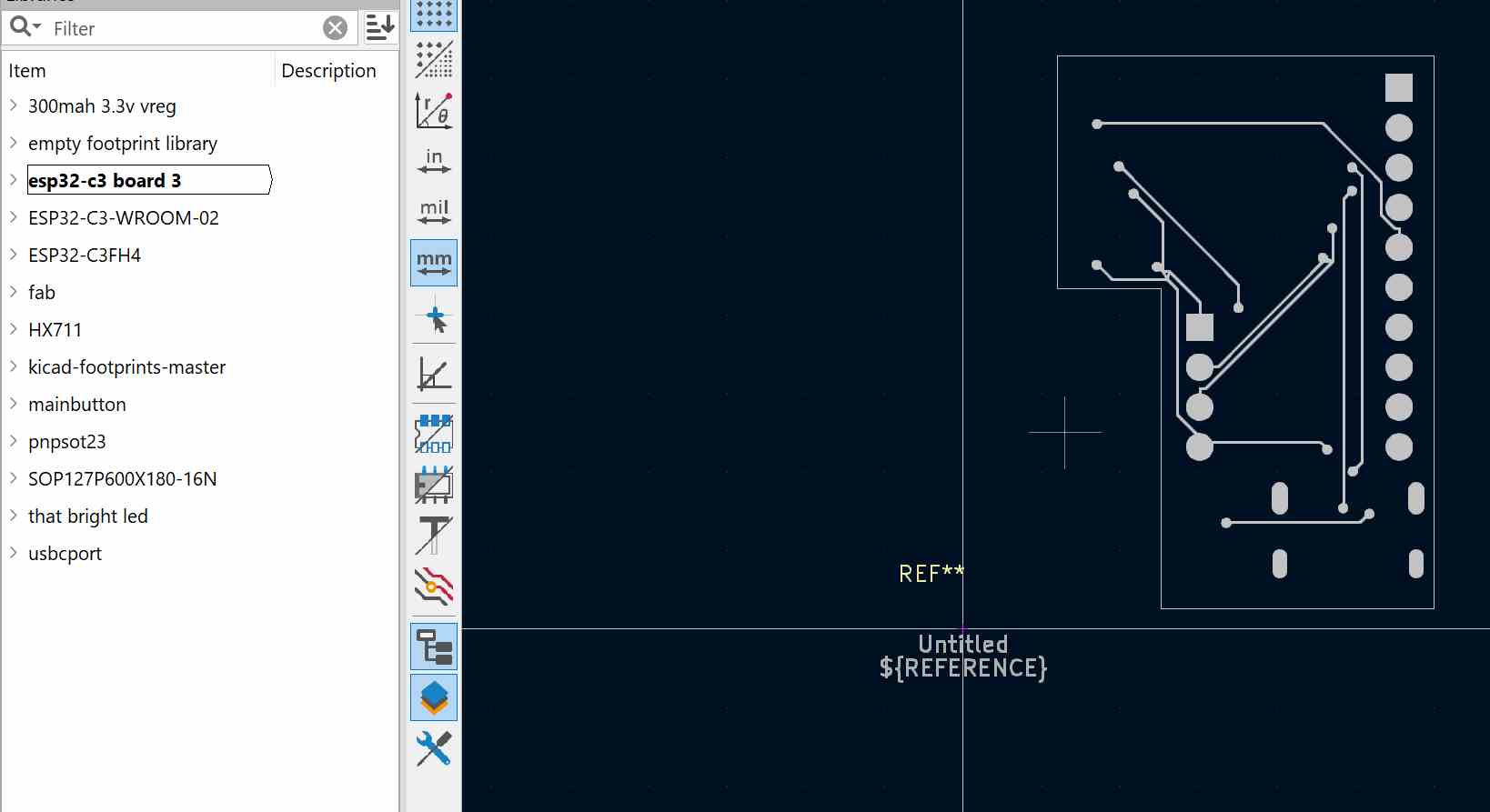
 After finishing the design of the hx711 portion, I needed to assign footprints. Kicad makes it very easy, and all of my footprints except for the transistor and hx711 were already assigned thanks to kicad's auto footprint association feature. In order to find the footprint I want to assign, I had to type in keywords, for example hx711 for the hx711 and sot23 for the transistor, because its package (shape) was a sot-23
Heres what the footprint assignment tool looked like for the hx711 board by itself

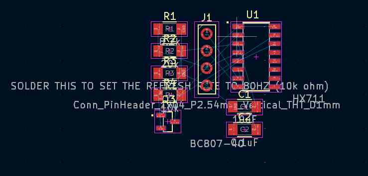
Heres what it looks like once the footprints are imported onto kicad's layout designer
Footprint & Symbol Design
I have never used the microcontroller I made for directly soldering onto a board, I usually use it with a breadboard, and therefore I needed to make a custom footprint and symbol of the board.
Footprint
Because of the fact that I have no experience in footprint design, I learned from this youtube video and this sparkfun article. Thanks to these, I knew that the easiest way to was to export the microcontroller board as an svg with only its back and edge cuts so the edges were visible, which gave me this.
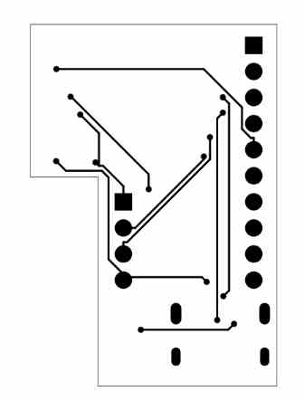
After getting the board's svg, I went into the footprint editor in kicad, and created a new footprint. After creating this new footprint, I imported a graphics object of the svg I had just gotten
After getting the svg into kicad, I started playing around with pads in order to make the through hole components. I found that a .8mm hole in a 1.6mm pad allowed me to easily place the pads while still keeping them big.
Finalizing Schematic
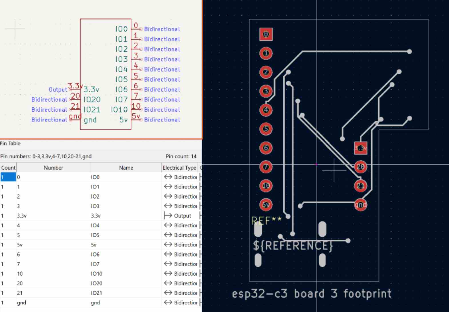
After making the physical design, I went into kicad's symbol editor and created the symbol, following this guide. I made the symbol look as close to the physical board as possible, with those pins being labeled how they are referenced in code, or what they do for the power pins.
Connecting
After finishing the symbol, I needed to assign pads. Pads are basically what allow the footprint and symbol to interact, like for example on the image below, I would assign the pad 3.3v to both the top left pin on the symbol design, and the top right pin on the footprint design, which connected them and allows kicad to know that this pin on the symbol is the same pin as this one on the design, and it should be routed as such
Finalizing Schematic
Before starting the pcb design, I needed to connect the microcontroller to the hx711s, Using the heriarchical sheets made this very easy, and all I needed to do was define the heriarchical pins, which are basically how a component not in the sheet can interact with the sheet. I then placed 2 of the sheets onto the main design, and defined the pins there so that they linked up. I also added in 4 pins on the left side, which are the tx and rx pins of the esp32-c3. I designed the module so that it would be very easy to add in tx and rx breakout, and so I said why not and added them in. My final schematic is below
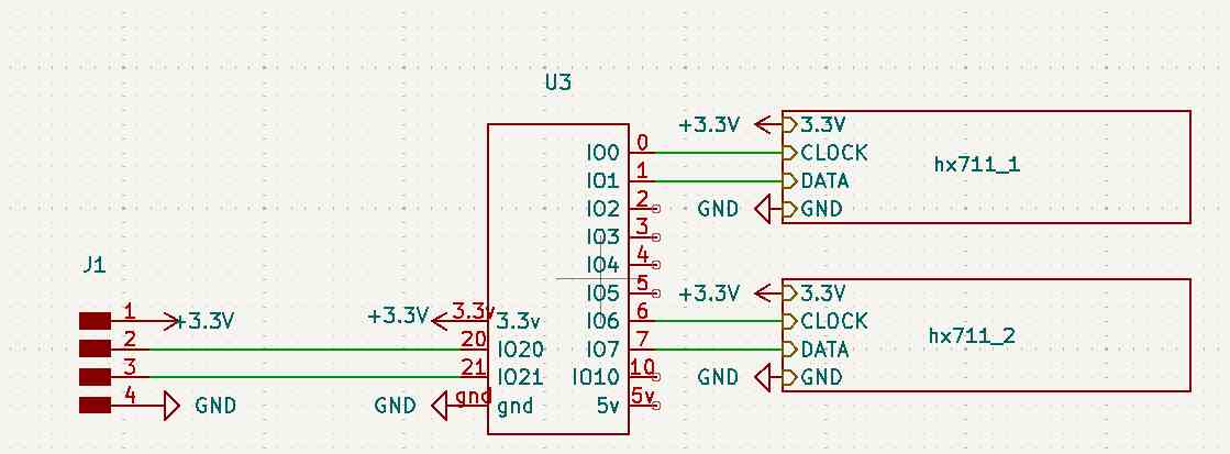
PCB design
What I wanted from the pcb was a millable board with a hx711 and its 4 pins on each side of a microcontroller
Plugin Problems
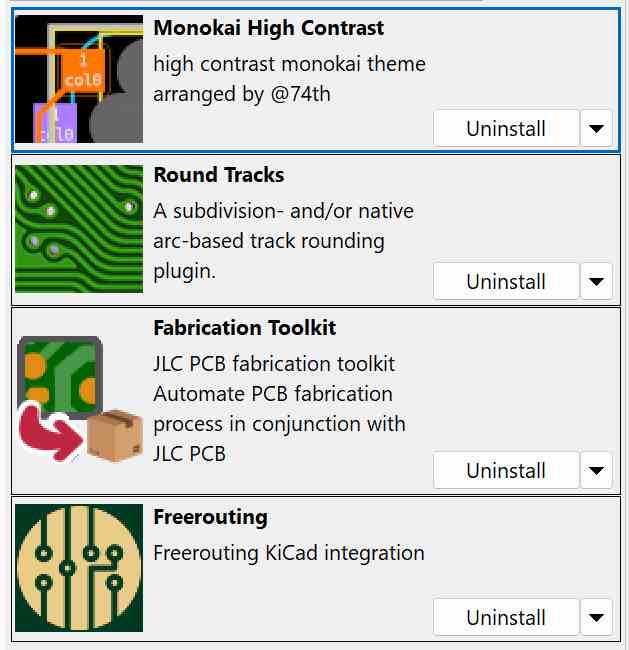 Before starting on the design, I wanted to get some of the plugins I used in the past, as they got uninstalled when I installed Kicad 9. The main plugin that I find very helpful is freerouter, which is an autorouter for Kicad. freerouter isn't perfect, but it is very good for just seeing how your final board will end up looking like. I also have a round track plugin, that I use solely because sometimes it looks cooler than unrounded tracks. I also use a custom theme that works better with OLED screens to save battery, and a fabrication output plugin to easily get all the files required for professionally making my board with JLCPCB. However, atleast on my laptop, all of the plugins did not work for Kicad 9. I found that the schematic editor worked fine with the custom theme, but trying to load the PCB would crash my Kicad. To fix this, I tried uninstalling all plugins 1 by 1 until it worked, but found that non of the plugins worked with Kicad 9
After trying and reverting from the plugins, I ran into one more issue that I assume is plugin related, which is just that one plugin turned off all of my views, so that I could only see what needed to be connected (ratsnest). I fixed this by going to the object settings on the right, and turning back on all of the view icons.
PCB design
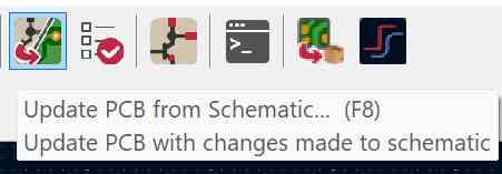 After fixing those issues, I went back to designing the PCB. This is probably the funnest part of making something, as there are no right answers, and it can be made in infinite ways to suit infinitely different needs. As I described above, I wanted it to be millable. This means that one of the strongest tools of PCB design, vias, were not usable, as those are much too small to mill. I also wanted the ports to be easy to access, which is why my final design ended up having the 2 hx711s and their components separated, so that accessing the pinouts on them would be easier.
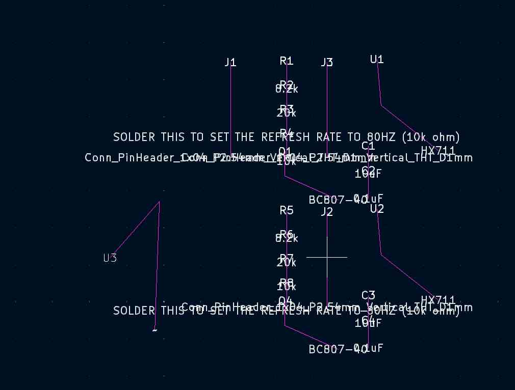
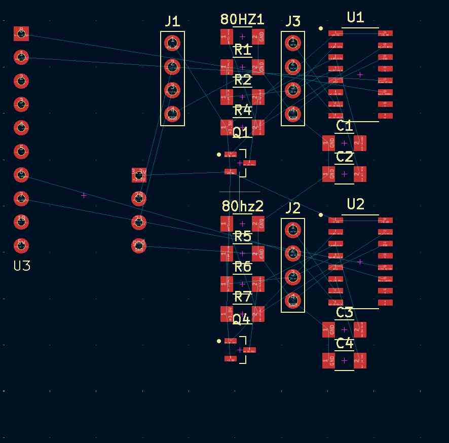
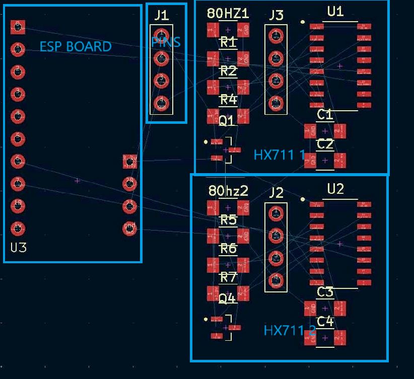
After running the update PCB from schematic tool, I got no errors thanks to clearly defining them in the schematic portion. As seen below, there are 3/4 parts of the schematic, being the esp main board, the first hx711 and required components, the second hx711 and required components, and some pins broken out from the esp32
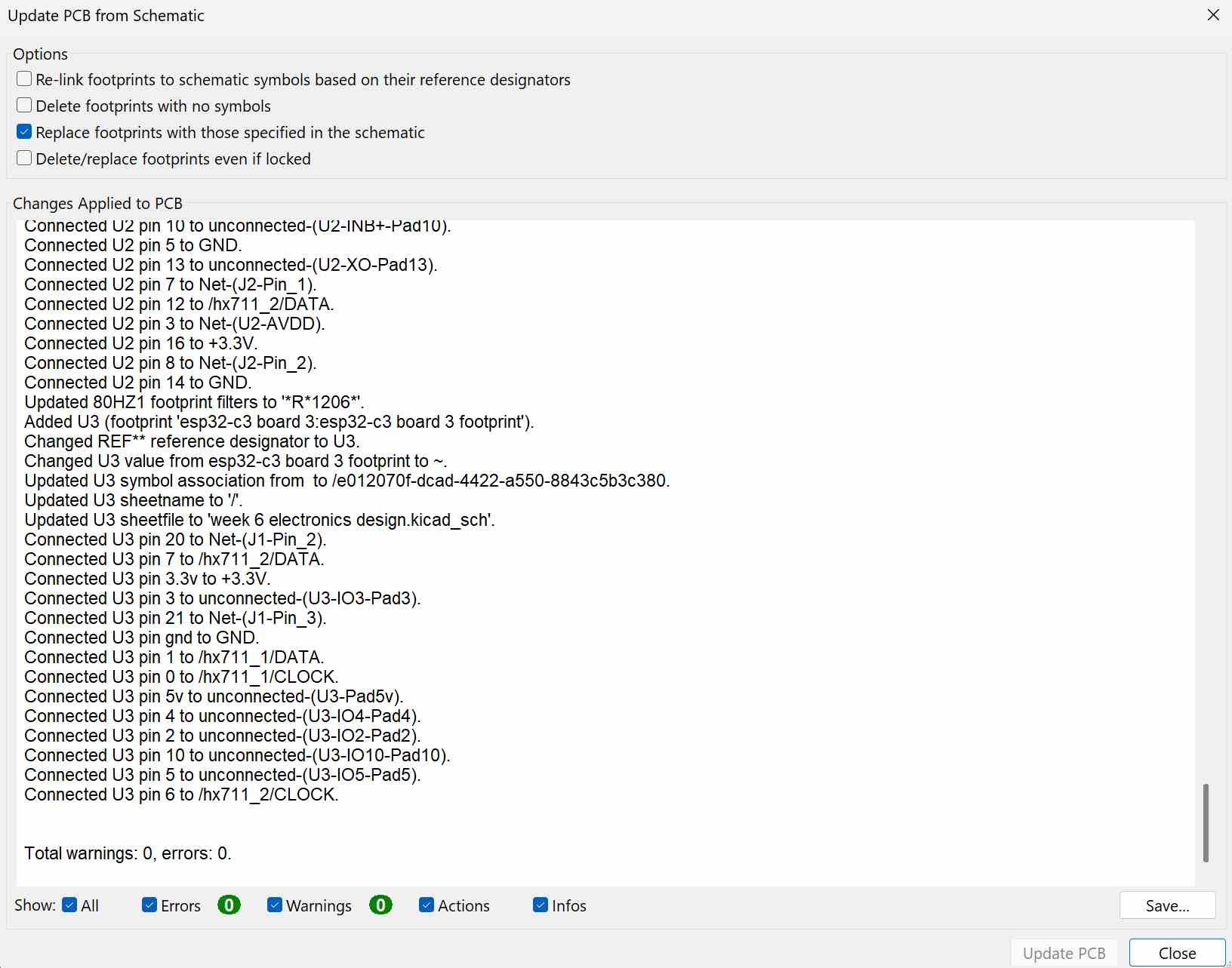
Important Change
before starting to route anything, I made sure to set my trace widths higher than normal. For this, I used .325 as it was just the right thickness to fit between the pads of the esp32-c3 and still getting through the design rules checker without fail
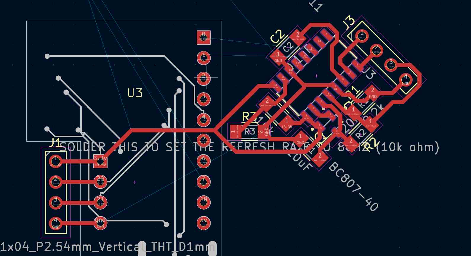
On my first design, I tried compacting the hx711 and its components as close as possible together. However, in doing this I realized that it would be impossible for every component to get where it needed without either vias or a more spaced out approach, leading to it being scrapped after getting to the image below
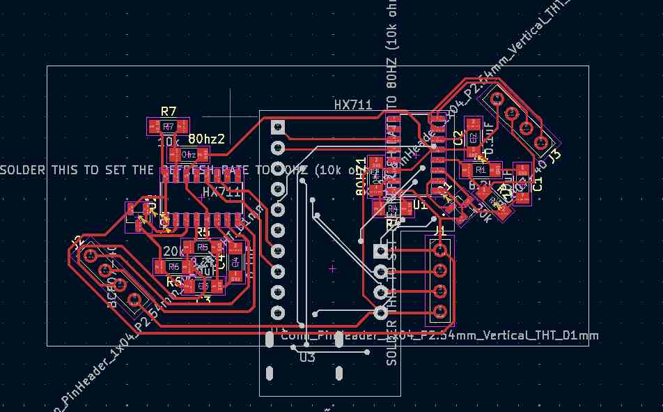
On my second go at it, I faired much better. keeping in mind some of the harder connections, like the two data and clock pins from the hx711, I was able to design first the right hx711 board and breakout, then the right one, which resulted in the image below
For the image here, I just used a basic rectangle for the boards outline (the white line). I did design with a different outline in mind, which is why some components are rotated 45 degrees. Because of the rotation, I was able to make the breakout pins much closer to the edge of the board, which will allow for an easy time working with it
 {}
{}
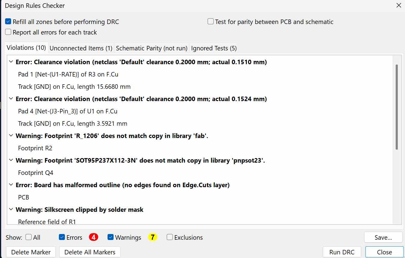
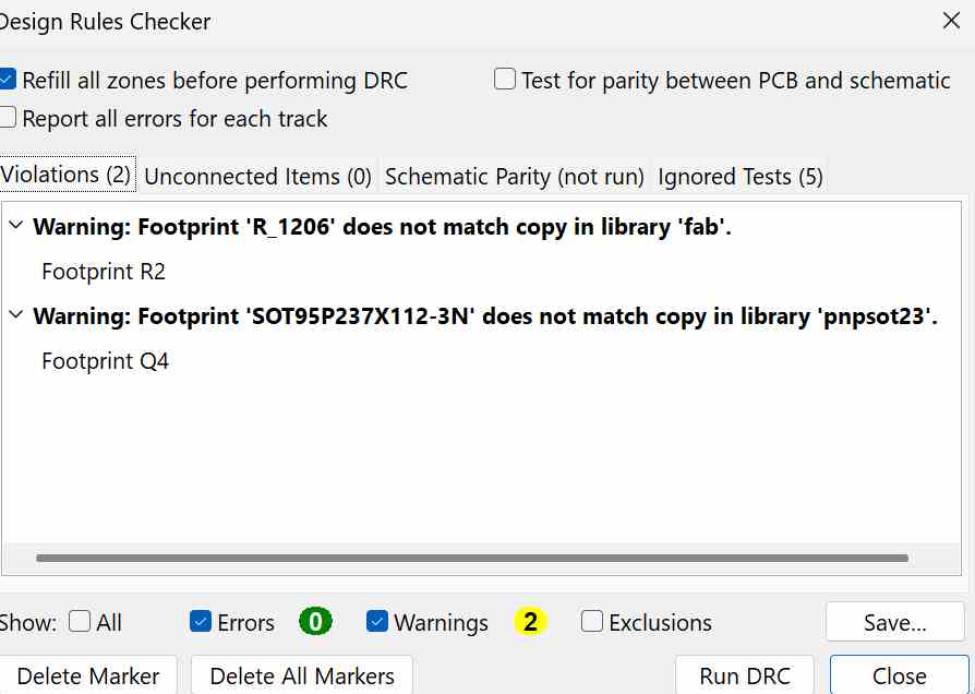
After finishing the rough board, I needed to fix some things. Specifically, after running the Design rules checker, I found where some traces were too close to eachother. By moving those tracks away from eachother, preventing the silkscreen from clipping, and fixing really small holes in the outline, I removed all major problems with the Board. I still have 2 warnings about some components footpritns not matching, but just physically looking at them im able to tell they are the right one, so I im not really worrying about those
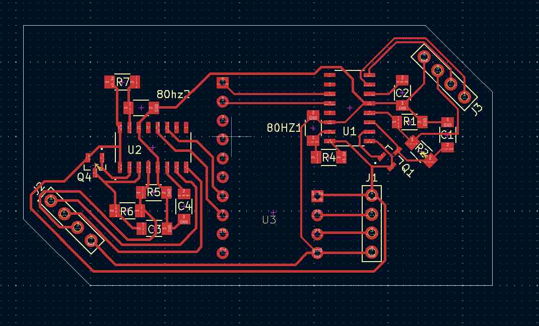
Final Board Design/Hero Shot
There is some wasted space on the top left and bottom right, but I just liked how the board looked as it was so forget about it. I also tried to make the 2 resistors that control the reading rate of the hx711 easy to solder, which means that the one on the left is the topmost, and the one on the right is the leftmost. Just for testings sake, even though I didn't plan to, I put this into bantam tools and got a final time of 9 minutes for the traces alone using a v cut pcb milling bit
Ordering Board Online
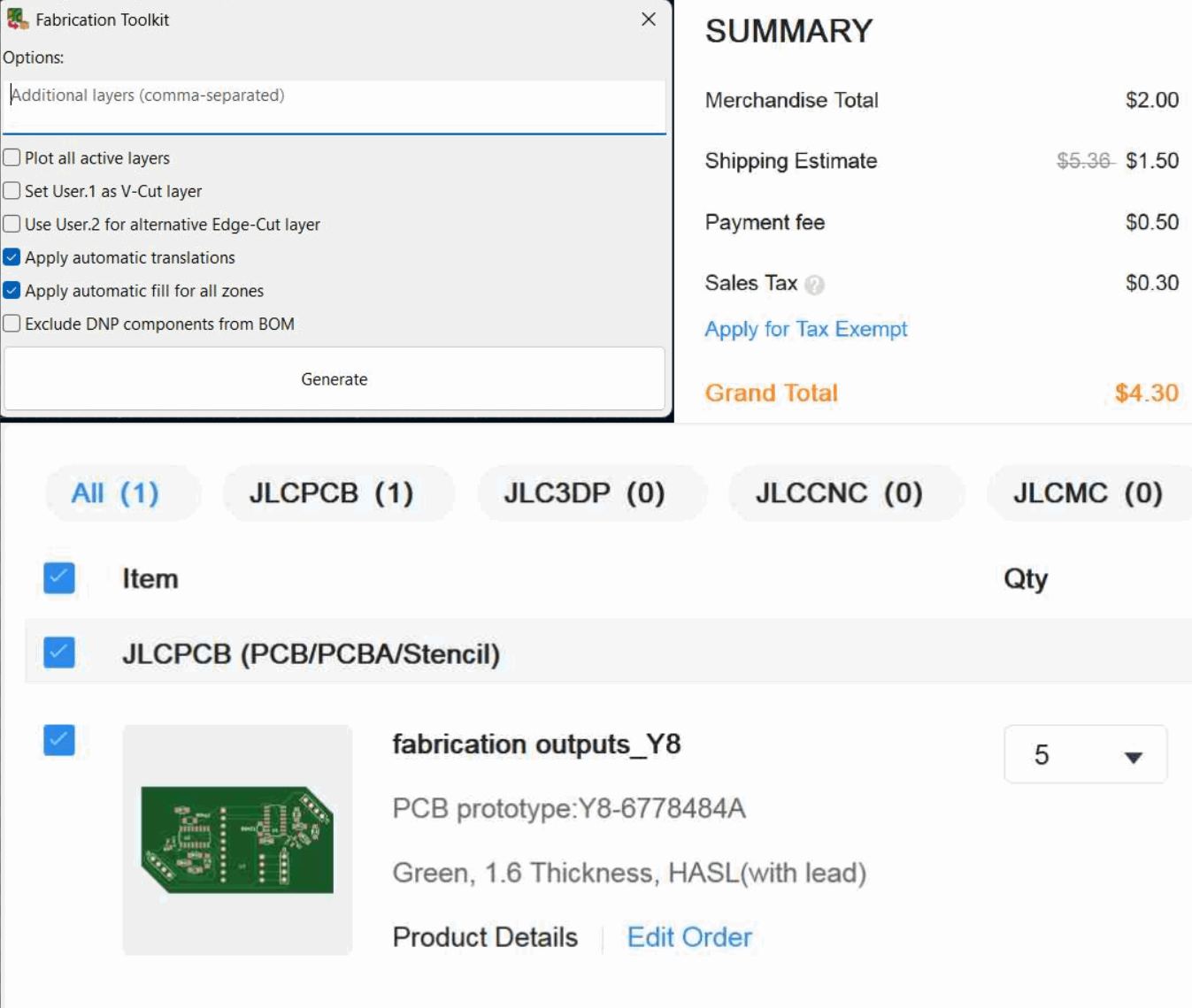
I am not a fan of milling PCBs, they just always go wrong when im involved. Because of that, and the fact that this board might need to survive a fall of over 20 cm, I wanted it made professionally. For that, I use JLCPCB. They are the best in terms of cost only, but they are Very Cheap. For ordering my board, I installed the plugins that didnt work on my laptop onto my computer, where they did work for some reason, and used the fabrication outputs from there to make a file that's template was pre-made for ordering online from JLCPCB After generating the files, I simply uploaded the zip to JLCPCB. I dont change any settings on my order, as JLCPCB always has sales for making 5 pcb's, where it is only 2 dollars when settings aren't touched. For shipping, I used the Global standard direct line, which is the cheapest by far shipping option available, but also takes between 8 and 13 business days to get to me. Im fine with waiting for this board, so I went to it. My final total for getting 5 of these boards professionally made was under 5 dollars, and it would take anywhere between 10 and 15 business days to get to me because of the 2 day build time
Group work
A link to my group work is here
Along with Elle Hahn, our group work for this week was to test the behavior of a microcontroller with "test equipment," which we took as a multimeter, oscilloscope, and logic analyzer. After testing everything together, I wrote about the multimeter and oscilloscope, while she wrote about the logic analyzer. Attached below is a copy of my writing
Multimeter
What is it?
A multimeter is the most basic but useful tool for testing circuits. As seen on ours, it supports reading voltage, amperage, resistance, among other useful tools like continuity (could power flow through this) and testing diodes (which way does the power flow through this).
How to set it up
In our lab, and probably for you, it is already pre set up. The only thing you need to do to get it ready is to switch its dial to what your reading, with the only obscure parts of it being the greek symbol omega being resistance in ohms, and the sound wave/wifi symbol looking thing usually being continuity
How to use it?
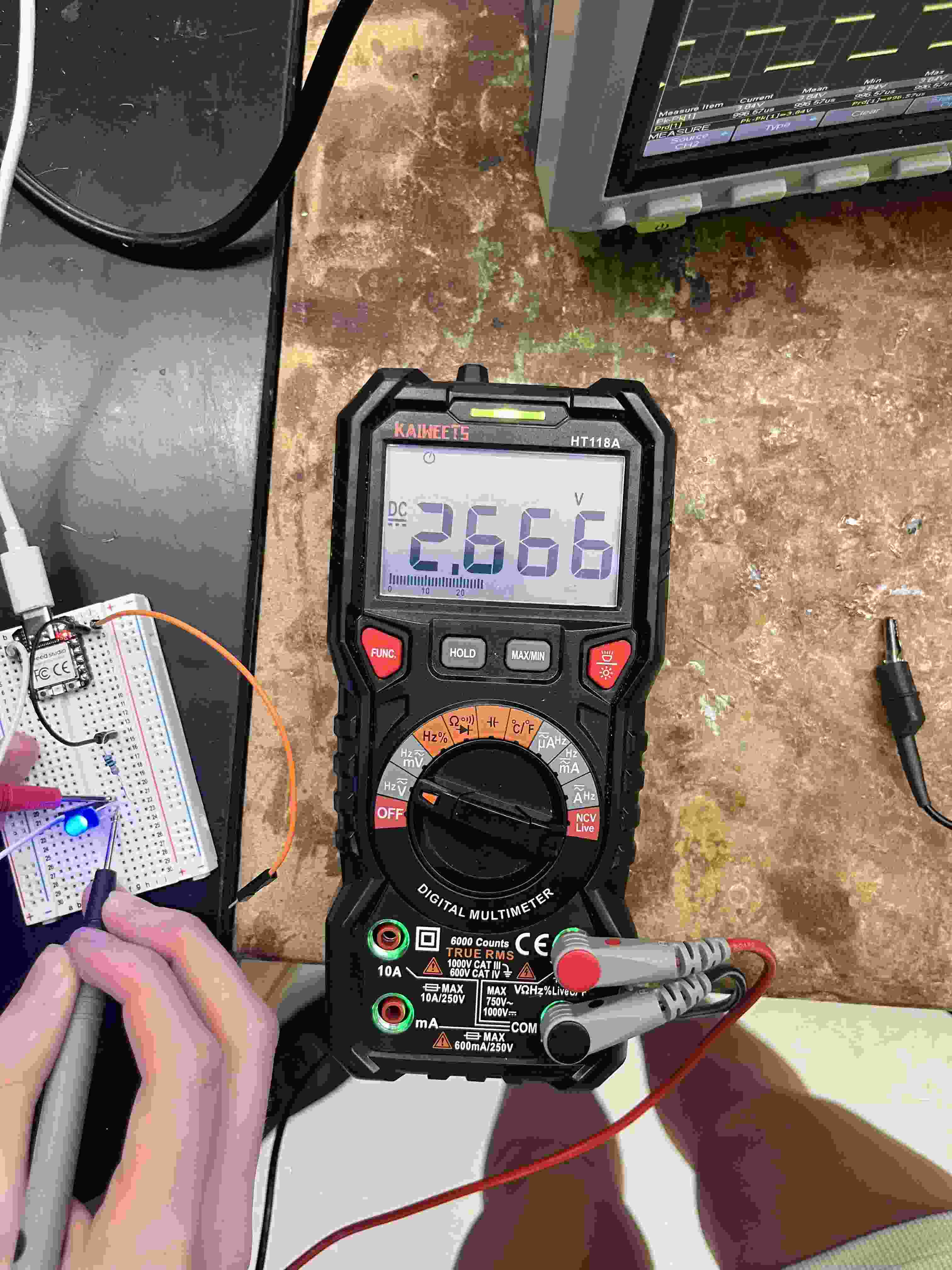
Multimeters are also very simple to use, just requiring the ground probe (usually black) to be connected to ground somewhere and the red probe connected to where you want to see voltage. For resistance, you just measure on the two sides of the resistor, and for current, you break the circuit and let the power flow through. By testing the voltage of an LED being dimmed and brightened by PWM, we were able to see crudely how the voltage was decreasing and increasing. for a deeper understanding, a multimeter is not good, and a oscilloscope or logic analyzer is required.
Oscilloscope
What is it?
The oscilloscope is next to a logic analyzer as the strongest tool for understanding a circuit in our lab. Unlike a multimeter, which only gives static readings, an oscilloscope allows us to visualize how signals change over time. It displays voltage as the vertical component, and time as the horizontal, making it invaluable for analyzing, debugging, and measuring precise timing characteristics in a circuit. Using an oscilloscope, we could observe the shape, frequency, and amplitude of signals. This is especially useful for understanding PWM signals, clock pulses, and simple communication protocols like SPI or I2C.
How to set it up?
Setting up the oscilloscope is complicated on the first run. The main things we had to do were find the wires/probe for it, which was stored in an entirely different room. After that, Andrew Puky, who had worked with the oscilloscope a day before helped guide us through setting it up. Essentially, we had to plug the probe into channel one, select channel one, and then change the window size intil our graph fit neatly in there
How to use it?
By Connecting to ground with the clamp, and the the output of a PWM-controlled LED with the probe, we were able to see the actual waveform instead of just a fluctuating voltage value, showing clearly how the signal switches between high and low states. Oscilloscopes have multiple settings for adjusting the time scale, voltage range, and triggering, allowing us to capture specific moments in a signal. They can also measure properties like duty cycle, rise time, and signal noise, making them essential for diagnosing circuit issues past some part of it not having power.
Reflection
I don’t know if there’s a job dedicated solely to PCB design, but so far, it’s been the most fun I’ve had in my Fab Lab. This week was an opportunity to apply my PCB design knowledge while also confronting my dislike of milling PCBs. With the constraint of making it single-sided, this was my first board that wasn’t just a simple LED and button circuit designed for in-house production.
Even though I didn’t end up milling it, it’s always nice to have an alternative to ordering boards, which can cost $5 and take 14 days to arrive. In KiCad, this was also my first real use of hierarchical sheets. I had used them before in my ESP32-C3 board design, but only for the USB-C port and the two resistors needed for orientation and port type detection. Using hierarchical sheets helped me (1) keep my design cleaner and (2) fix errors more easily with just one edit.
This project also served as a refresher since the last time I used KiCad was over four months ago for my ESP board. Additionally, creating the symbol and footprint for that board was a valuable learning experience that I know will come in handy later.
I’m a bit disappointed that I couldn’t use the plugins I normally rely on. Freerouting, the auto-router, for example, would have saved me hours of trial and error, but since it tends to use vias—and also just wouldn’t work on my system—I had to route everything manually. The design still isn’t perfect. My ESP32-C3 board, for example, has some really awkward vias that don’t serve much purpose and just make the schematic more cluttered.
The group work also helped a lot, as I have never used a oscilloscope or logic analyzer before. I think a logic analyzer will be supremely useful as a last resort, because although how strong it is, it isn't possible to set it up on my laptop due to it being windows on arm, and the fact that my lab, not me personally, owns the logic analyzers.
Overall, electronics design, is a really useful skill to know that I improved on over this week.
Design Files
My Design files are located here, which includes the boards kicad project files, the production output for JLCPCB, and all of my really specific footprint and symbol libraries that I used in this, if you want the files for the esp32-c3 board, go to this page on my site, where it is located at the bottom
Image quality fix
Since week 1 of my fab documentation, I have been using greenshot to take photos, as it automatically compresses them. However, starting this week I noticed that some of my images look absolutely horrible, which caused me to realize that on my laptop, the quality of photos was set to 30/100, which made them look greatly worse. Thats been fixed now, which means that after this week all images should look much better.
