Week 4: Electronics Production
This week’s focus was on the creation of programmable PCB boards through milling, soldering, and coding. All files can be found here.
Requirements:
Group Assignment:
- Characterize the design rules for your in-house PCB production process
- Send a PCB out to a board house
Individual Assignment:
- Make and test a microcontroller development board
- Extra credit: personalize the board
- Extra credit: make it with another process
References:
PCB Board Creation
In the first part of this week, we are instructed to create a PCB board for electronics production. To do this, our lab uses the Bantam Milling Software and the OtherMill Pro milling machine. To do this process, I followed the workflow. I also followed the ideas laid out in the QuenTorres’s documentation for the programming and creation of the board.
Below are the major steps that I followed to create my electronic board.
1) Install Bantam Tools Milling Machine Software here.
2) Bit Installation:
-
Within the jog menu of the Bantam software, select
install tool. -
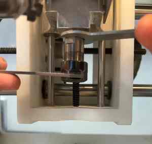
Use proper wrenches to either unscrew a previous bit or loosen the collet.
-
Insert new bit (will be 1/64” for the first pass) and tighten.
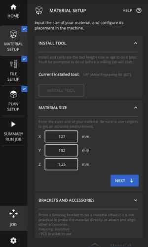
3) Material setup:
-
Select the proper bit in the Material Setup Menu.
-
Select Next or a similar progression button until the bit moves over the base plate, then click
Start. -
After the bit has been probed, configure material size by measuring, for our copper plates the dimensions were 127mm x 102mm.
-
Add double-sided transfer tape to the bottom of the copper plate, making sure that there is no overlap
-
Select
Material Offset Probing Routines. -
Choose
Z-only Stock Probingand make sure that the bit is moved over the material and the clip is on the copper plate, then select the proper progression button. This should give you the information for the depth/height of the material.
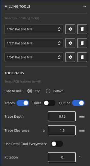
4) File Setup:
-
Import the file.
-
For our file, select 1/64” flat end bit, 1/32” flat end bit, and 1/16” flat end bit
-
Toggle off Holes
-
Set Trace Depth to 0.15 mm
-
Set Trace Clearance to 1.5 mm
-
Set Side to mill to Top
-
Ensure any other details important to your particular milling machine or that have not been mentioned but are a part of the workflow above.
-
Select
Generate GCode Now- a general idea of what the milled product should be will appear.
5) Plan Setup:
- Change the Plan Offset according to material location or other limitations.
6) Job:
-
In the Summary and Run Job menu, select
Mill Single File. -
Click
Okon the menu that appears, and the job will start. -
When prompted to change the bit, do so with the previous instructions
-
Go back into the Re-probe the system with the bit on both the base plate and the copper plate
-
Continue the job and replace the bit again when prompted.
-
When first board is done, use the Plan Setup to move where the cut will be and update the GCode in File Setup
-
Repeat the job process for each board on the copper plate, then remove from base plate.
Throughout this process, I worked with Angelina Yang, Alana Duffy, and Ryan Zhou at the same milling machine. We first downloaded the .brd file given to us by our instructors, which can be found in the download above.

Milling schematic in Eagle, a workspace/program which is part of Fusion360

Circuit schematic in the QuenTorres documentation
We were initially blocked from using the software due to it constantly reading “Initializing” on the bottom of the screen and preventing any actions from being taken. After restarting the computer, the error disapeared and we started setting up the file.
After the file was imported, we selected the correct settings in File Setup that are included the steps mentioned in the workflow above.
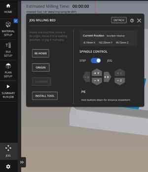
Go Jog > Install Tool to move the spindle to the front and center of the machine so that we could change the bit.
With the two wrenches, the smaller one was inserted onto the top slot of the spindle and the larger one was placed around the collet on the bottom of the spindle.
A 1/64” bit was pushed into the spindle and was tightened. In Material Setup > Install Tool, 1/64” flat end mill was selected and we clicked “Next”. The spindle should move over the base plate, at which point we confirmed to make the bit move down until it touched the base plate. The bit slowly moved down until it touched the base plate, then moved back up. This calibrates the depth of the bit, which helps ensure that the bit doesn’t go into the base plate.
The next step was to insert the copper plate, which was done by first acquiring and measuring the copper plates given to us by our instructors. We measured them to be 127mm x 102mm, and put this into the Material Setup > Material Size.
We applied doubled sided Nitto tape to the bottom of the copper plate, making sure that there was no overlap.
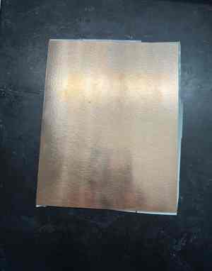

The bottom and top of the copper plate.
We aligned the copper plate to the bed of the milling machine and placed it in, with the nitto tape serving to keep it all together.

We probed the bit (i.e. checked the height of the copper) with Material Setup > Material Offset Probe Routines, selected “Z-only Stock Probing”, and used the Jog menu to move the bit above the copper. Select “Start” to have the bit move down and probe.
Video of the machine probing the bit.
This set the depth in Material Size to the difference between the height of the copper and height of the base plate, which was 1.79mm
Now that all the proper settings are configured, I generated the g-code in File Setup. This created a visual of what the milling machine would cut out from the copper plate. There were red lines initially, meaning that the bits were too small to cut out some of the lines, but this was due to the 1/16” bit being unselected. It was reselected and the red lines disappeared.

In the Plan Setup menu, I changed the Plan offset slightly because it appeared as if the gcode was intersecting with the border of the copper. I had to update the g-code again after this because, even though the display appeared to update, the g-code had not.
The final step was to go do Summary & Run Job > Mill Single File. This started the whole system and begins milling. The system prompted me to change the bit twice thorughout the process of the milling to the 1/32” and 1/16” flat end bits for different sections of the milling job, which I did without complication.
Video of the first milling job.
Now that the first piece had been milled, I had to vacuum off the surface before we could begin to mill the other pieces, so the lab’s vacuum was used to clean off all the metal particles.
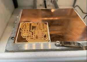
The first piece after milling and cleaning.
This process had to be repeated three other times for the other people that I was working with, meaning that we had to rerun the job three time with different offsets in the Plan Setup menu. Those offsets are the following:
-
x = 4 mm, y = 3 mm
-
x = 70 mm, y = 3 mm
-
x = 70 mm, y = 54 mm
-
x = 4 mm, y = 54 mm
The milling of the last piece.
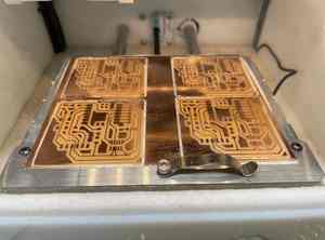
The four PCB boards after being milled and vacuumed.
With the four boards having been completed, they were cleaned off and each of the people that I was working with recieved their own.

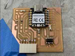
An individual PCB board.
Soldering
With the first part of the creation of the board done, I moved onto soldering.
Compenents:
| Compenents | Quantity |
|---|---|
| Xiao RP2040 | 1 |
| Blue LEDs | 3 |
| Conn header SMD R/A 6POS 2.54mm | 1 |
| Conn header SMD 10POS 1.27mm | 1 |
| Tactile Switch | 1 |
| 1K Ohm 1206 Resistor | 4 |
| 490 Ohm 1206 Resistor | 1 |
| Milled PCB board | 1 |
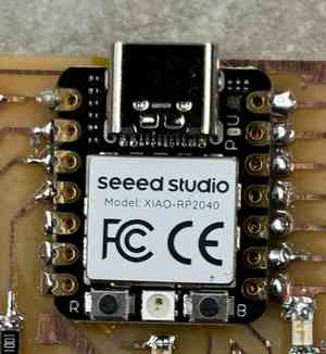
To start, I placed insulating kapton tape on the back of my Xiao RP2040 to make sure that it wouldn’t short circuit from the traces of the board that were underneath it.

Now I began to solder, but since I had already had significiant experience with normal soldering, I wanted to try something else. Based off my instructor’s suggestion, I used lead-free solder paste to do all the soldering for the PCB board. To use it, the paste is pushed out of the syringe and onto the connection area, and, when heated, the paste easily melts and forms the connections. I prefered this method over the preivous ways I was soldering, especially due to how solder bridges were much tougher to create on the spaced out traces of the board. After applying tape to the board to keep it from moving, I soldered on the RP2040.
The following component was the LEDs. Working with Angelina Yang, we checked the schematic for the design to determine the direction they had to face in order to deal with the polarity of the pieces. I also used a multimeter’s diode feature to see what the green bit on the side of the piece meant, and this also helped us know more about the polarity of the component.

I soldered on the header pins next, but something obvious I noticed was that the 1.27mm header pin component that they gave us was far too large to fit, so I grabbed the new piece from our instructors. With this new piece, I also experienced minor difficulties with solder bridges, but examining other student’s boards showed that this was an intentional part of the traces that I had forgotten about and the two spots were supposed to be connected.
I soldered on the tactile switch after. I saw a small metal bit on one side of the button and discovered that this indicated how the component needed to be oriented. For this board, the bit had to be up or down.

The final step was to solder on the four 1K Ohm resistors and one 490 Ohm resistor.

Since this was the final thing I had to solder on, I could now begin working on the code.
Coding/Programming
I started by downloading ArduinoIDE here and used it as a guide on how to program the board. The first issue I encountered was an installation error that repeatedly happened. From the QuenTorres guide, I copied a link that I had to put in to the “Additional Boards Manager” section of the ArduinoIDE preferences, but this link kept disappearing whenever I exited the preferences menu. I ended up doing most of my work on the school computers, but this issue was fixed later by switching to a newer version of the software.
In the software, I wrote a simple blink code to make each LED turn on and off at different intervals that I chose.
void setup() {
  pinMode(26, OUTPUT); // initializes the pin for the top left LED
  pinMode(1, OUTPUT); // initializes the pin for the for the right LED
  pinMode(0, OUTPUT); // initializes the pin for the for the middle LED
}

void loop() {
  digitalWrite(26, HIGH);
  digitalWrite(1, HIGH);
  digitalWrite(0, HIGH);
  delay(500);
  // turns on the LEDs

  digitalWrite(26, LOW);
  digitalWrite(1, LOW);
  digitalWrite(0, LOW);
  delay(1000);
  // turns off the LEDs
}
When plugged the chip into the computer and ran this code for the first time, nothing happened. I used the diode feature of the multimeter to check each LED, and I found that the top left one did not turn on when connected to the multimeter. I examined the LED and saw that it appeared to be burnt out, so I went to replace it by soldering on a new one.
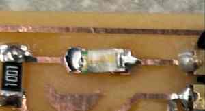
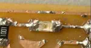
Comparison of the bad LED (left) and new LED (right).
I plugged the RP2040 back in and ran the code and saw that it successfully worked. However, just before I was about to take a video, one of my fellow students walked up and simply tapped the board, which made all the LEDs shut off. In my confusion, I mentioned what had just happened to my instructors, and they told me that there may be an issue with my soldering and the programming chip had been detatched from the PCB board. I used solder paste again to add more to both sides of the RP2040, hopefully strengthening the connection and preventing it from disconnecting again.

Before (left) and after (right) of adding more solder.
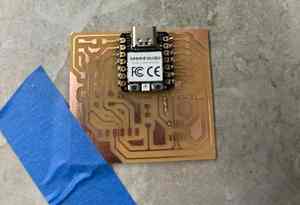
Now that all the issues were solved, the board worked.
The blinking LEDs connected to the RP2040.
The next step was to program the switch on the board. From this RP2040 guide, I learned how to implement the code necessary to make the LEDs only turn on when the switch was pressed.
int buttonState = 0; // defines the buttonstate variable to 0 or off

void setup() {
  pinMode(27, INPUT); // initializes the pin for the button as an input
  pinMode(26, OUTPUT); // initializes the pin for the top left LED
  pinMode(1, OUTPUT); // initializes the pin for the for the right LED
  pinMode(0, OUTPUT); // initializes the pin for the for the middle LED
}

void loop() {
  buttonState = digitalRead(27); // sets the input from the button to either High or Low
  if (buttonState == HIGH) { // checks if the button state is HIGH/on/pressed
    digitalWrite(26, HIGH);
    digitalWrite(1, HIGH);
    digitalWrite(0, HIGH);
    // LEDs are turned on
  } else {
    digitalWrite(26, LOW);
    digitalWrite(1, LOW);
    digitalWrite(0, LOW);
    // LEDs are kept off when the button is not being pressed
  }

}
The switch controlling the LEDs.
Group Assignment
Our group project for this week involved characterizing the design rules for the in-house PCB production process of the Bantam software that we use. This involved figuring out the document feed, speed, plunge rate, tools, and depth of cutting. You can find our documentation here.
Individual Contribution
I assisted in researching and defining the terms presented in the table at the beginning of the document, and I also helped mill the line test by switching some of the bits and helping configure the file in the Bantam software.
Reflection
The week granted a significant level of insight into the milling process, and, moreover, how to create a board that can be programmed. I believe that this week will definitely prove highly useful in the future when more boards are needed for other projects in the future. This seems a vital step in the process of learning how not just to manufacture a design, but also make it do tasks that you designate it to do.
The troubleshooting and the long hours involved with this week (staying in the school lab until 11:30 PM) are both unfortunate indicators of what is to come in the future and beneficial to the process of learning how to correct errors instead of always staying on a provided path. Additionally, these errors also allowed for a more in-depth understanding of how the boards worked, mainly with the importance of connections and wiring.
Though tough, this week was enjoyable, and being able to actually create the whole board instead of using the previous, simpler methods involved with the school’s courses felt rewarding.