Week 8: Electronics Design
This week’s goal is to design a board for a microcontroller and other components in order to program the board. This involved trying out different EDA tools, KiCad and Eagle, to see which one I prefer. After designing the board in one of these softwares, it has to be milled, soldered, and successfully programmed. Files can be found here.
Requirements
Group Assignment:
-
Use the test equipment in your lab to observe the operation a microcontroller circuit board.
-
Send a PCB out to a board house.
Individual assignment:
-
Use an EDA tool to design a development board to interactand communicate with an embedded microcontroller, produce it, and test it.
-
Extra credit: Try another design workflow.
-
Extra credit: Design a case for it.
-
Extra credit: Simulate its operation.
KiCad
KiCad is a free software for electronic design, manufacturing, and automation. Its primary features include a schematic editor that allows one to place components and make connections, a symbol editor which allows for the creation of new symbols for the schematic editor, a PCB editor where actual connections are created based on both footprints, which are real representations of symbols, and the requirements of the board.
I followed this official tutorial from KiCad’s website to make my first design in KiCad. The first part of the tutorial explained how to set up the schematic, pcb, and overall project files. The second part explained the setup of the schematic tab and how to create connections and power/ground symbols. This section also explained assigning values and footprints, which are a critical part in the manufacturing and PCB side of things. The third part of the tutorial detailed how to use the PCB editor to route the connections between the components, and how to properly set up the board space for design. It also showed off the 3D viewer option of the PCB editor, which shows all the connections and components with 3D models on a sample PCB. The final part of the tutorial discussed how to create custom symbols and footprints, for this is an important step in designing a board when a singule specific piece may not already be in a downloaded library. I found that, while a bit too simple and lacking in complexity, it did help establish a good foundational understanding of how to use KiCad. Below are images from different steps of this tutorial alongside short descriptions of each.

The schematic during the initial designing.

The PCB designer during the intial designing.

The custom symbol (left) and footprint (right) for a new component.
The schematic and pcb editor after this component was incorporated in.


The top (right) and bottom (left) of the 3D viewer at the end of the tutorial.
While this tutorial did have worth in teaching the very basic fundamentals for KiCad 8.0, I still found it a bit difficult to follow and sometimes struggled to know where to navigate to to find a specific operation, function, or tool. I did like the visual simplicity and the camera controls (which are a pretty big factor for myself), so I ended up prefering it over the next EDA software.
Eagle
Eagle is another EDA software which is now built into Autodesk Fusion360, and because of the educational license gratned by our lab, I was able to easily use it. I followed a playlist of tutorials that were taught by George Garcia, a community manager for Fusion360, and to help myself follow these videos, I used Adam Stone’s documentation for help on understanding. The first video was directed towards simply setting up the project in Fusion360, and to do this, you simply go to File > New Electronics Design. This creates a schematic file, a pcb file, and a overall viewer file that shows both of the former at once. Through the files that this creates, one can begin to create almost anything that they need to, provided that required libraries are installed onto the user’s system or the files they need are already part of the pre-installed set.
The second video starts out by showing off a library that would be important for this tutorial, but he did not explain where to find it. Thanks to Adam, I went to this website, downloaded the library, uploaded it into the folder I was using for this project, and continued on with the tutorial.
After this section, I began to follow his instruction to draw nets between imported components and add labels to different sections of the electronics, leading to my final schematic file looking like this:
The next step, before actually modifying the pcb file to significant degree, was to create a pcb outline and 3D file to accompany the electronic design. This step isn’t required for every single design in Eagle if the software is just being used to create the manufacturing files themselves, but creating a corresponding board helps visualize how it can be incorporated into a larger project.
First, I partially recreated the 3D file that he showed off rather than importing it like I did for the library.
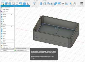
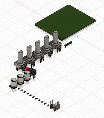
As can be somewhat seen, the sketch in the box is slightly raised up and split into two halves. There are multiple ways to be able to create outline for the pcb file from here, mainly the independent and associative methods. The independent creates a “snapshot” of the current profile it is based on and uses that as the outline for the pcb board, while the associative can be changed if the profile is also changed. I decided to use associative, even though it didn’t matter too much for the purposes of this tutorial. Then, I linked the unaltered pcb file to this board, leading to a bunch of scattered components appearing off the board.
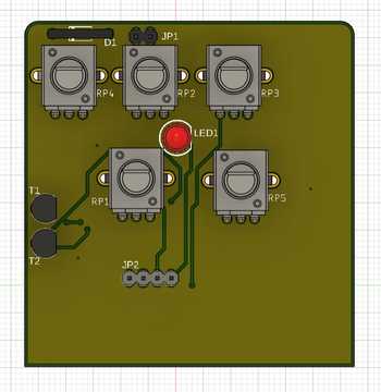
The next and final tutorial detialed how to link up all the components and put them in the correct places and on the correct layers. In Eagle, red means the front of the board, blue means the back, and light green represnts holes in the board. After following along, I ended up with a pcb file that looked like this:

Then, I went back to the 3D space and updated the pcb, which changed both the bottom and top of the board.
The top (left) and bottom (right) of the board after being updated with the connections and 3D models from the library earlier.
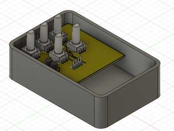
I inserted this file back into the 3D box I made before and moved it up a little so that the components wouldn’t be intersecting with the box.
This ended the Eagle tutorial portion of this week’s assignment, and I could begin to start work on designing my own board. After using Fusion360 for CNC week right before this and the fact that I was also using it to model out my final project, I wanted to get out of the software, so I chose KiCad.
Designing the Board
For the creation of our board, Mr. Dubick outlined a few base requirements/suggestions: a) use an ATtiny412 chip b) include a capacitor for the power to ground c) an LED indicator that is always on when you plug in the board d) a programmable LED e) a button. The rest of the board is meant to connect to other sensors or electronics in later weeks.
The first step that I took was to download the fab KiCad library found here, which provided symbols and footprints for commonly used items in the Fab Lab. Once I had these files, I began to try and design something that I thought would hopefully work to some extent. Since I had done the SAMD11C chip instead of the ATtiny412, I was a bit inexperienced in how to make the connections between the components.
I utilized the connections on Collin Kanofsky’s documentation to try and connect some of my board. It took me a fair bit, but I eventually created a board that did not have any errors in the ERC, besides a naming issue that was only happening because of an visual choice.
I updated the PCB design from this schematic and began to start routing connections, but noticed that there was a strange error going on with one of the resistors in the middle.
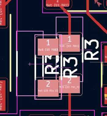
I couldn’t select some random pads and borders that were duplicated off of a resistor, though I could still move the resistor itself. I moved everything away from this error, and saw that the pads of the button were also being affected. I decided to try and revert to a previous save after copying all the normal components, but when I reverted the software did not let me paste what I had copied. However, I had an image on my phone of the schematic that helped me reconstruct it. After doing so, I also added a small amount of text to signify that it was my PCB, though I doubt anyone made a design that looks just like mine.

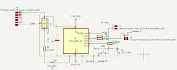
This technically could have worked for this week, but after attending a help session led by Mr. Dubick, I moved different things around, replaced the 1x6 header pins with a three pin version, and replaced both header pins of the two 1x2 header pins with 1x3 so that they could have a PWR pin, a GND pin, and a programmable I/O pin. I changed up the schematic some to be able to alter it this like this, as well as increased the trace/track width to 0.5mm from 0.2mm.
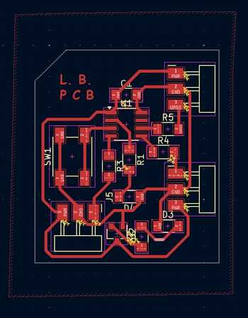
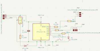
The final designs for both the pcb and the schematic.
I used the 3D viewer to get an additional view of how the board might look upon being milled. Only the ATtiny412 chip had an associated 3D model, so nothing else appears physically on the board.

Since the file had been fully set up, I followed this short tutorial on how to set up the Gerber files for production. I used the plot feature of the pcb editor to put the files into a folder I created, and then I compressed this folder to a zip file and opened it up in the Gerber Viewer of KiCad. I toggled on all the layers and saw a neat file that accurately showed my pcb design.

With everything for this section, I had to hope that the product after milling and soldering would work, since this process took a pretty long time for an inexperienced user.
Producing the Board
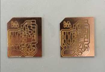
To create the board, I follow the same milling procedures done in previous weeks, which includes importing the proper gerber files into the Bantam Milling software, setting up the file properly, probing the bit, changing the bit during the milling process, and cleaning the area after the board is milled. I decided to mill two boards to have a backup in case something happened to the first, but the second one ended up being worse than the first due to some improperly milled traces in the corner.
Then, I began to get together the correct components, but during the soldering process I was informed that the two resistors which each connected off to different connector header pins were unnecessary, so they were just replaced with 0 Ohm resistors to save having to remill the file. An additional important change that also occured, which is being mentioned now for the sake of a list of components that can be put where it is most relevant, is that the resistor going from the UPDI pin of the connectors pins with the PWR, GND, and UPDI connections did not need to be there, so that was also replaced with a 0 Ohm resistor. I will update the file so that those who wish to download it do not have to deal with that, but I chose not to remill to the board to fix this simple issue. This means that this component list is for my board exclusively, and the 0 Ohm resistors are not needed for future manufacturing.
| Components | Quantity |
|---|---|
| ATtiny412 Chip | 1 |
| 2.54mm Conn. Header Pins 3POS | 3 |
| 0 Ohm resistors | 3 |
| 1uf Capacitor | 1 |
| Tactile Switch | 1 |
| Blue LED | 2 |
| 499 Ohm resistor | 2 |
| 5V Voltage Regulator | 1 |
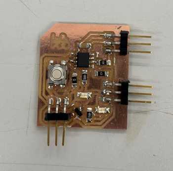
I soldered on all of these components, but I initially had a 4.99k Ohm resistor in place of what became the 0 Ohm resistor for the UPDI pin. This was a bit of a rushed job so I apologize for the less than optimal soldering job.
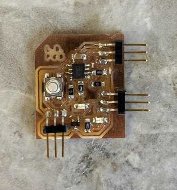
Once this was successfully created, I took an extra UART to UDPI convertor board that Connor Cruz had very graciously created for me, and I soldered on a 6POS 2.54mm male header pin to one side to connect into the QuenTorres board from previous weeks, a 4.99k Ohm resistor, and a 3POS 2.54mm male header pin. Since the pins for my board did not align with the connections for the converter board, I chose a male header pin so that I wouldn’t accidentally connect them together.

Additional details on this board, such as the schematic and file, can be found in my fellow student’s documentation.
Now that all the components had been properly soldered on, I began to start the programming process, which did still end up having some amounts of soldering in it.
Programming
Indicator LED
The first thing I attempted was to plug the UPDI converter into my QuenTorres board and use jumper cables to attach the PWR pins and the GND pins, as I had a LED that is meant to turn on whenever there is power to signify whether or not the board is recieving power properly. When I plugged in the PWR jumper cable, the voltage regulator started smoking! With the help of Collin Kanofsky, I figured out that the orientation for the regulator was wrong, so I looked at the datasheet for the piece to know what to change.
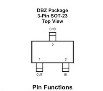

As can be seen by comparing the pinouts to the wiring for my board, the orientation was completely messed up. However, I did not give up on this board since I had already soldered on all the other components, so I got to finagling. I grabbed a new regulator and rotated it, as I knew that the connections would line up if I did so.
Although the soldering job was quite horrendous, it seemed to work for now, so I plugged the wires back in and saw that the indicator LED successfully turned on!

Now, I could get to programming the actual LED through UPDI.
Programmable LED
With my initial attempt to program the board through ArduinoIDE 2.3.1, I chose all the correct settings for an ATtiny412 chip, the correct port, and “SerialUPDI - FAST: 4.5V+ 460800 baud” as the Programmer and then ran the following code:
int pin = 0;

void setup() {
  // initialize digital pin LED_BUILTIN as an output.
  pinMode(pin, OUTPUT);
}

// the loop function runs over and over again forever
void loop() {
  digitalWrite(pin, HIGH);  // turn the LED on (HIGH is the voltage level)
  delay(1000);                      // wait for a second
  digitalWrite(pin, LOW);   // turn the LED off by making the voltage LOW
  delay(1000);                      // wait for a second
}
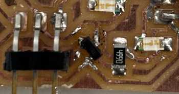
However, I got an error stating that no programmer was found. I tried the same code out in ArduinoIDE 1.18.19, which I also had installed on my computer, and, after selecting all the correct settings once more, I recieved an error which said pymcuprog.pymcuprog_errors.PymcuprogError: UPDI initialisation failed. I was unsure of what this meant, so I pasted the error into google and found this forum discussing how a similar issue might be related to the resistors in the board. This is the point where I went back and replaced the 4.99k Ohm resistor that connected to the UPDI port on the board I created with a 0 Ohm resistor, as the UART to UPDI converter already had a 4.99k Ohm resistor built onto it. This is what the final board looked like after all the corrections were made:
With this having been fixed, I reran the code but got the same error. I was then directed back to ArduinoIDE 2.3.1, where I discovered the “Upload Using Programmer” tool under the Sketch menu. When I ran this, I recieved some good looking text in the output menu.
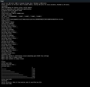
This resulted in the LED beginning to blink!
This was now the end of this week’s work, which was a very exciting fact, as I had effectively gone through most of the embedded programming assignment in just one night (excluding the file creation process).
Group Project
The group project for this week, as told by Mr. Dubick, was to use a multimeter and oscilloscope to measure changes in voltage amounts over time. The documentation can be found here.
Reflection
This week had a very rough start, but once I got some momentum, I was able to make it all the way through. Learning how to use these softwares is an incredibly valuable skill that I am glad to have for future designs, but the time spent on documenting this portion was not fun, especially when I am already low on sleep. The knowledge know of how the connections for a board like this work will be very valuable in the coming weeks, and the outputs will hopefully be made easier. Despite being behind due to spring break, I made it through this week and onto the next one.