Week 6: Electronic design
group project: use the test equipment in your lab to observe the operation of a microcontroller circuit boardindividual project: design a development board to interact and communicate with an embedded microcontroller
extra credit : try another design workflow
extra credit : make a case for it
extra credit : simulate its operation
- For our Lab, the group Assignments can be found:
- The individual assignment for this week happened as follows:
- Installing the software that does the PCB design.
- Choice of the microcontroller unit to interact with.
- Designing the schematic for the circuit.
- Converting the Schematic into the Board.
- Programming the interaction i would have with the MCU.
- Interacting with the circuit in the simulator.
INTRODUCTION TO PCB DESIGN
CIRCUIT GENERATIONS:
FIRST GENERATION - WIRED CONNECTIONS
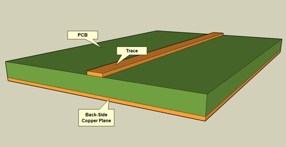
SECOND GENERATION - PRINTED CIRCUIT BOARDS
THIRD GENERATION - IC DESIGNING (VLSI)
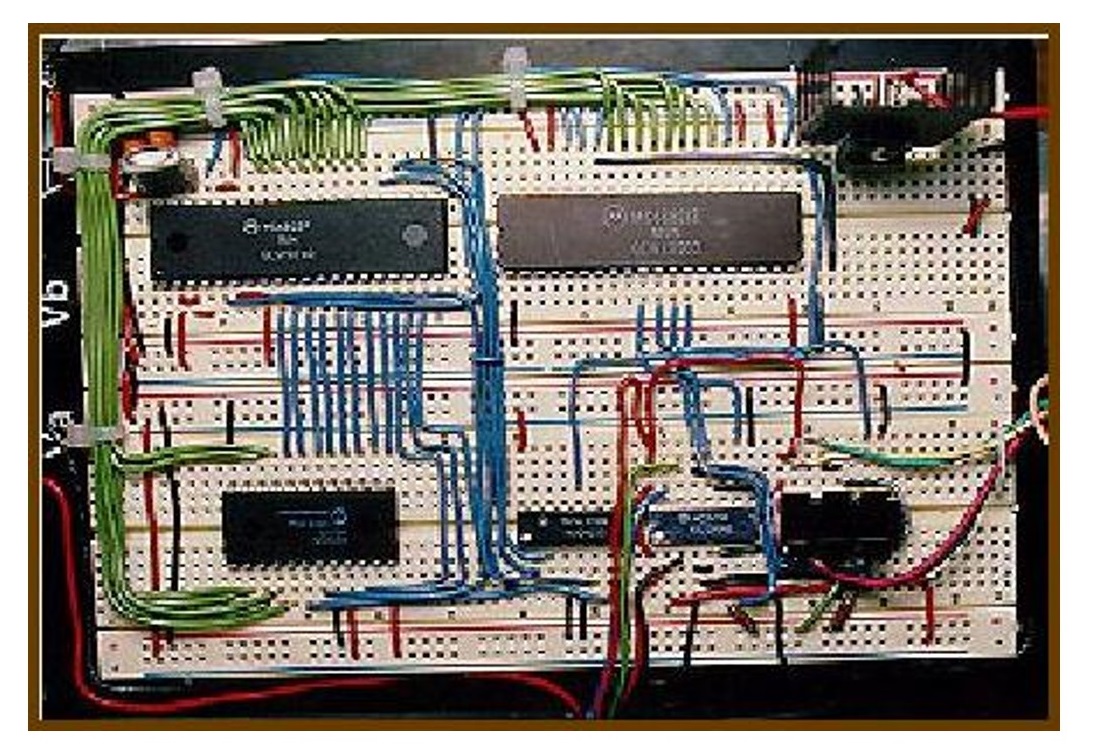
First Generation description:
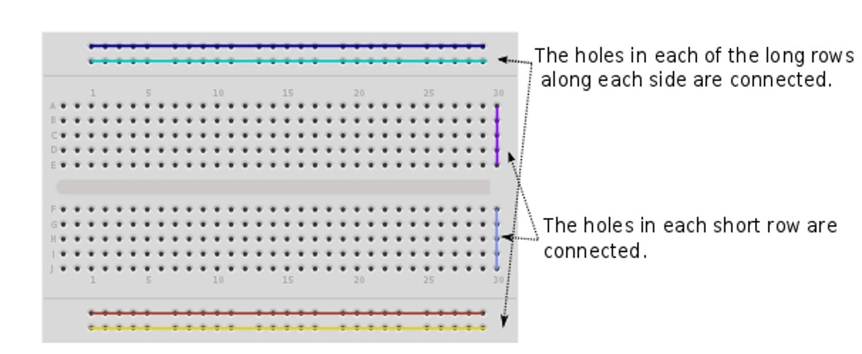
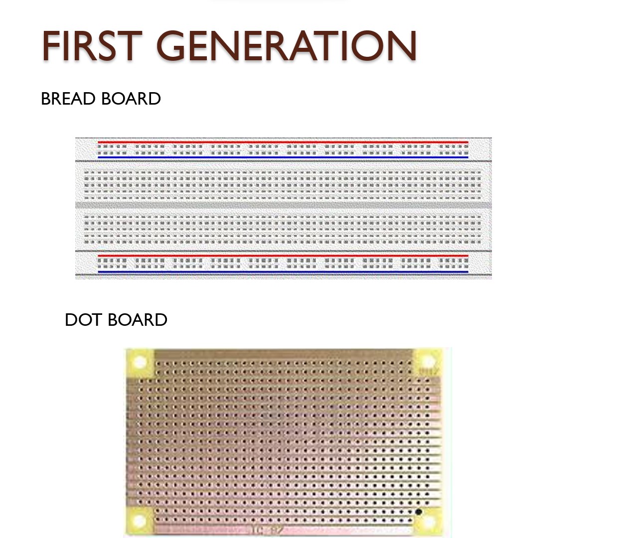 the breadboard's internal orientation and CONNECTIONS:
 However, this carries a limitation in how many components it can host, also wires make a mess. Not to mention that over the time,
connection holes wear out and become loose.
However, this carries a limitation in how many components it can host, also wires make a mess. Not to mention that over the time,
connection holes wear out and become loose.
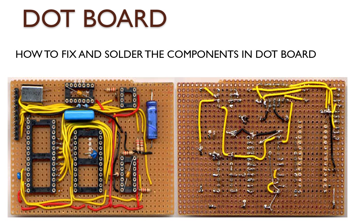
 the Dot matrix was no different in terms of complexion adaptability
 SECOND GENERATION description
PCB: A flat plate or base of insulating material containing a pattern of conducting material (Copper) in it
SECOND GENERATION description
PCB: A flat plate or base of insulating material containing a pattern of conducting material (Copper) in it
 Now a days, we are using different software to design PCB
EAGLE
ORCAD
FREE PCB
EXPRESS PCB
PROTEL
TINA
KiCad
proteus ISIS professional and many more,...
Now a days, we are using different software to design PCB
EAGLE
ORCAD
FREE PCB
EXPRESS PCB
PROTEL
TINA
KiCad
proteus ISIS professional and many more,...
ADVANTAGES:
- many circuits can be etched simultaneously,
- Compact circuit design can be achieved,
- Wire connections are not necessary,
- Easily understandable circuits.
DISADVANTAGES:
- Once designed and etched, we can not change the circuit easily
Have to redesign and to etch the new circuit in different copper board
- Harmful chemicals are used for PCB manufacturing
GLASS EPOXY BOARD (SILK SCREEN BOARD):
Glass epoxy board is fixed back to copper plate.
This board is preferred while design circuits that carry large currents.
 Types of PCB:
SINGLE LAYER PCB: Components are mounted on one side of the board and the conductor pattern on the other side.Suitable for simple circuits only
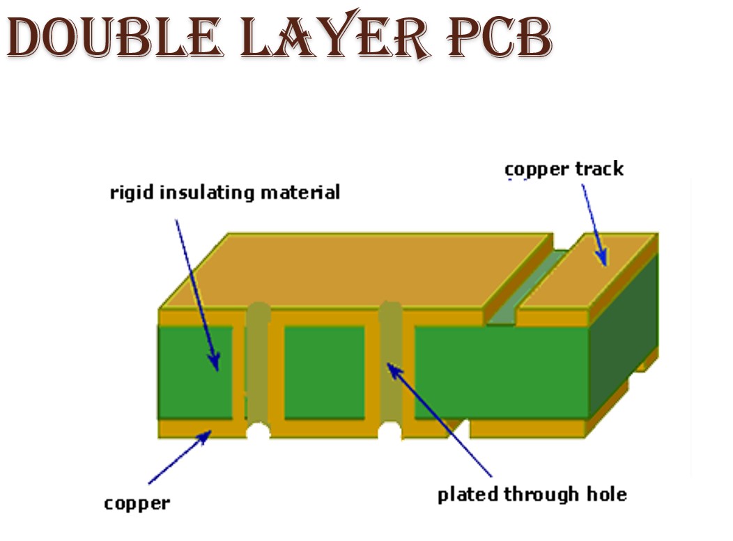
DOUBLE LAYER PCB:They have twice the area for the conductor pattern compared to single-sided PCBs
Having conductor pattern on both sides of the board
Top layer conductor pattern and bottom layer conductor pattern are connected by vias
The vias described in Double-sided PCBs always penetrate the whole board.
Types of PCB:
SINGLE LAYER PCB: Components are mounted on one side of the board and the conductor pattern on the other side.Suitable for simple circuits only
DOUBLE LAYER PCB:They have twice the area for the conductor pattern compared to single-sided PCBs
Having conductor pattern on both sides of the board
Top layer conductor pattern and bottom layer conductor pattern are connected by vias
The vias described in Double-sided PCBs always penetrate the whole board.
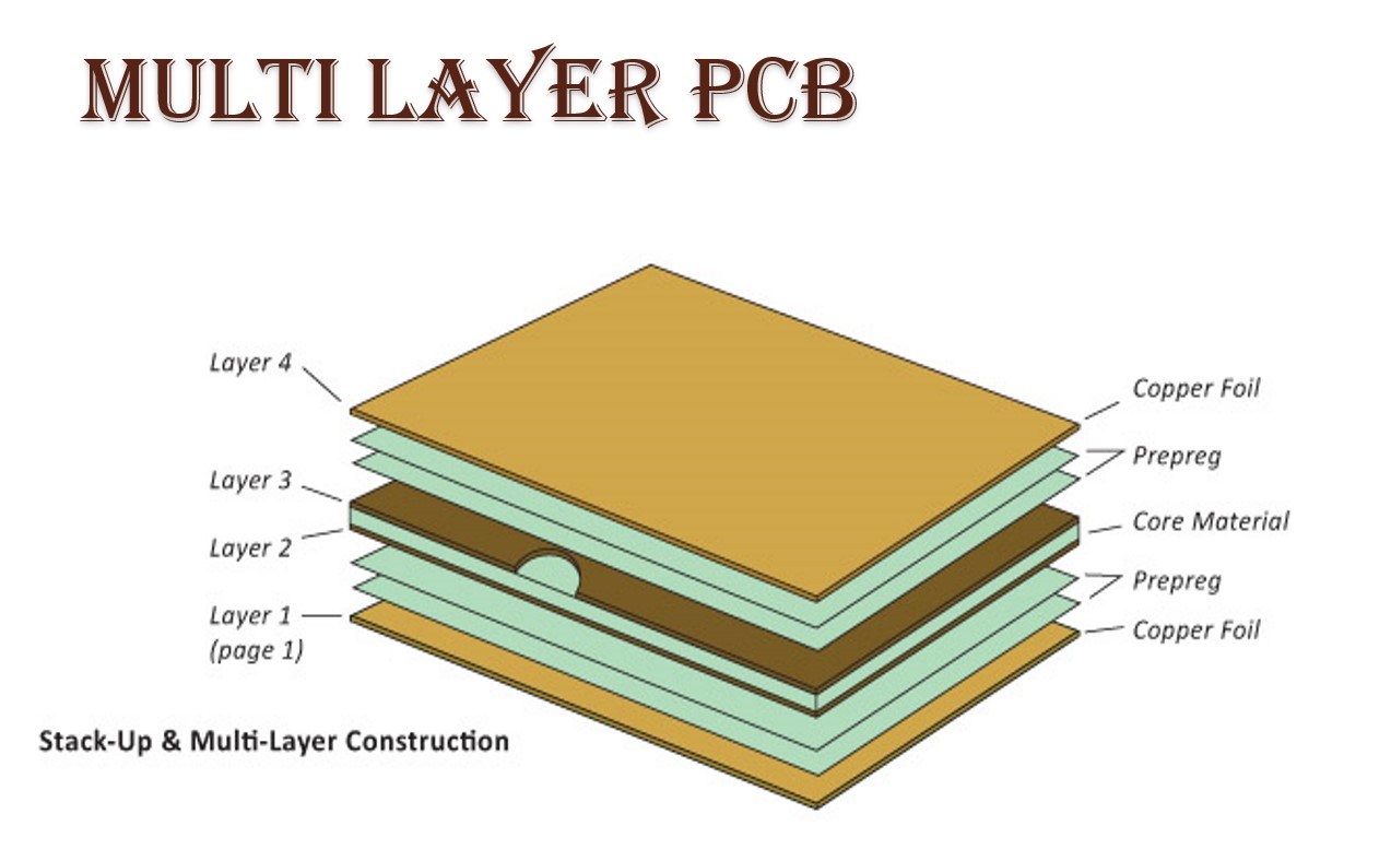
 MULTI LAYER PCB: Having more than two conductor pattern inside the board
To minimize the PCB board size
They are made by gluing (laminating) several double-sided circuit boards together with insulating layers in between.
FACT: Almost 100 layers can be made
MULTI LAYER PCB: Having more than two conductor pattern inside the board
To minimize the PCB board size
They are made by gluing (laminating) several double-sided circuit boards together with insulating layers in between.
FACT: Almost 100 layers can be made
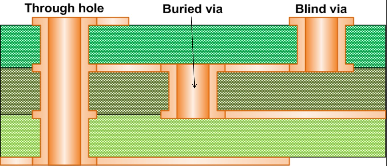
 The vias described in multi layer PCBs do not penetrate the whole board, all the time.
Blind vias connect one or more of the inner layers with one of the surface layers, without penetrating the whole board.
Buried vias only connect inner layers so you can’t see them by looking at the surface of the PCB.
The vias described in multi layer PCBs do not penetrate the whole board, all the time.
Blind vias connect one or more of the inner layers with one of the surface layers, without penetrating the whole board.
Buried vias only connect inner layers so you can’t see them by looking at the surface of the PCB.
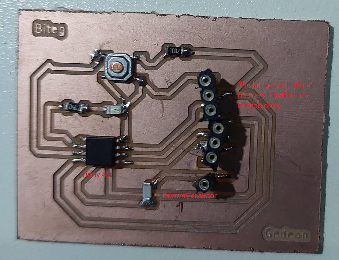
 Now to the assignment's question one:
STEP1: Installing the software that does the PCB design.
Now to the assignment's question one:
STEP1: Installing the software that does the PCB design.
INTRODUCTION:I considered using many other software, especially those recommended in the class like Eagle PCB.
However, since there is a licence issue i chose to use KiCad that is free. I will demonstrate how i intalled it below:
- I downloaded the installation file from: kicad.org/download/windows/
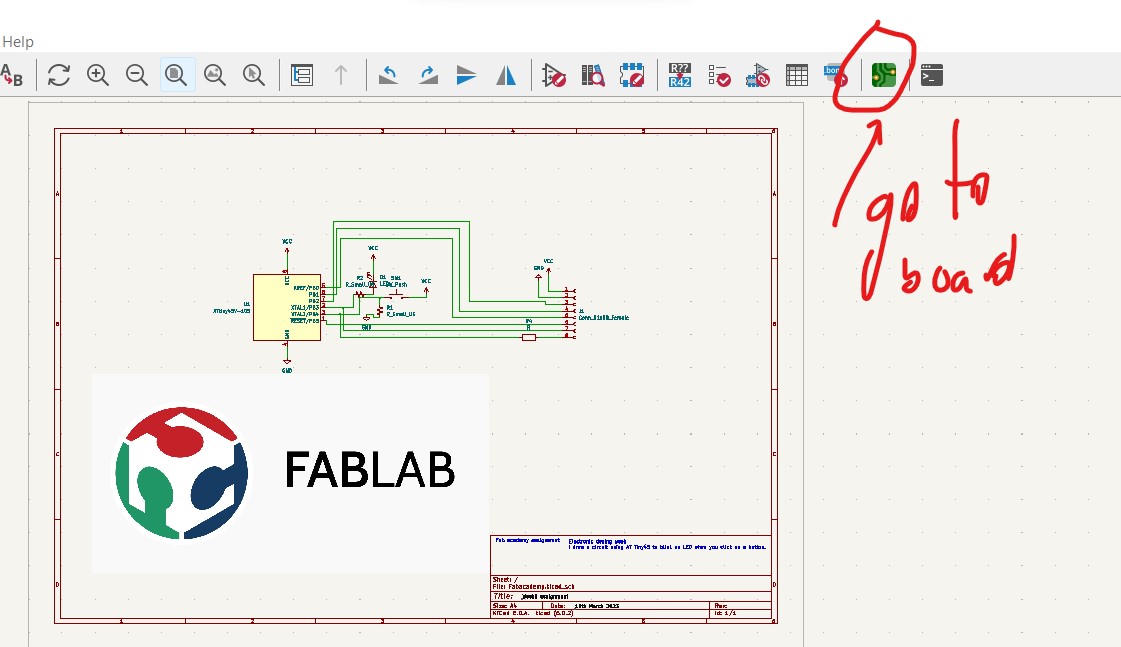
- After unziping and installing, i straight went to opening Kicad File>New Project>nameit
- I started with a schematid diagram
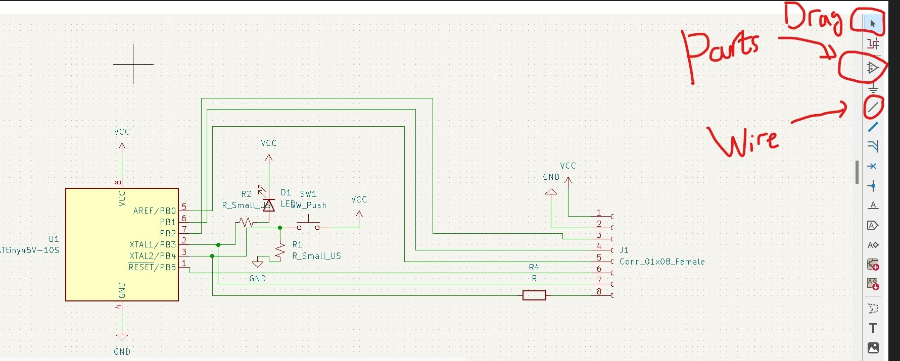
- i went on by fancying the design and edited the lablel
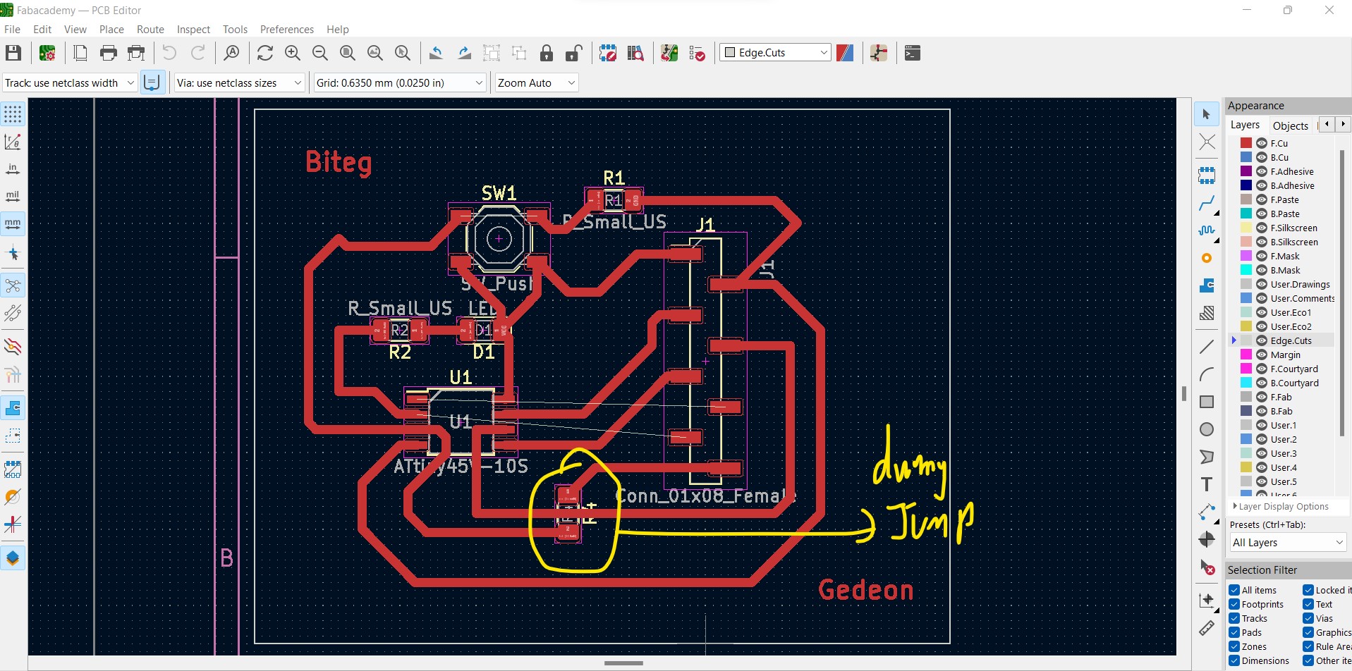
GOING TO THE BOARD AFTER ERROR CHECKS
Click on the switch to board, drag and drop componets into the given space.
 Since the Kicad software does not encourage the auto-trace way of doing things,
i had to manually route(add a wire) to each path.Plus we are supposed to use one side of the board.
As a consequence, there were two lines i couldn't wire without causing an error.
The trick is to add a 0Ohm resistor (dummy resistor) to allow crossing over the other line.
Setting the wire thichness also is importance as it results in the capacity to conduct electricity (resistance)
I uses 0.75mm as the thichness
Since the Kicad software does not encourage the auto-trace way of doing things,
i had to manually route(add a wire) to each path.Plus we are supposed to use one side of the board.
As a consequence, there were two lines i couldn't wire without causing an error.
The trick is to add a 0Ohm resistor (dummy resistor) to allow crossing over the other line.
Setting the wire thichness also is importance as it results in the capacity to conduct electricity (resistance)
I uses 0.75mm as the thichness
 Here i show which resistor is dummy
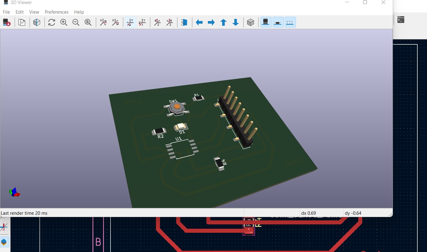
 The 3D View of the expected PCB:
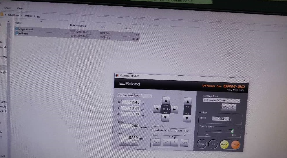
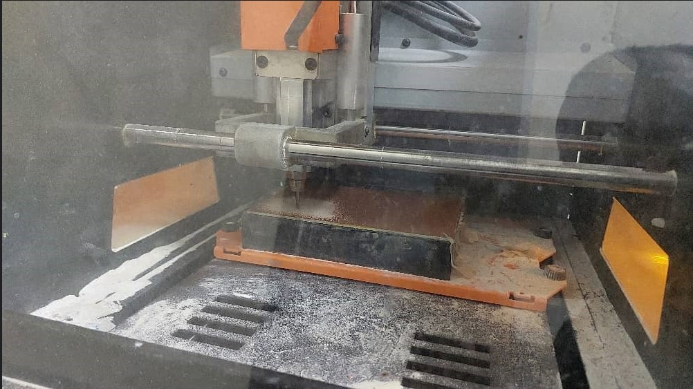
 The next steps:
Setup the machine
The next steps:
Setup the machine
 Print the board
 Clean it
 Solder components on and operate.
 The details of the last few steps are in the assignment of Week8_Electronic_production
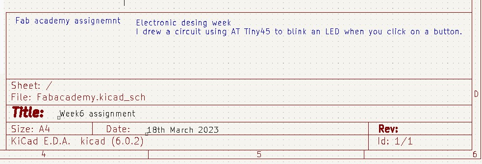
Files used
Schematic
Board
Traces in svg
Edge cuts in svg