6. Electronics Design
This week’s task is to design a development board to interact and communicate with an embedded microcontroller.
When I first started this assignment, I started to list all input and outputs I would need for my final projects and use those to design the board for this assignment. The list included multiple servo motor controllers, multiple temperature/humidity sensors, remote on/off switch among other things.
While doing the research on how to design a board with all these functions and components, I became overwhelmed with the magnitude of the task. The number of decisions necessary to accomplish this task was immense and beyond my current electronics knowledge, so I decided to take a step back and reevaluate my goals.
Development Board
-
I rewatched Neil’s lecture for the week and reread the assignment to realize that I was overcomplicating the assignment. The assignment wasn’t a fully functional board with inputs and outputs, but rather to design a simple development board.
-
I then realized that I didn’t have a solid definition of what a development board actually entailed, so I turned to my new friend, ChatGPT, and asked it the question “In electronics, what is definition of a development board?”
- Here is the response:
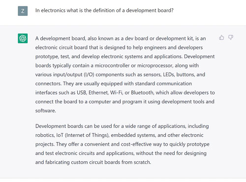
- Here is the response:
-
With a better understanding of my assignment, I turned to Adrian Torres’s XIAO RP2040 board as a reference to begin the task of designing my own development board.
-
I’m going to design a board based on the SeeedStudio XIAO RP2040. To simulate it, I’m using the Raspberry Pi Pico Simulator on Wokwi because it also uses the RP2040 microcontroller.
KiCad
-
The first task was to install both the fab library and the SeeedStudio XIAO library in KiCad. After a few missteps, I got the XIAO library installed. Long story short, I was using the wrong folder button when trying to add the library file. See picture.
-
When it came time to install the fab library from GitLab I received a message that my KiCad build was out of date (6.0.8) and I needed to update. I downloaded and installed KiCad 7.0 and got started. I installed the fab library and the SeeedStudio XIAO library before I began.
-
As I mentioned earlier, I used Adriann’s Fab-XIAO board as an example from which to learn about development boards. I downloaded and opened the KiCad version of the Fab XIAO board to see how it was designed and learn my way around KiCad a little more. I also used the getting started guide on the KiCad 7.0 homepage and found it also helpful.
-
Once I had the schematic and PCB design in KiCad and the pinout for the XIAO RP2040 all pulled up on my various screens I meticulously traced them around the board to see how the boards worked. I also changed some connections in the schematic to see how the updates would work in the PCB Design. That allowed me to better understand how to make a similar design in KiCad.
-
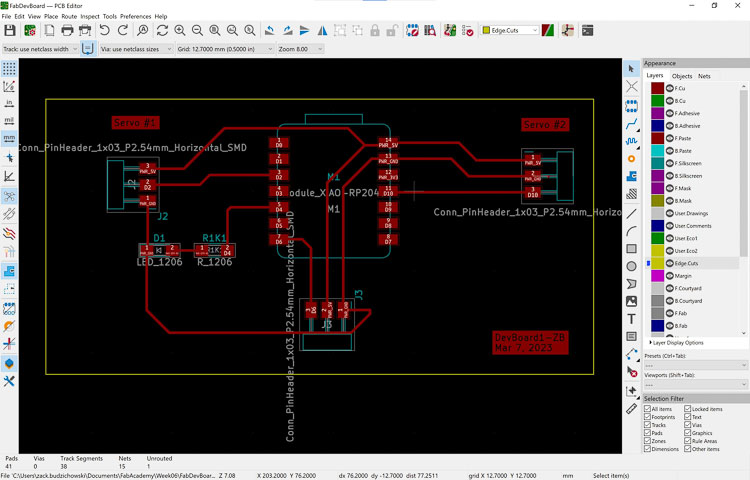
My board is going to have three connections. Two for servos and one for a temperature sensor. Each of the connectors will have three pins. I will also include an LED for testing along with the requisite pull down resistor.
-
I opened KiCad and started with the schematic view and inserted:
- 1x-XIAO RP2040 (Module_XIAO-RP2040);
- 3x-(Conn_PinHeader_1x03_P2.54mm_Horizontal_SMD) connectors;
- 1x-(LED_1206) LED; and
- 1x-(R_1206) 1000 ohm resistor
-
Then it was time to label everything according to the pinout on the XIAO and use corresponding labels on the connected components. This is necessary to make the transition to the PCB editor easier. Once the labels are correct, the PCB editor matches the corresponding pads to assist with making the traces.
-
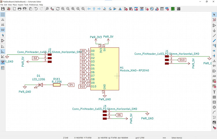
Here is the finished schematic
-
Now to the PCB Editor and placing all the footprints on board.
-
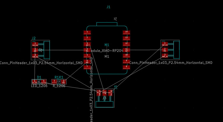
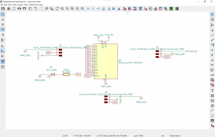
I have some problems that I need to go back and fix in the schematic. I have too many crossover traces in the board that would make routing a nightmare, so I can go back and tweak the schematic to make it easier. I got ahead of myself when I said the schematic was finished. Engineering is an iterative process, so I iterate…and iterate some more. Now here is the finished schematic....
-
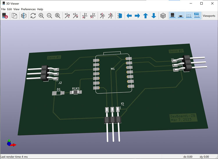
And here is the final PCB drawing with traces along with the 3D view.
-
After quite a bit of iterative design along with reading tutorial and trial and error, I learned how to do the following:
- Place items in the schematic and label them according to the pinout of the XIAO
- Switch to the PCB editor and add the footprints for the components that correspond to the item in the schematic.
- Routing was quite tricky at first, but I think I have the hang of it now. It was important to layout the components on the board to minimize the length of the traces by placing the components as close to the pin they connected to as possible.
- The most important useful skills I learned was how to move the objects around with fine movement by holding down the control key as I used the mouse.
Link to my files for the week.
Group Assignment
Link to our group assignment.