6. Embedded Programming
Learning outcomes
- Identify relevant information in a microcontroller datasheet.
- Implement programming protocols.
Objectives
-
Linke to the group assignment page
-
Documentd what was learned from browsing through a microcontroller datasheet.
-
Program microcontroller board(s) to interact and communicate
-
Describe the programming process(es) used
-
Include source code
-
Inclue‘hero shot(s)’
Link to the group assignment page
https://fabacademy.org/2021/labs/vancouver/students/terrence-carew/assignments/week04g.html
This week i decided to used the attiny412 to develop my hello button + LED board.
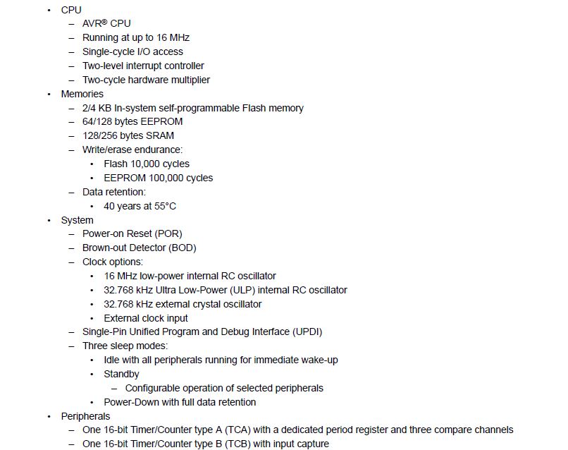
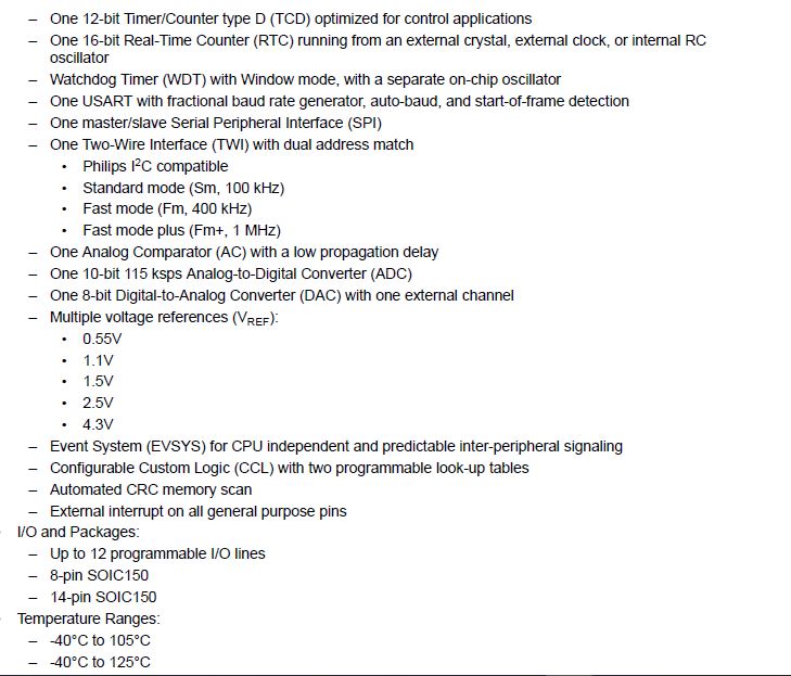
** The main FEATURES of the attiny412 are as follows: **
The following picture shows a pinout of the 8PIN SOIC
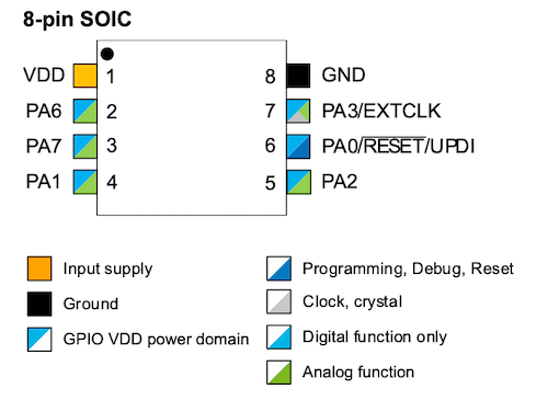
Below is a basic identification of the pins
- VCC-Power supply
- GND - Ground
- PA - Port Pins
- UPDI - Through this pin you can program the board via a UPDI connection
- RESET -Through this pin you can reset the microcontroller
- EXTCLK - External Clock Where you can connect this pin to an external clock, such as a resonator
Recommended Pins
-
For prototyping w/out breadboard: Two 1x6 pin male pin header for the rows of pins on the sides (in picture, 1x3 in black, for the I/O pins, 1x3 green and red for ground and vcc pins - colored pin header kits available as option)
-
For use with breadboard 2 1x6 “machined” pin headers are recommended. The full-size 0.1” header deforms the clips in the breadboard, making the holes it is plugged into unreliable when using things with smaller pins.
-
A 1x6 pin header for the serial port (standard FTDI pinout) - I recommend 90-degree angled male pin header.
-
A 1x3 pin header for UPDI programming - I find straight pin header more convenient on breadboard (so the cable doesn’t get in the way as much), and angled header more convenient if not using breadboard (for the same reason).

Memory Highlights:
-
The Flash memory is 4KB and is the space that is available for the storage of the program to be uploaded using the UPDI
-
The EEPROM ( Electrically Erasable Programmable Read-Only Memory), is 64/128 bytes used to store small amounts of data
-
The SRAM (Static Random Access Memory) is 128/256 bytes. This is the memory that is used to hold the variables and functions in memory while the chip executes its tasks.
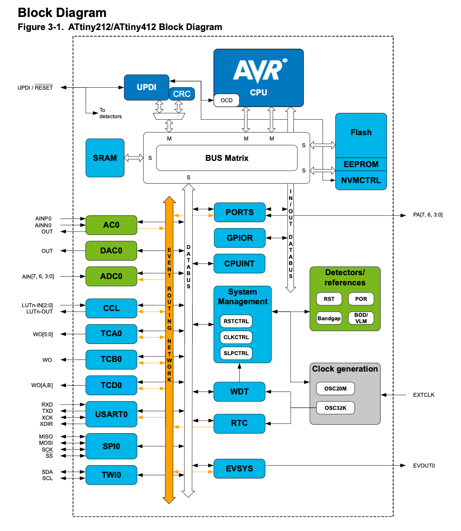
The attiny412 block diagram shows what’s inside of the microcontroller.
AVR Microcontroller:
AVR also known as Advanced Virtual RISC, is a customized Harvard architecture 8 bit RISC solitary chip micro-controller. It was invented in the year 1966 by Atmel. Harvard architecture signifies that program & data are amassed in different spaces and are used simultaneously. It was one of the foremost micro-controller families to employ on-chip flash memory basically for storing program, as contrasting to one time programmable EPROM, EEPROM or ROM, utilized by other micro-controllers at the same time. Flash memory is a non-volatile (constant on power down) programmable memory.
AVR Microcontroller Architecture:
AVR microcontrollers’ architecture was developed by Alf-Egil Bogen and Vegard Wollan. The name AVR is derived from the names of the architecture developers of the microcontroller. The AT90S8515 was the foremost micro-controller which was AVR architecture based; on the other hand the foremost micro-controller to strike the commercial marketplace was AT90S1200 which was launched in the year 1997.
The SRAM, Flash and EEPROM all are incorporated on a single chip, thereby eliminating the requirement of any other external memory in maximum devices. Several appliances comprise of parallel external bus alternative, so as to add extra data memory gadgets. Approximately all appliances, except TinyAVR chips comprise serial interface, which is used to link large serial Flash & EEPROMs chips.
ARM Microcontroller:
ARM is the name of a company that designs micro-processors architecture. It is also engaged in licensing them to the producers who fabricate genuine chips. In actuality ARM is a 32 bit genuine RISC architecture. It was initially developed in the year 1980 by Acorn Computers Ltd. This ARM base microprocessor does not have on-board flash memory. ARM is particularly designed for micro-controller devices, it is simple to be trained and make use of, however powerful enough for the most challenging embedded devices.
ARM Microcontroller Architecture:
The ARM architecture is a 32 bit RISC processor developed by ARM Ltd. Owing to its power-saving attributes, ARM central processing units are prevailing in the mobile electronics marketplace, where less power expenditure is a vital design aim. ARM architecture comprise of the underneath RISC elements:-
- Maximum single cycle functioning
- Constant 16×32 bit register file.
- Load or store architecture.
- Preset instruction width of 32 bits so as to simplify pipe-lining and decoding, at minimized code density.
- For misaligned memory access there is no support.
Getting aquainted with arduino programming using the arduino IDE(integrated development environment).I downloaded the arduino IDE from the following website :
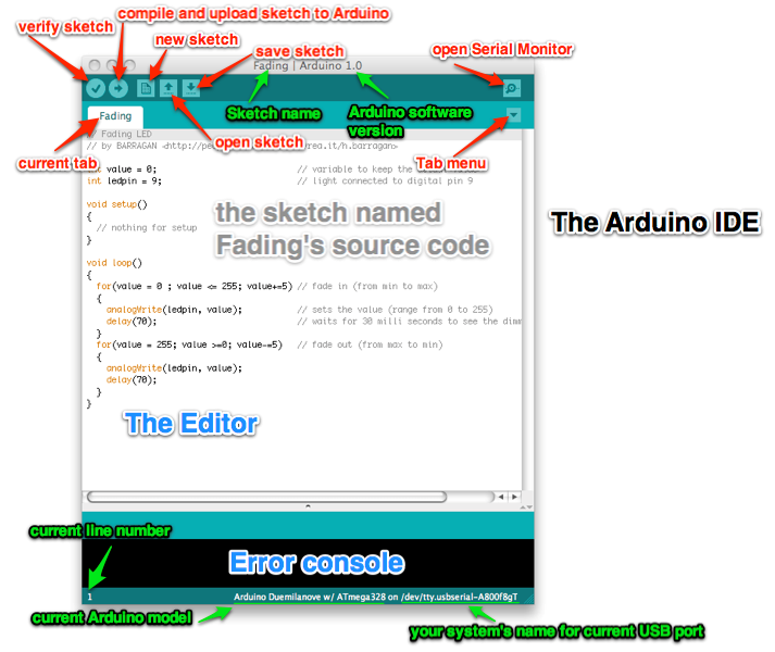
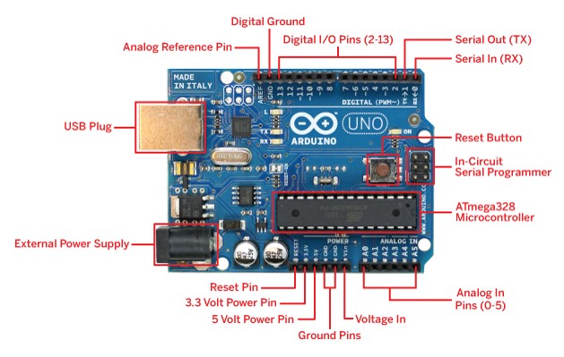
I would be using the arduino uno to test the blink code from the arduino ide.Below is a picture of the main pins and ports identified on the arduino uno.
There is a bare minimum that must be adhered to when writing any code using the arduino IDE as shown in the picture below which includes the void setup and void loop as shown in the image below.

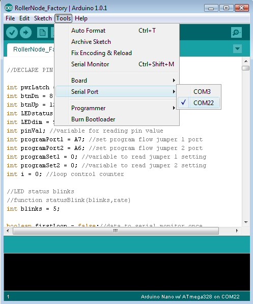
Selecting the right Port is critical for uploading the program and may only appear when a device is connected to a serial port.
Find your port > Device manager -> ports
Select your port > Arduino -> tools -> Serial Port
BASIC DEFINITIONS
pinmode()
Syntax :
pinMode(pin, mode) Parameters : pin: the number of the pin whose mode you wish to set mode: INPUT or OUTPUT
digitalwrite()
Syntax :
digitalWrite(pin, value) Parameters : pin: the pin number value: HIGH or LOW
Delay()
Description Pauses the program for the amount of time (in miliseconds) specified as parameter. (There are 1000 milliseconds in a second.) Syntax : delay(ms) Parameters ms: the number of milliseconds to pause (unsigned long)
semicolon;
used to end a statement eg.delay(1000); // wait for a second
The sketch was uploaded to the arduino uno as follows:

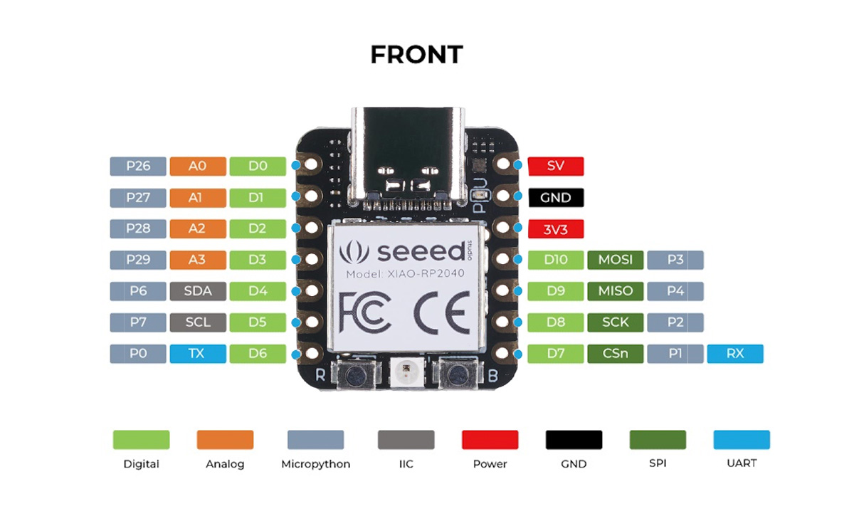
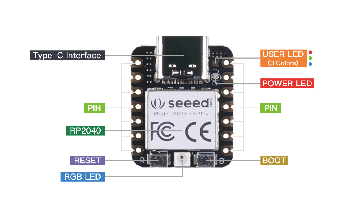
To get a further insight into programming and how electronics work I started looking at the seeed XIAO RP2040.
Components Used
1.Seeed Studio XIAO RP2040 x1
2.Resistor(1K)
3.Light Emitting Diodes(3)
4.potentiometer
5.Breadboard
6.Jumper Wires
7.USB Type-C cable
Information obtained from the seeed XIAO RP2040 datasheet
Soldering the pin headers(pic)
Setting up the XIAO RP2040 with Arduino
Step 1
I navigated to file > preferences and in the additional boards manager url’s paste the following link.
https://github.com/earlephilhower/arduino-pico/releases/download/global/package_rp2040_index.json
Step2
Open the arduino application and add the XIAO PR2040 board package to the arduino IDE.
Step3
Blink code for seeed XIAO RP2040
void setup() {
    // put your setup code here, to run once:
    pinMode (25, OUTPUT) ;
}

void loop() {
    // put your main code here, to run repeatedly:
    digitalWrite(25, HIGH) ;
    delay (1000);
    digitalWrite(25, LOW) ;
    delay(1000);
}
This is the code to control an LED via a potentiometer for seeed XIAO RP2040
const int sensorPin = A0;
const int ledPin =  27;

void setup()
{
  // declare the ledPin as an OUTPUT:
  pinMode(sensorPin, INPUT);
  pinMode(ledPin, OUTPUT);
}

void loop()
{
  // read the value from the sensor:
  int sensorValue = analogRead(sensorPin);
  // turn the ledPin on
  digitalWrite(ledPin, HIGH);
  // stop the program for <sensorValue> milliseconds:
  delay(sensorValue);
  // turn the ledPin off:
  digitalWrite(ledPin, LOW);
  // stop the program for for <sensorValue> milliseconds:
  delay(sensorValue);
}
References
https://wiki.seeedstudio.com/XIAO-RP2040-with-Arduino
https://how2electronics.com/getting-started-with-seeed-xiao-rp2040-with-projects/
https://www.electronicshub.org/microcontrollers/