Electronics Production
This week, the mission is to create a circuit programmer that includes a microcontroller by milling and stuffing the PCB by testing it, and then possibly trying other PCB processes.
The work of this week was not easy as it is the first that I make a PCB, but with our instructors we were able to carry out our project.
To be explicit and facilitate the understanding of our work we decided to divide our work into several parts namely:
- Design of the png file with Eagle;
- Configuration and export of a file with the MODS module;
- Milling the circuit with the Modela MDX50;
- Welding of the various components;
- FabISP configuration;
- And test.
File design with Eagle
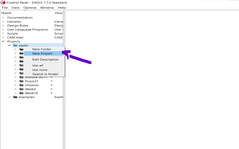
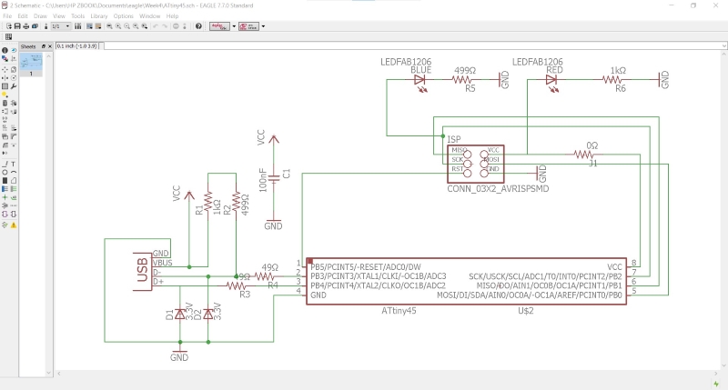
To be able to design the circuit on Eagle we needed the tutorial. We had already installed Eagle but you can find it on this site. Without further ado we will open our Eagle. In order to show how to create a project on Eagle, we saw fit to illustrate this with the images above.
Project creation image.
Project creation on eagle
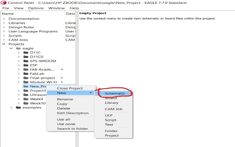
Component Selection
To be able to wire the circuit as it should be we needed this tutorial. Thus, before starting the wiring we will go to select the desired components.
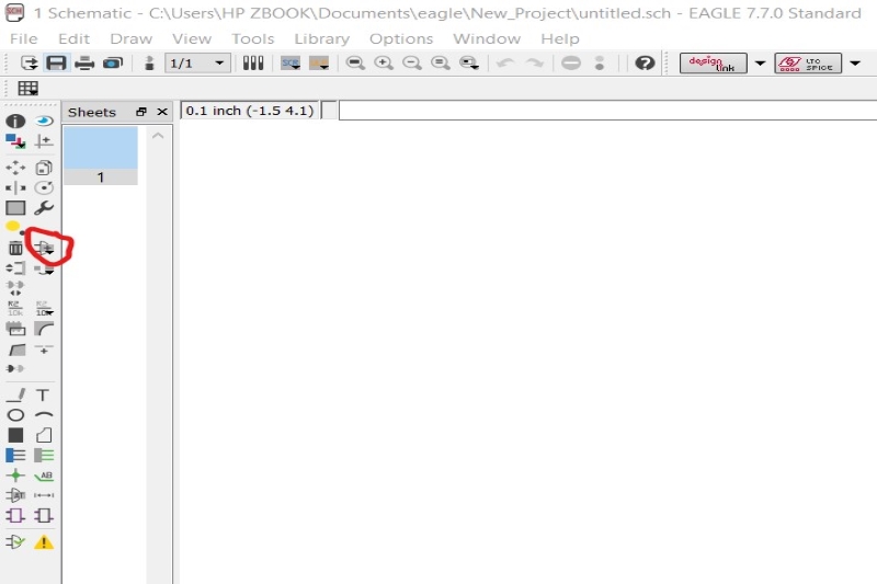
After clicking on schematic (explained above) we have this window that opens. Then you click on the icon circled in red. This one sends you to the library of the different Lab, you unfold and choose your component.
We will describe the whole process through the images below.
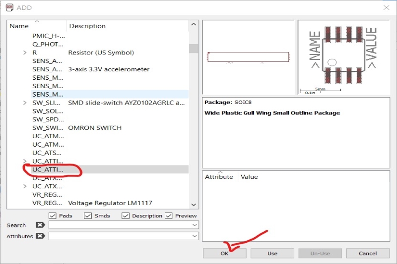
This process is the selection of a single component but it is the same for the others.
The photos above represent the selection of components to be able to carry out the project. This process is the selection of a single component but it is the same for the others.
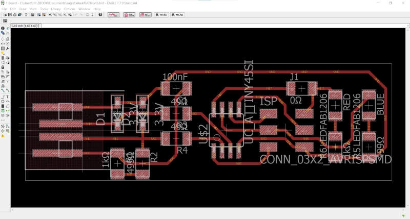
Classification of components and trace
This step consists of classifying all the components of the circuit in order to trace the route path. To better understand this, let's look at the images below.
The photos above represent the selection of components to be able to carry out the project. This process is the selection of a single component but it is the same for the others.
Classification of components
Exporting the file
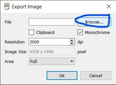
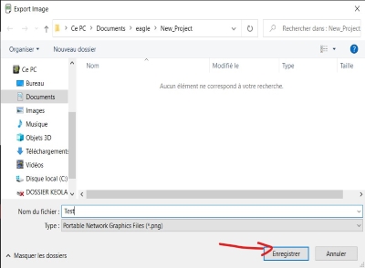
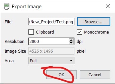
In this part we will export the file in order to be able to do the milling with Modela MDX50. To be able to work, the file must be exported in png image format. To do this we will click on File-->Export-->Image. One click on image in the small window check Monochrome, set the resolution (I set it to 2000dpi), then click on Browsers to save the image and finally OK. The images below represent the exportions of the image.
Image exporting the file to Eagle
Clicked in the part circled in blue
Named the folder clicked on save
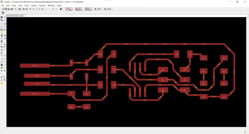
MODS
Once the file export us create the route path so that the machine can perform the milling.
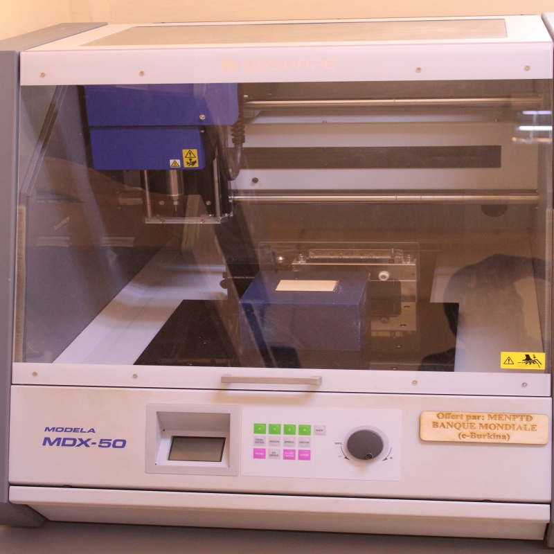
Modela MDX-50
Formilling we used Modela MDX50 from our FabLab. Highlight the specifications of our machine above.
Specifications
Acceptable materials: Resins such as chemical wood and modeling wax (metal not supported)
Operating range: X : 15,80 pouces (400 mm), Y : 12,00 pouces (305 mm), Z : 5,315 pouces (135 mm);
Table size: W:15.80in (400mm), D:12.00in (305mm);
Axis drive: Stepper Motor;
Feed rate: XY: 0.3in to 141.7 in/min (7 to 3600mm/min),Z: 0.3 to 118.1 in/min (7 to 3000 mm/min);
Mechanical resolution: 0.01 mm/step (0.39 mil/step; half step)
Tool chuck: Collet;
Power requirements (VAC/A): AC 100 to 240 V ±10%, 50/60 Hz, 1.2 A, (Overvoltage Category: II, IEC 60664-1).
Once the configuration is finished on Aspire we will configure the machine for engraving and cutting.
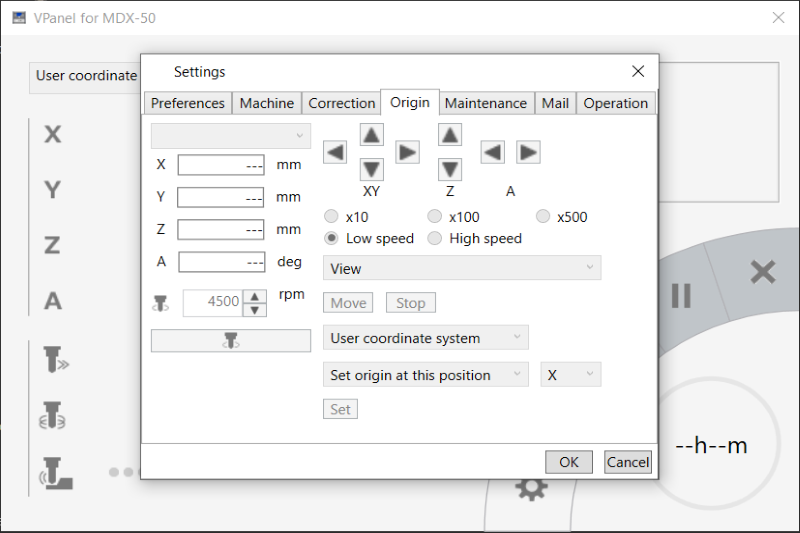
Modela MDX50 is the machine we have in our LAB. It is she who will allow us to have our PCB. As machine control software we will use VPanel for MDX-50.
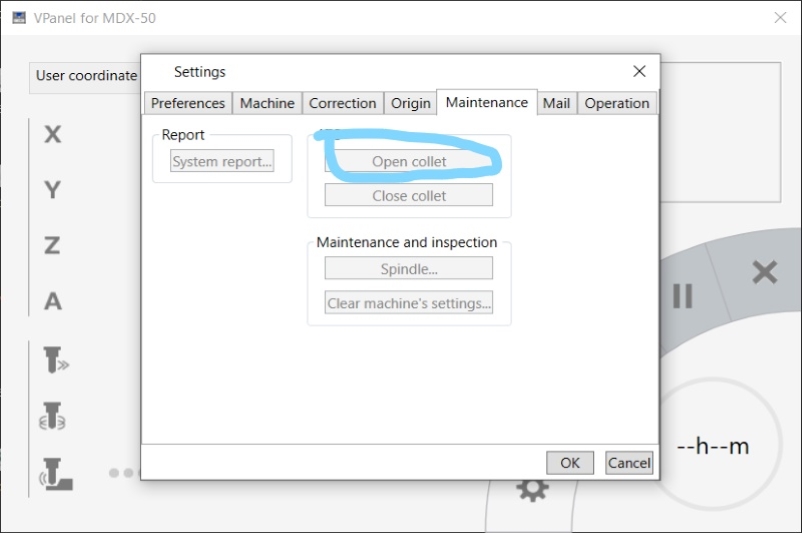
Before I started I found that there was a wick of 1/32inch on the machine. I had to change it into a 1/64 inch wick to do the engraving. For this I opened VPanel for MDX-50 and in parameter there is maintenance and once in maintenance I click on Open collet to remove the wick and change. After change, I click close collet.close collet.
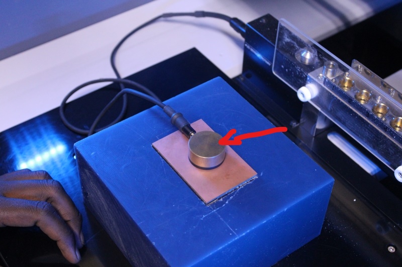
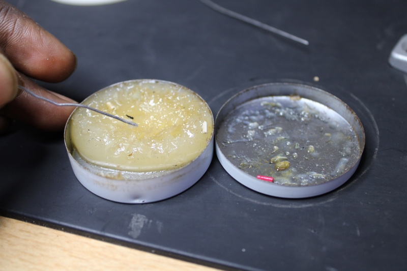
After the maintenance I measured the Z axis. This is done with a measuring copper tool.
Manual control of the machine
The arrow indicates the measurement tool
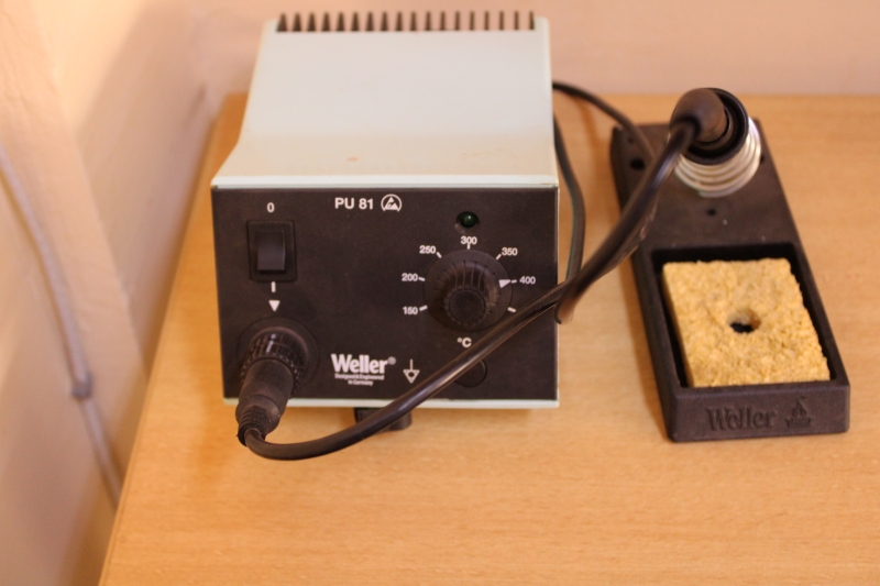
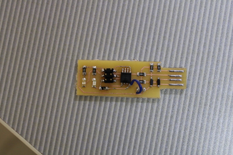
Solder
In this part I will weld the different components on the pcb above. For the welding I used a welding machine, the off temperature channelizer and a vacuum cleaner (to suck the smoke release during welding). The soldering went well because I didn't encounter any particular problems.
This image shows my final circuit after welding.
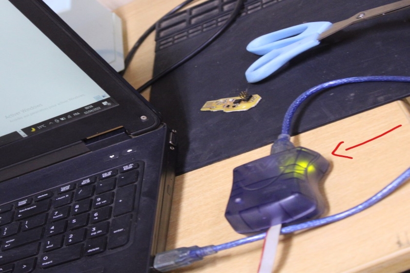
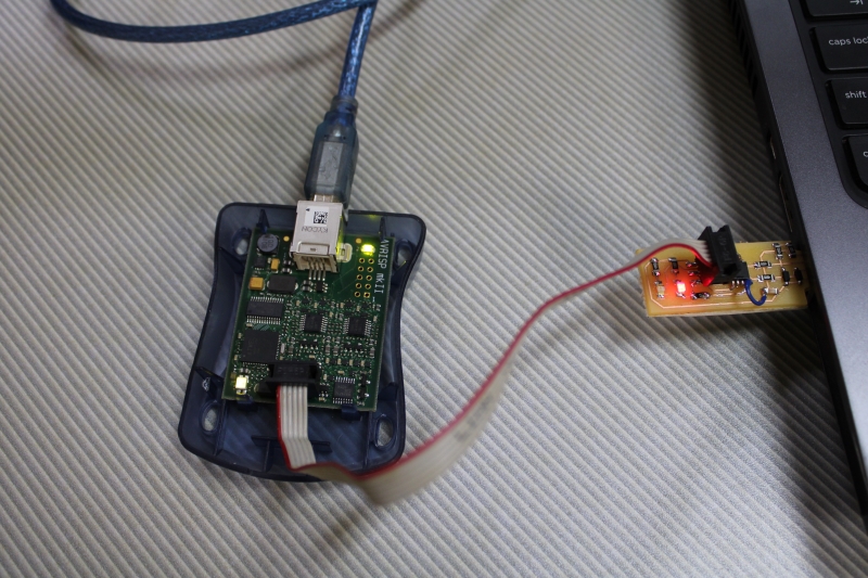
Configuring USBTiny
In this part, I configured my circuit to become the USBTiny so that I could use it. To do this, you must first install certain software and drivers. So I needed this tutorial before I could do the different installations.
Once the installation of the different drivers was complete we continued to follow the instructions in this tutorials in order to complete the process. The image above shows the connection of our AVRISP mkII and my circuit.
Image by AVRISP.
Connecting USBTiny with Avrisp mkII
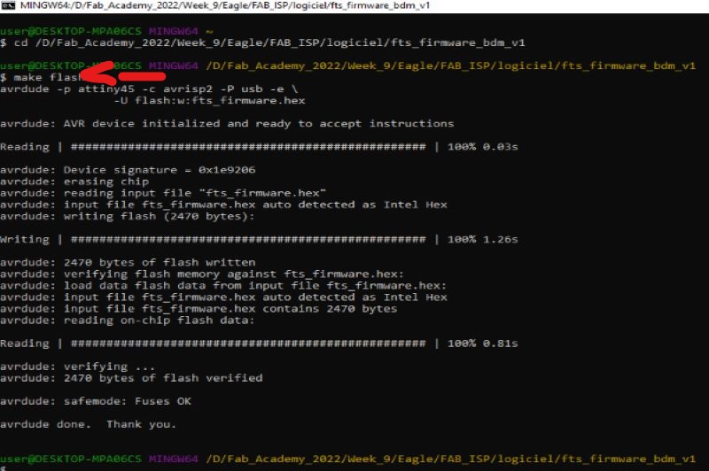
Make flash
According to the process after the connection we have to type in the terminal Git bash Make flash in order to erase the target chip and program the flash memory with the contents of .hex.
Make fuses
The make fuses allow you to skip the reset fuse.
Final
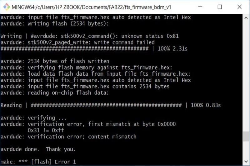
The process is very well finished but still I encountered a lot of problem since it is a first.
Difficulties and problems encountered
In this part, I have highlighted the different problems and difficulties I encountered during this mission. As I wrote at the beginning of the mission, this is my first time designing an electronic circuit. However, with the help of my instructor I was able to carry out my mission. It wasonly an immense joy but a satisfaction to have accomplished this mission.
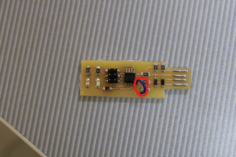
The major problem I encountered was while running Make flash. When I type make flash I have an error that appears. I did more than 24 hours trying to understand the error. And finally I checked my circuit and I realized that I had skipped a path on the circuit. To remedy this, I used a simple wire to join the two paths. The circled part in the photo represents the wire.