Electronics Design
Hero Shots
Click Here for Our Group Assignment
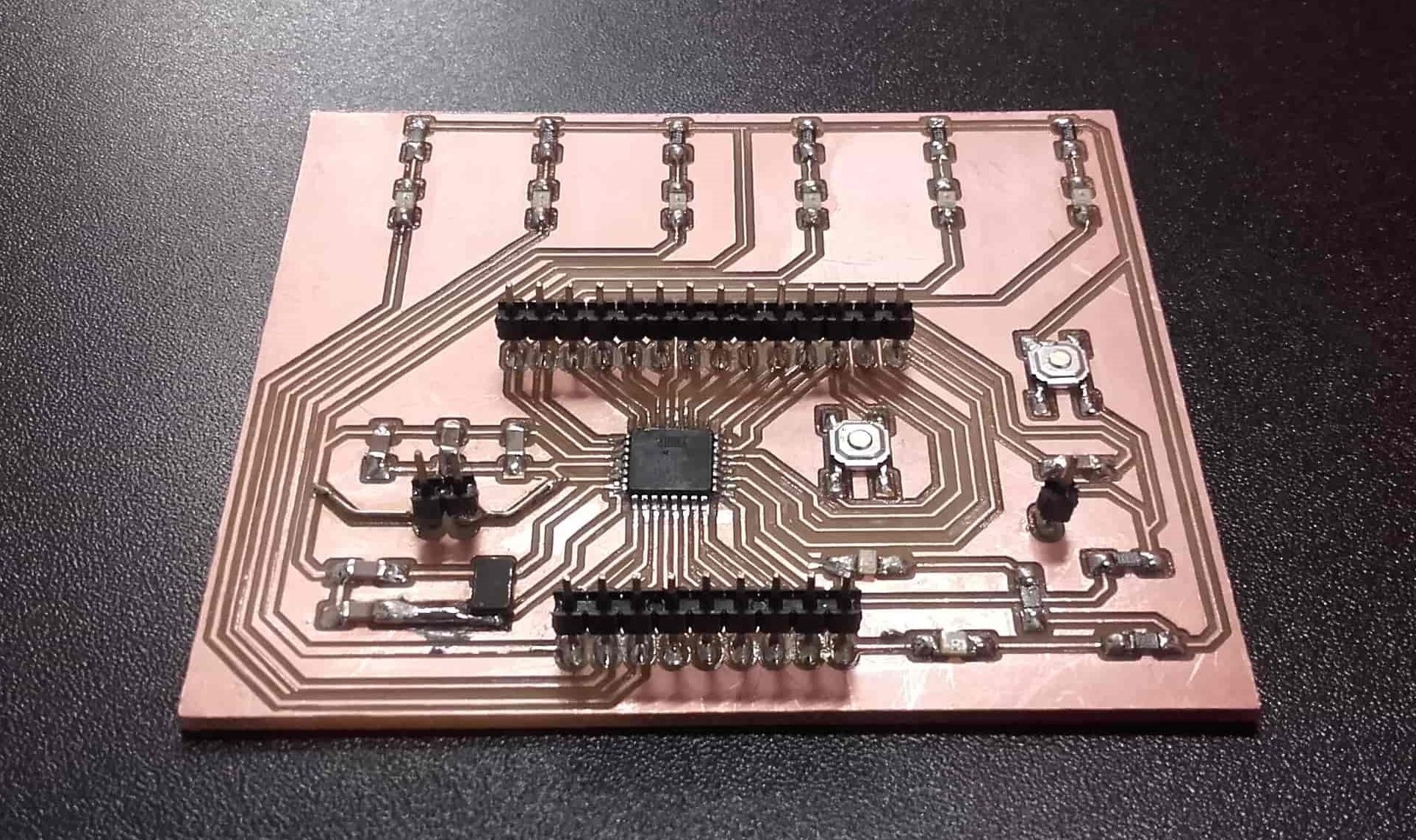
My Satshakit PCB
File Downloads From This Week
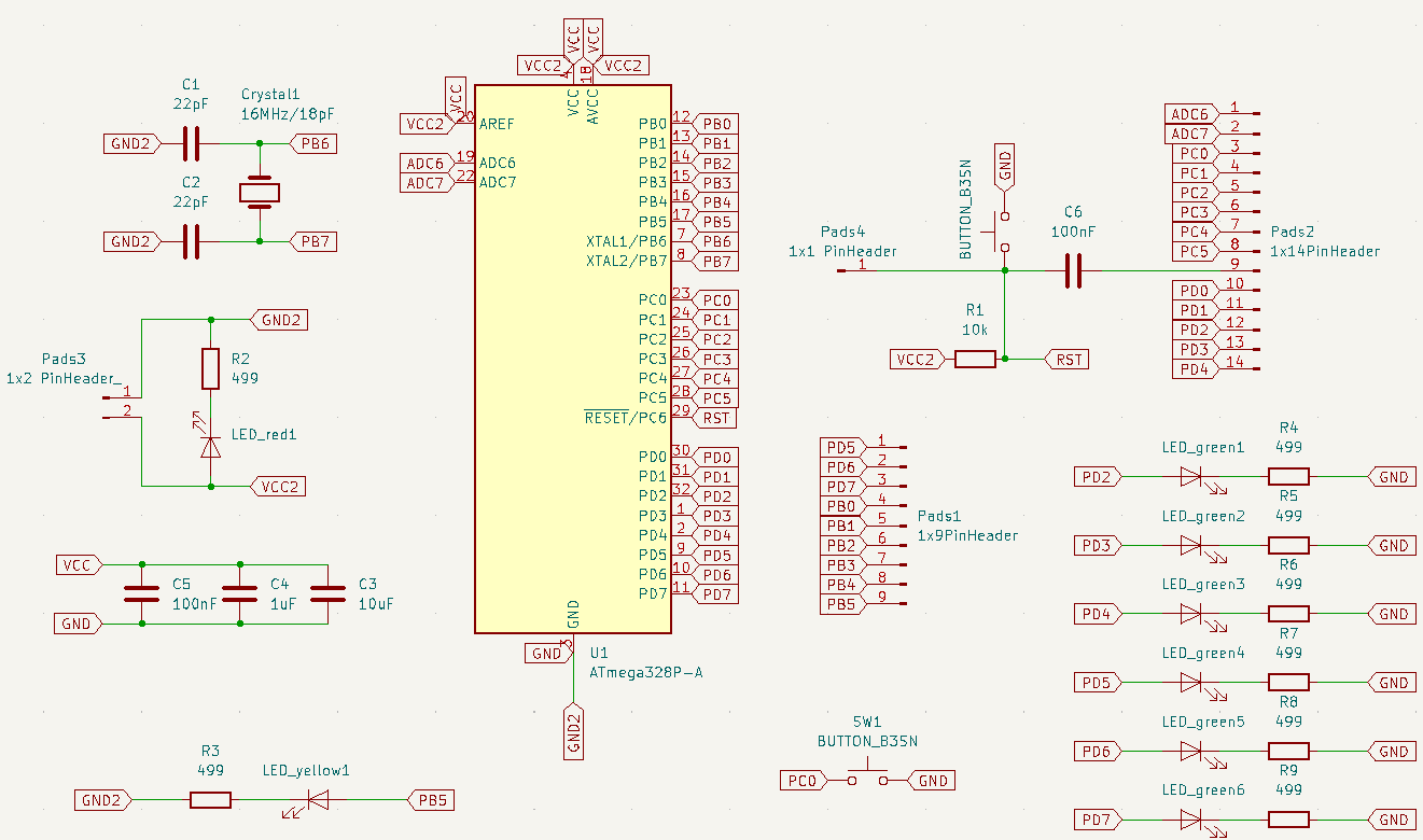
Schematic
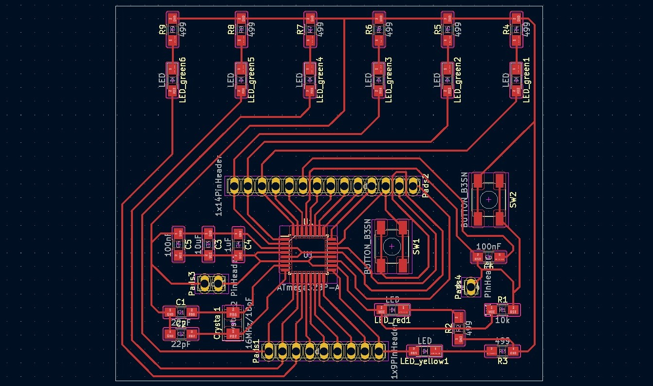
Blueprint
Initial Reaction
I am officially back in the world of "I don't know what the hell I am doing or why I am doing it" 😅. I think I understand the components and the math behind them, but in my experience, there's a big gap between theory and practice when it comes to electronics. I have never designed a PCB before, and have very little experience making circuits at all, but I am excited to learn more. Electronics is a big part of my field so I need to get comfortable with it. The group assignment this week is to use test equipment in the lab to observe a microcontroller circuit board during operation; and the individual project is to redraw an echo-hello-world board and to add at least a button and an LED to it.
After Local Workshop
This week, Ahmed took us step-by-step through the electronics design workflow. Using KiCad, he walked us through the process of how to create a schematic that defines the logical connections in the circuit and then to generate from that, a blueprint to define all of the physical placements and connections. He also showed us how to access the Fab libraries in KiCad so we can use the footprints for the specific components that are available in the lab. I can only imagine how much time and effort that saved us so I appreciated it. Looking forward to getting started.
Electronics CAD
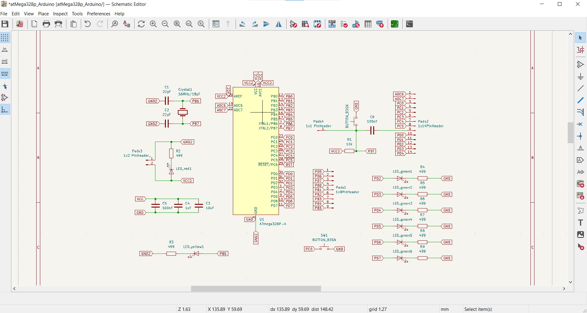
Making the Schematic
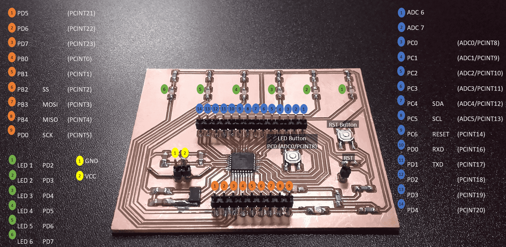
Satshakit
We have been encouraged to try to make these weekly projects relevant for our final projects, so I sat down with Marcello and discussed my project, what I would like it to do, and what I will need to be able to accomplish it. He told me that I would basically just need an Arduino Uno, and advised me to attempt my own satshakit. Originally designed by Daniele Ingrassia, the satchkit, is an open source board that is 100% compatible with the Arduino IDE and libraries. This board is definitely more ambitious than I would have attempted this week, but I will feel great if I am able to pull it off! I was also worried that it might not count for this week's assignment, but he assured me that it would as long as I added at least an LED and a button to it. I decided to add a button and six LEDs for reasons that will become apparent in my final project soon 😉. Using a very difficult to read schematic from another version of the satshakit as a reference, I set out to build my own.
KiCad
I opened up KiCad, and created a new project.
Adding Components
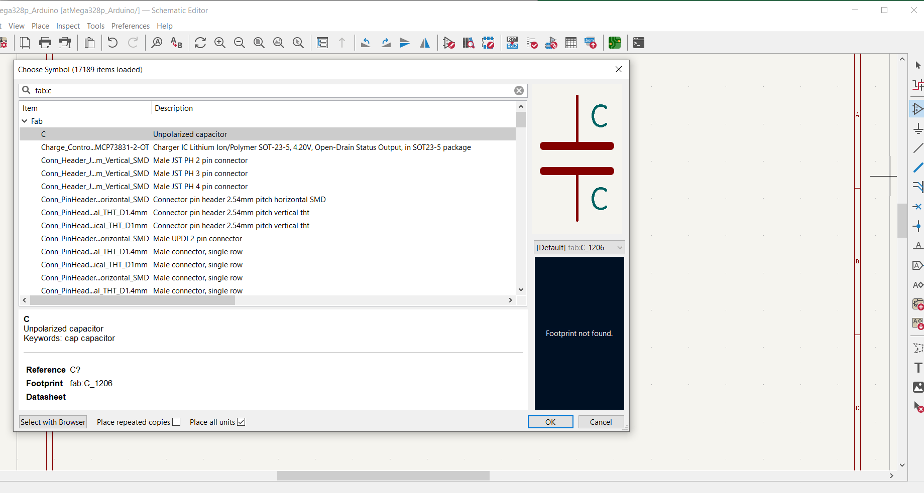
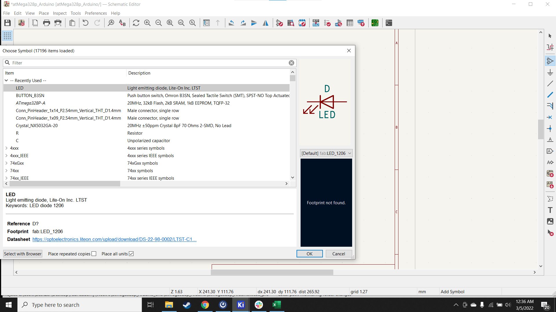
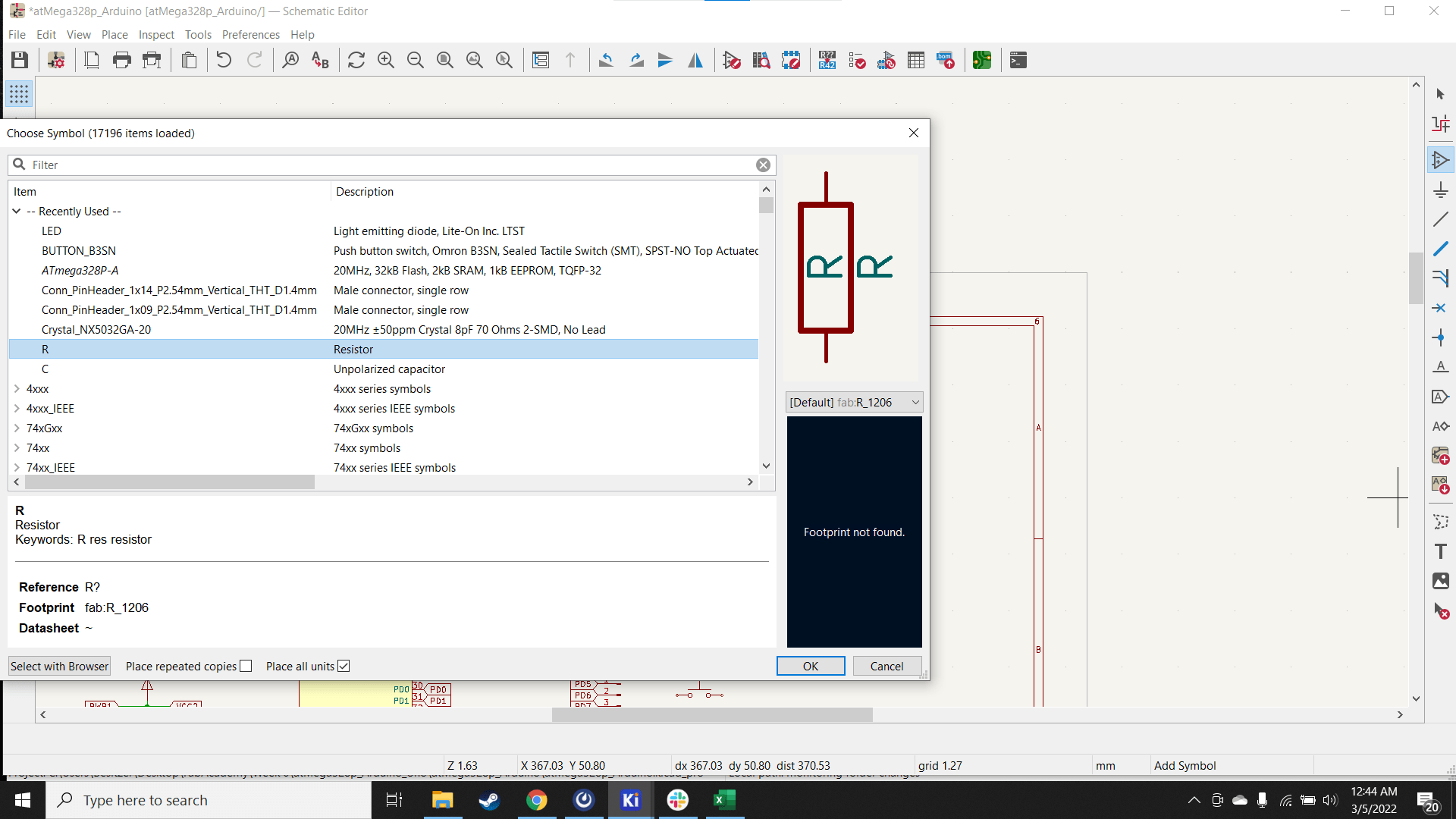
I added the components from the BoM using the Add a Symbol tool, always ensuring that I was selecting from the Fab library so I would be using components that are actually available to me.
Renaming
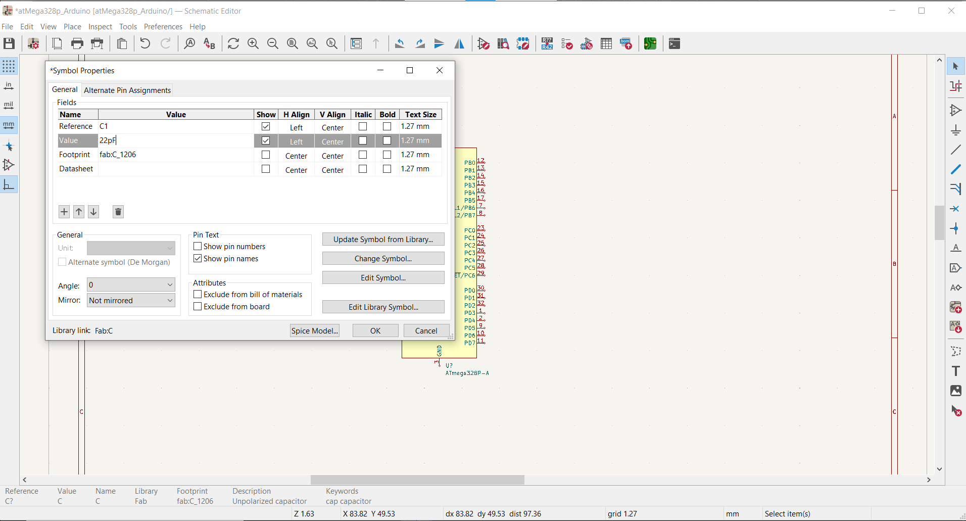
Then I assigned meaningful names and proper values to the components by double-clicking them.
Crystal Drama
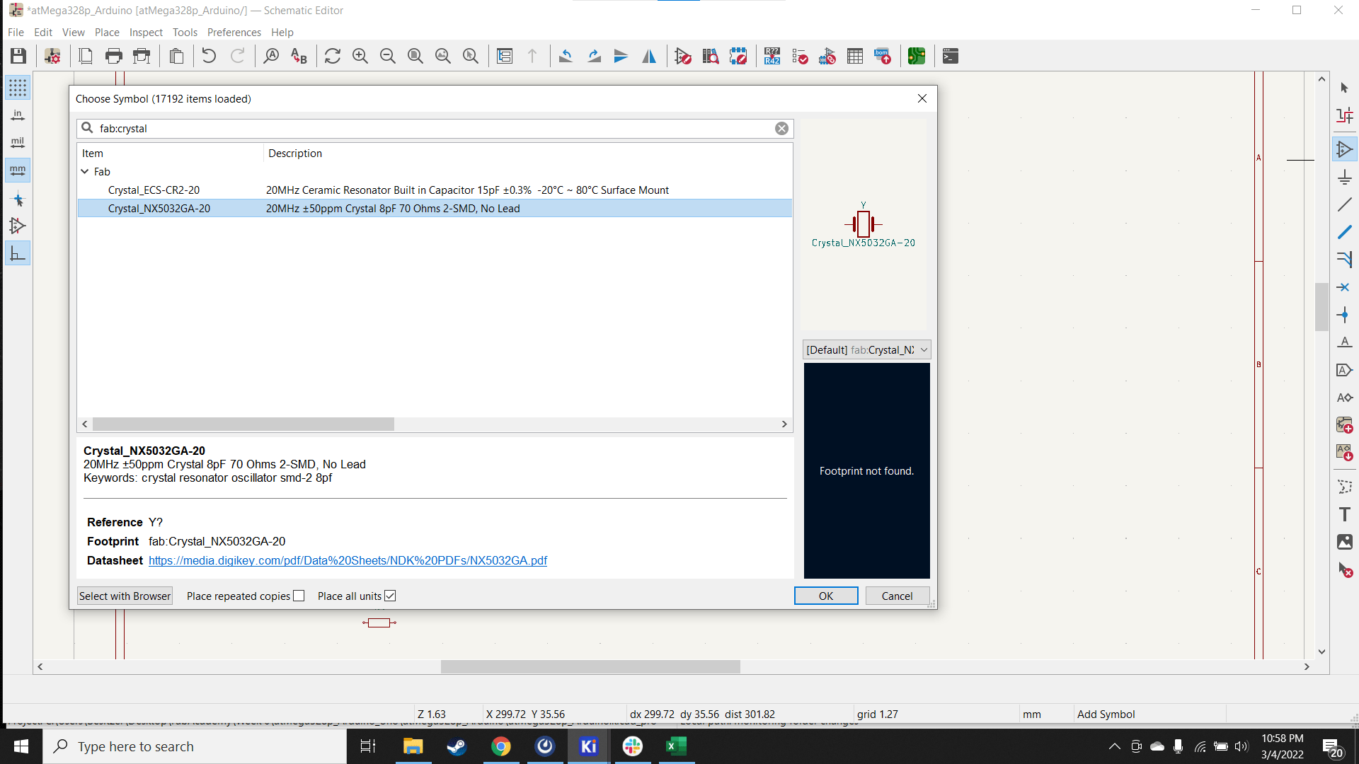
The Fab library only has 20 MHz crystals, and I needed a 16 MHz one...I knew we had them in the lab, so I double-checked the datasheets to make sure they had the same footprint -- all clear.
Wires
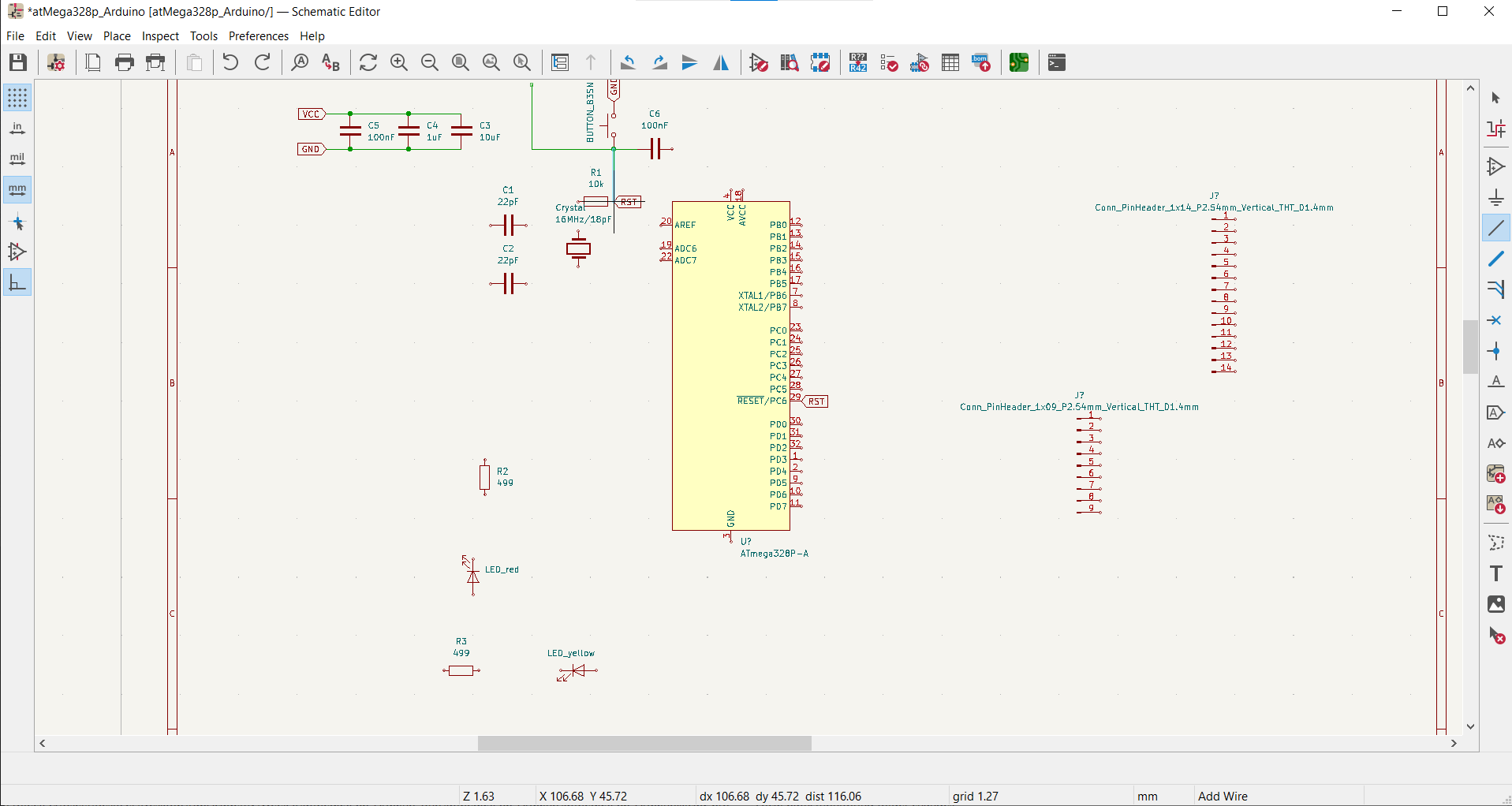
I laid the components out roughly where they should go and then started creating my logical connections using the Add a Wire tool.
Tags
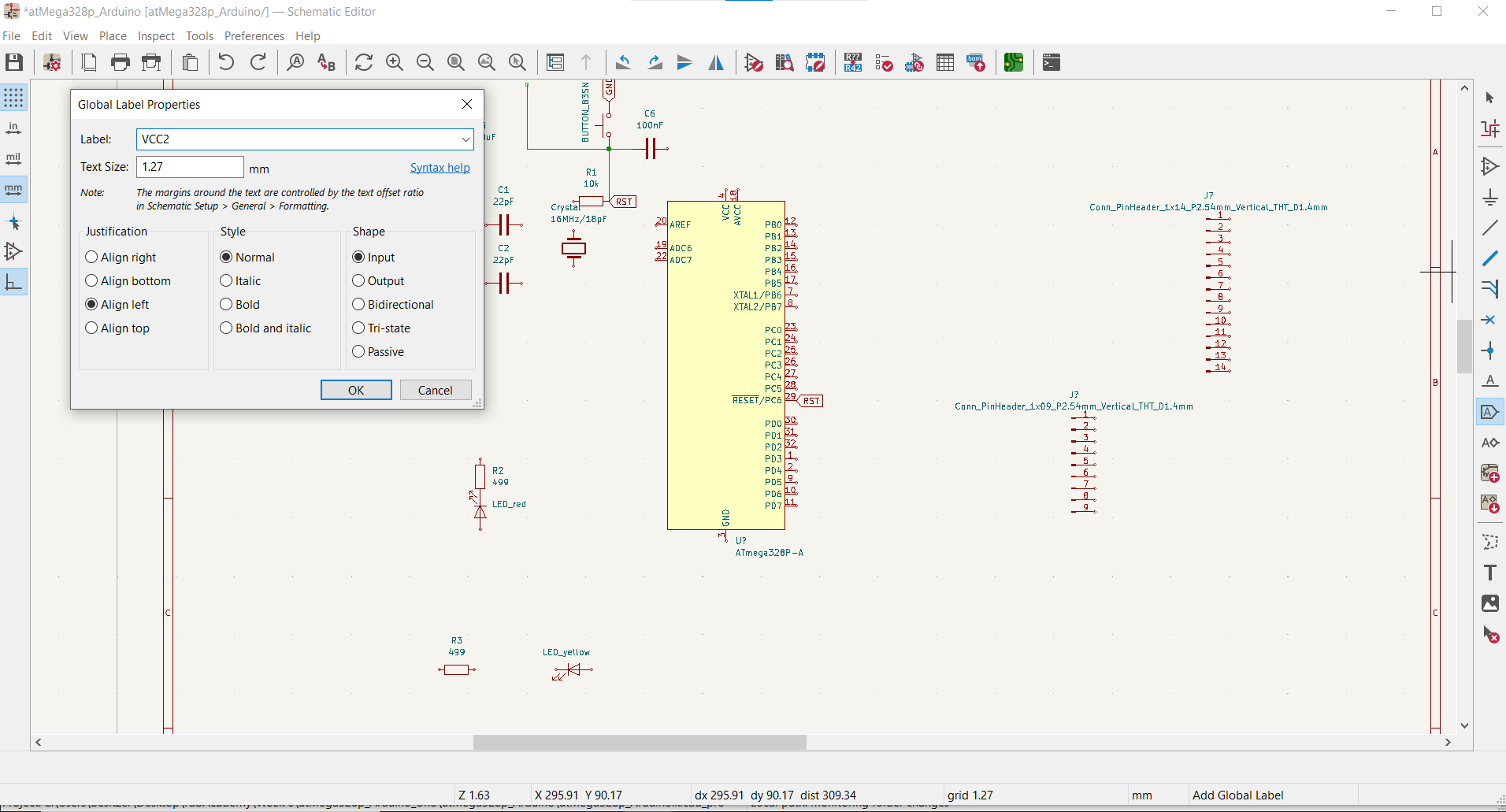
I wanted to be careful to not make the schematic so busy that I couldn't read it anymore, so I also employed a lot of tags using the Add a Global Label tool. This is very convenient for keeping the number of wires down on complex boards.
Moving On
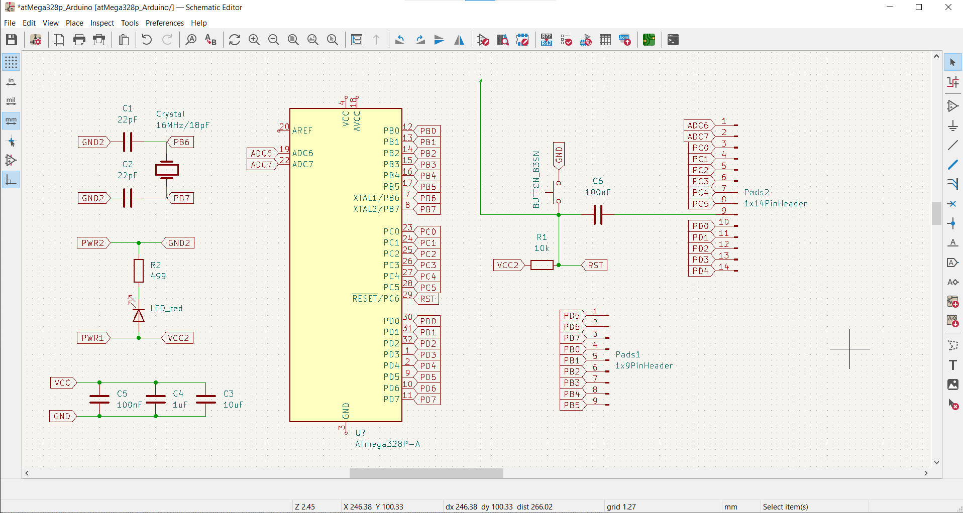
There were a couple things I didn't really understand from the original schematic, but eventually, I had it more or less copied and I was ready to add my new button and LEDs to the design.
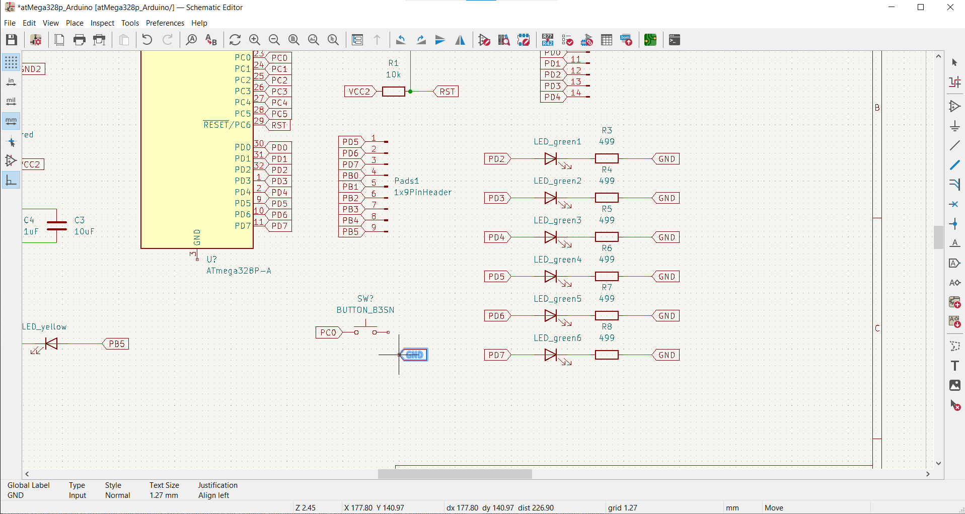
Green LEDs
So next I added the LEDs. The board already sported a red and yellow LED, so I decided to go with green for the new ones to keep everything simple.
Resistors
And of course, I added a resistor in line with each of the LEDs to prevent current from damaging the microcontroller or blowing up the LED.
Pinout
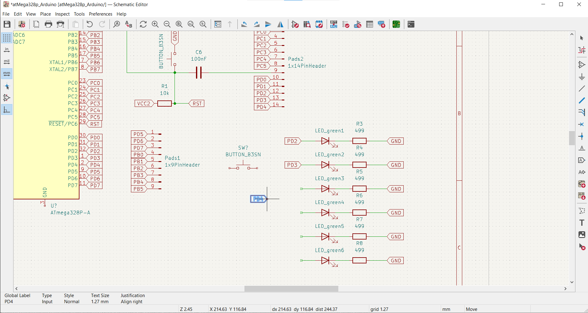
I put the six pairs of LEDs and resistors on different digital pins...
And Button
...and I put the button on an analog pin.
Done-ish
Finally, the schematic was complete enough to move on to the blueprint.
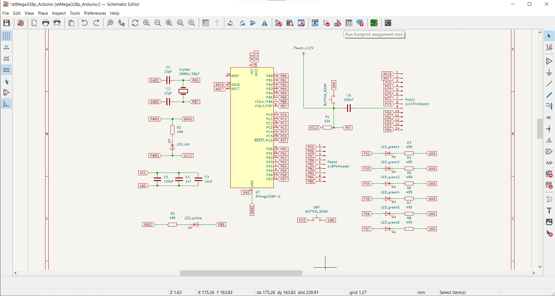
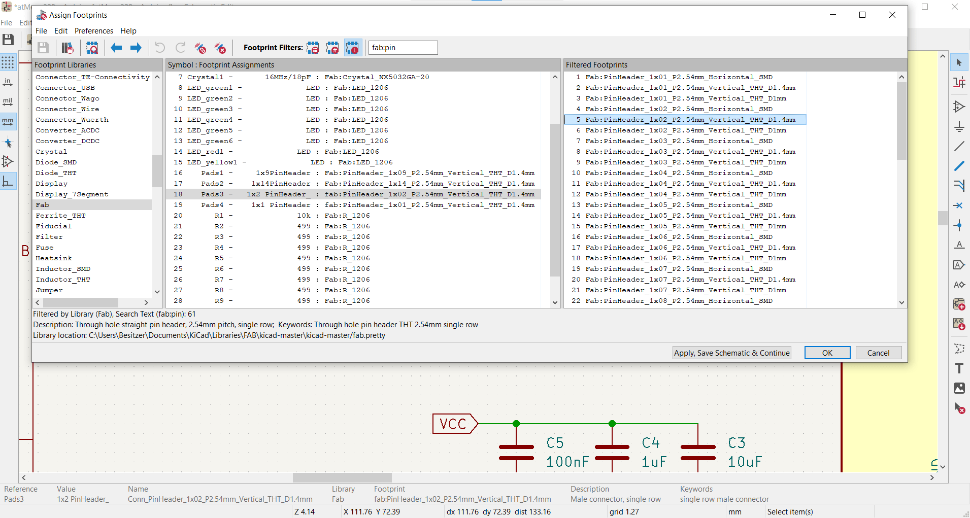
Adding Footprints
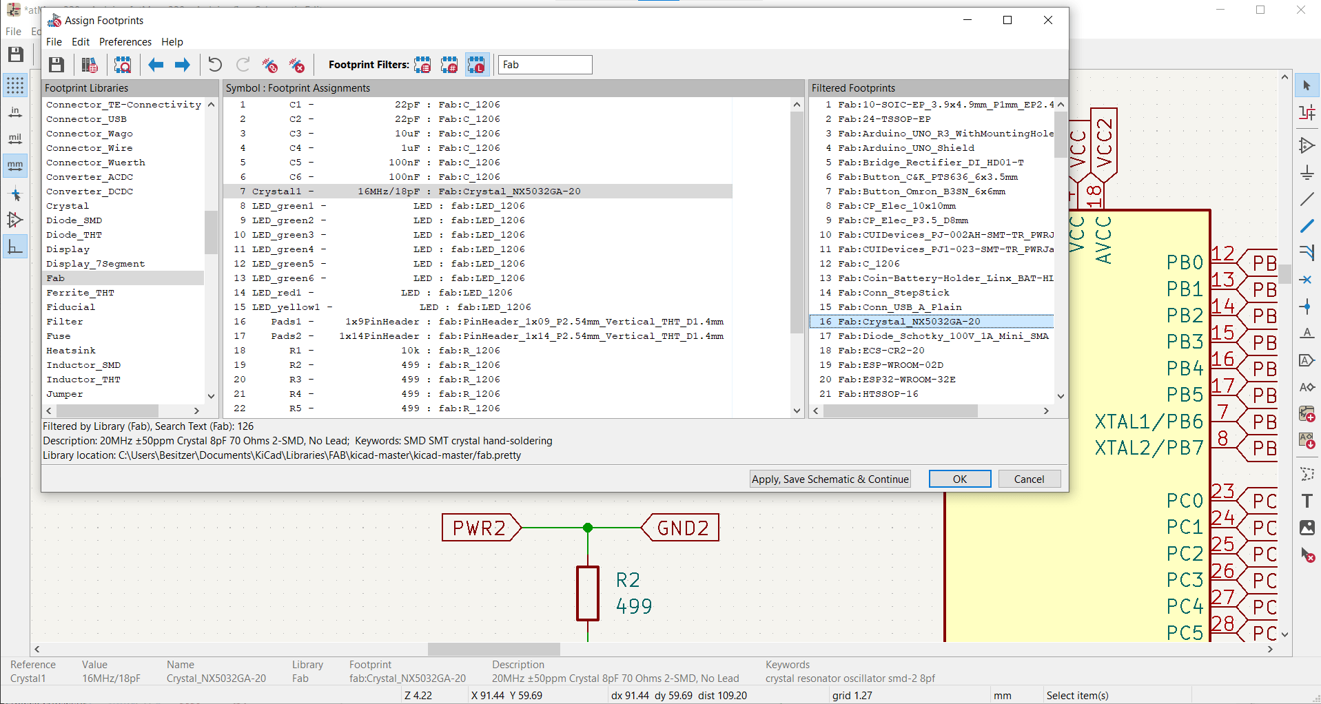
In the Run Footprint Assignment tool, I chose the proper footprint for all of the components. Apparently, there is no footprint for the ATmega328P so I had to use the footprint from the Microchip library, once again, after stopping off to double check the datasheet to make sure they were the same as the ones we have in the lab.
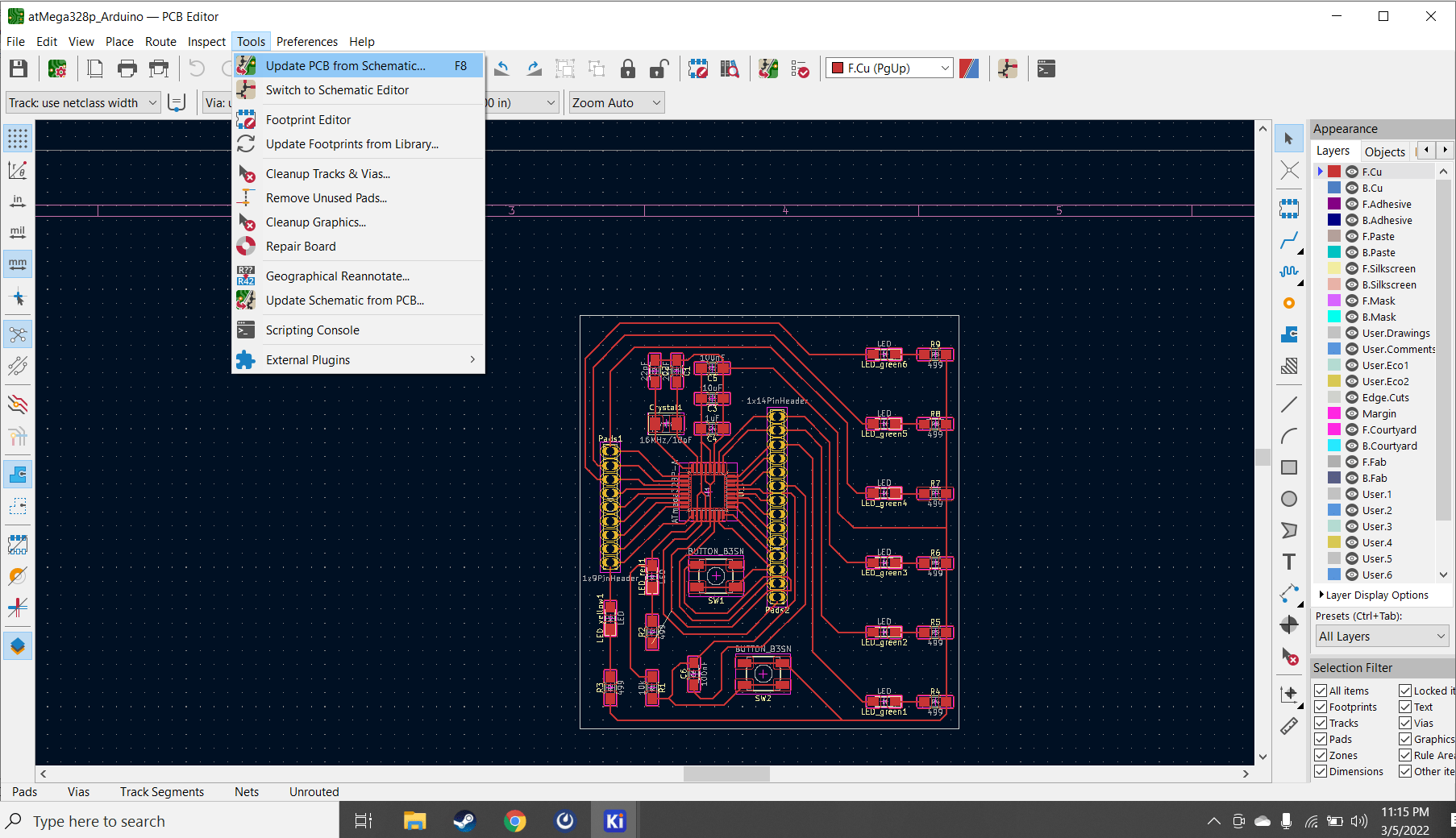
Generating Blueprint
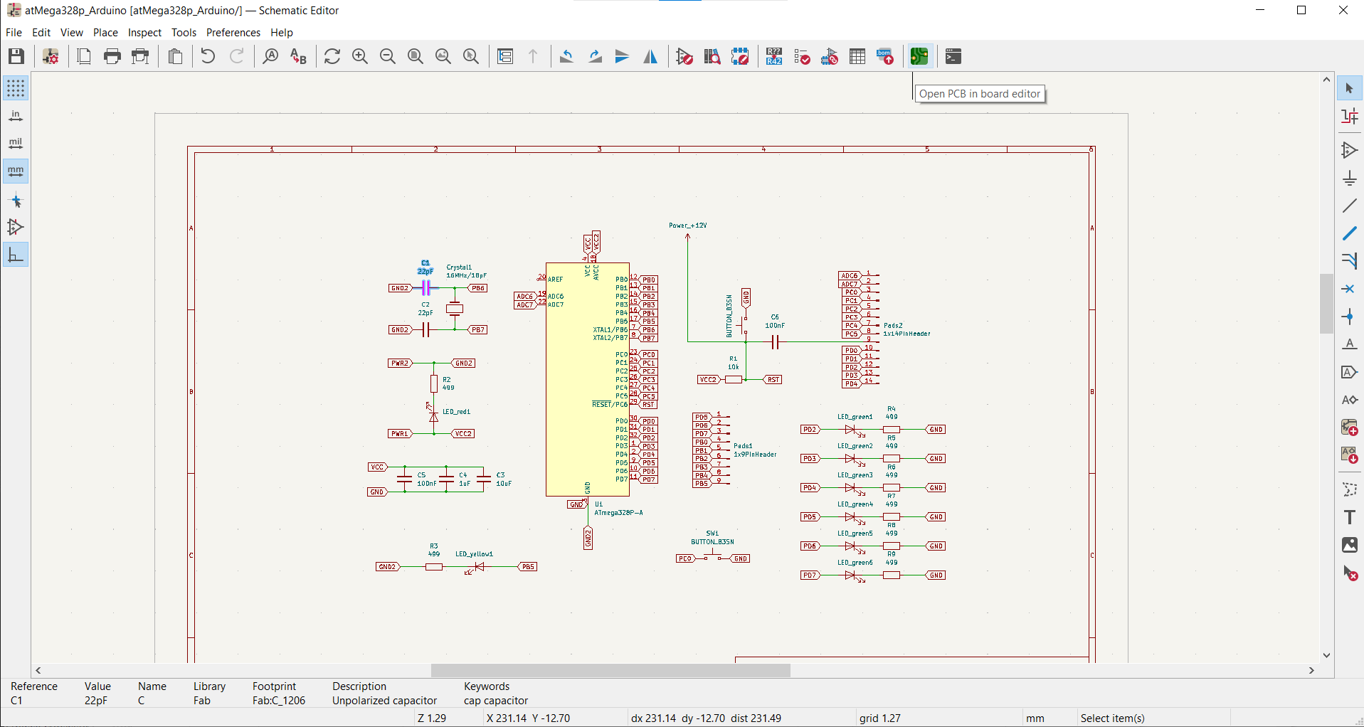
Then I clicked on the Open PCB in Board Editor tool and started my blueprint.
Making the Blueprint
Adding Footprints
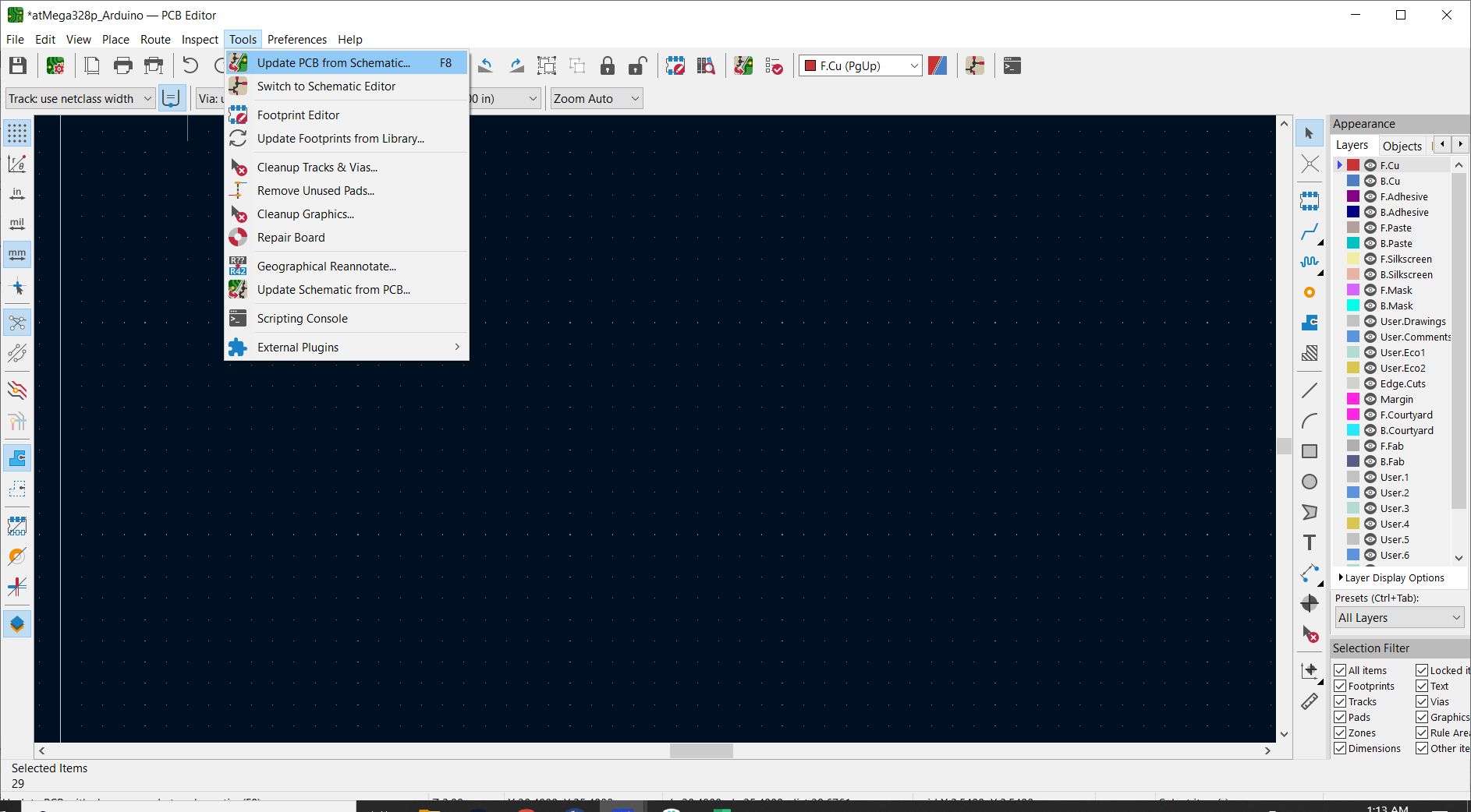
In the tool menu, I clicked on Update PCB from Schematic to bring in all of the footprints of my components.
Errors:0, Warnings:0
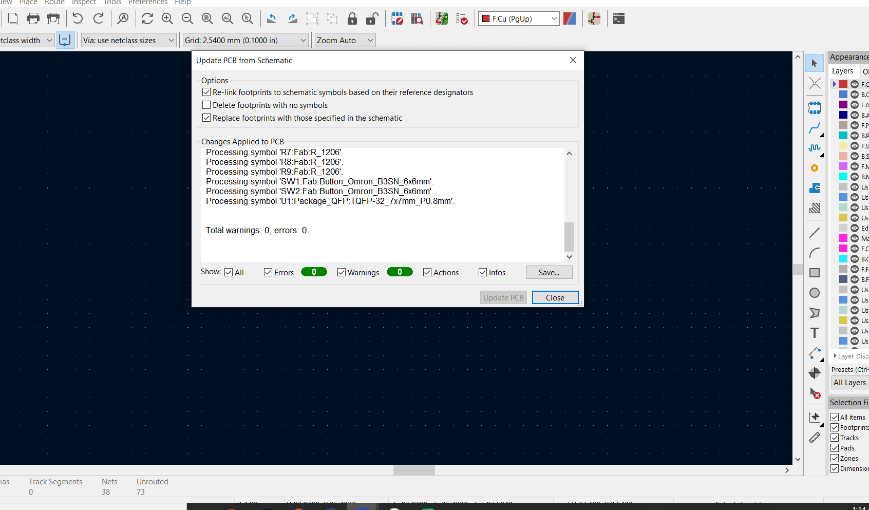
I was happy to see zero errors and warnings in the dialog box indicating that I had correctly assigned the footprints (not a guarantee, but evidence lol).
Auto-Place
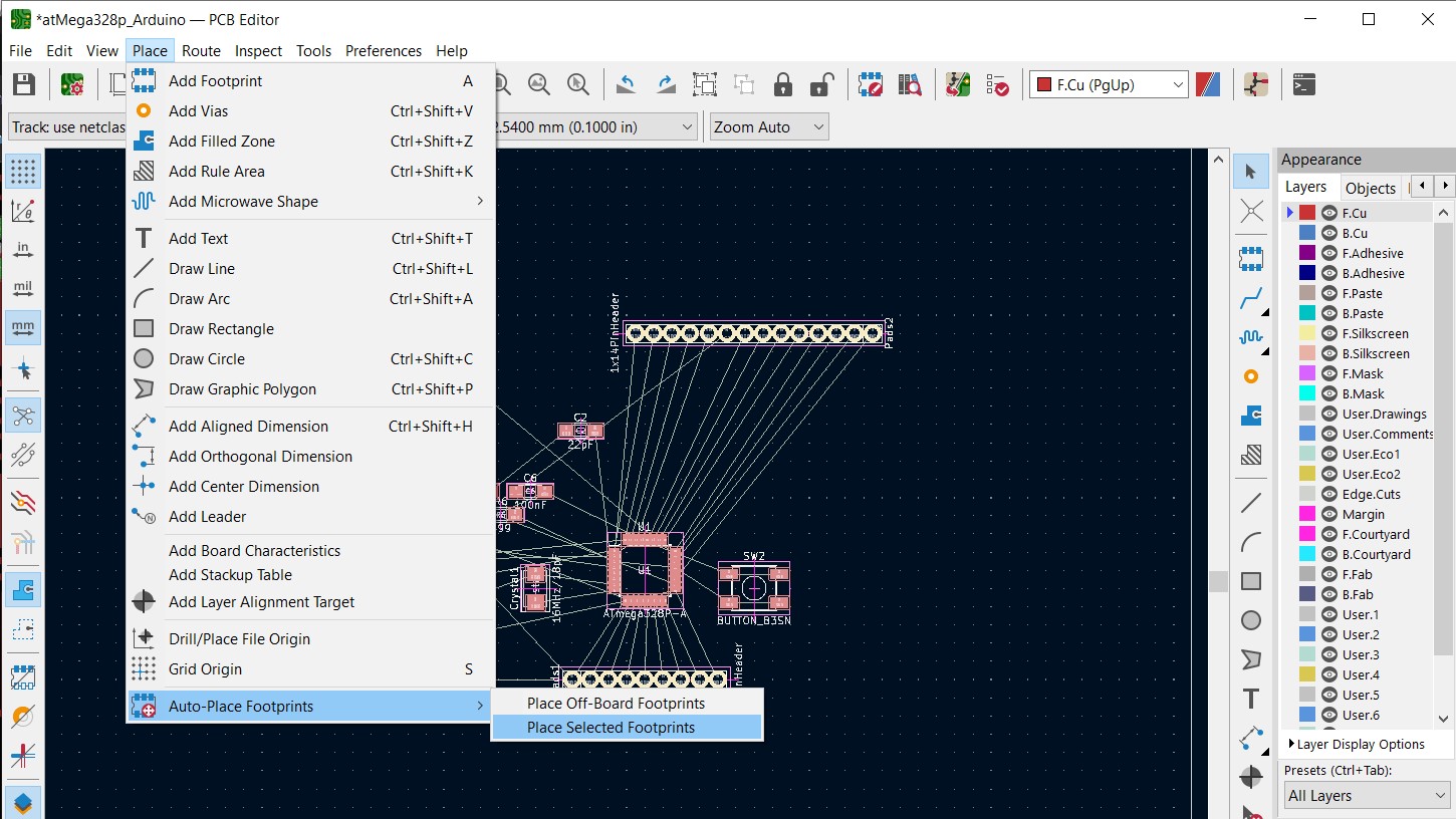
I tried to use the Auto-Place Footprints tool from the Place menu, but it just took a long time and didn't really give me anything that made sense so I ignored it and just moved things around by hand for a while until I was satisfied that I would be able to connect the necessary traces.
Route Tracks
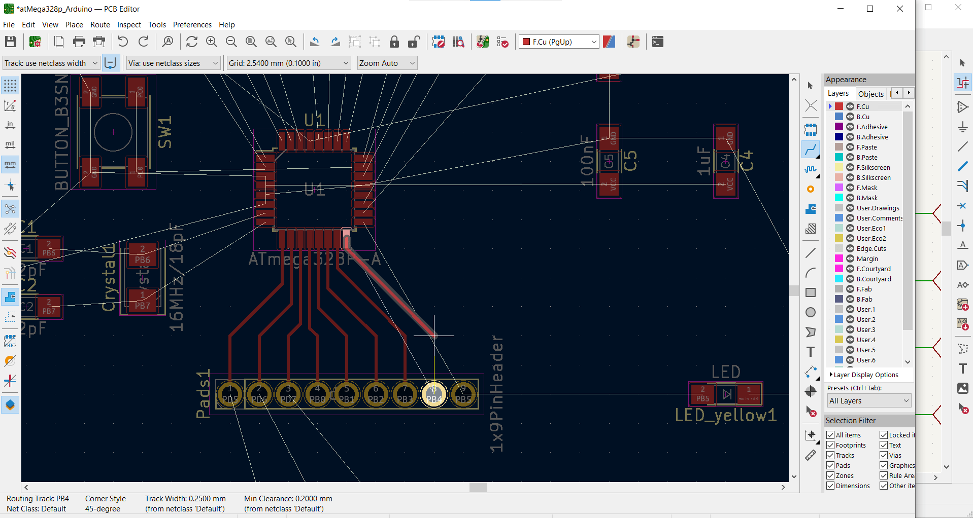
Then I started laying down those traces using the Route Tracks tool.
Oval Pads
I also changed the round default pads, to oval shaped pads as we were shown by Ahmed. This gives a little better surface for soldering and a more robust connection at the pinheaders.
Original Replicated
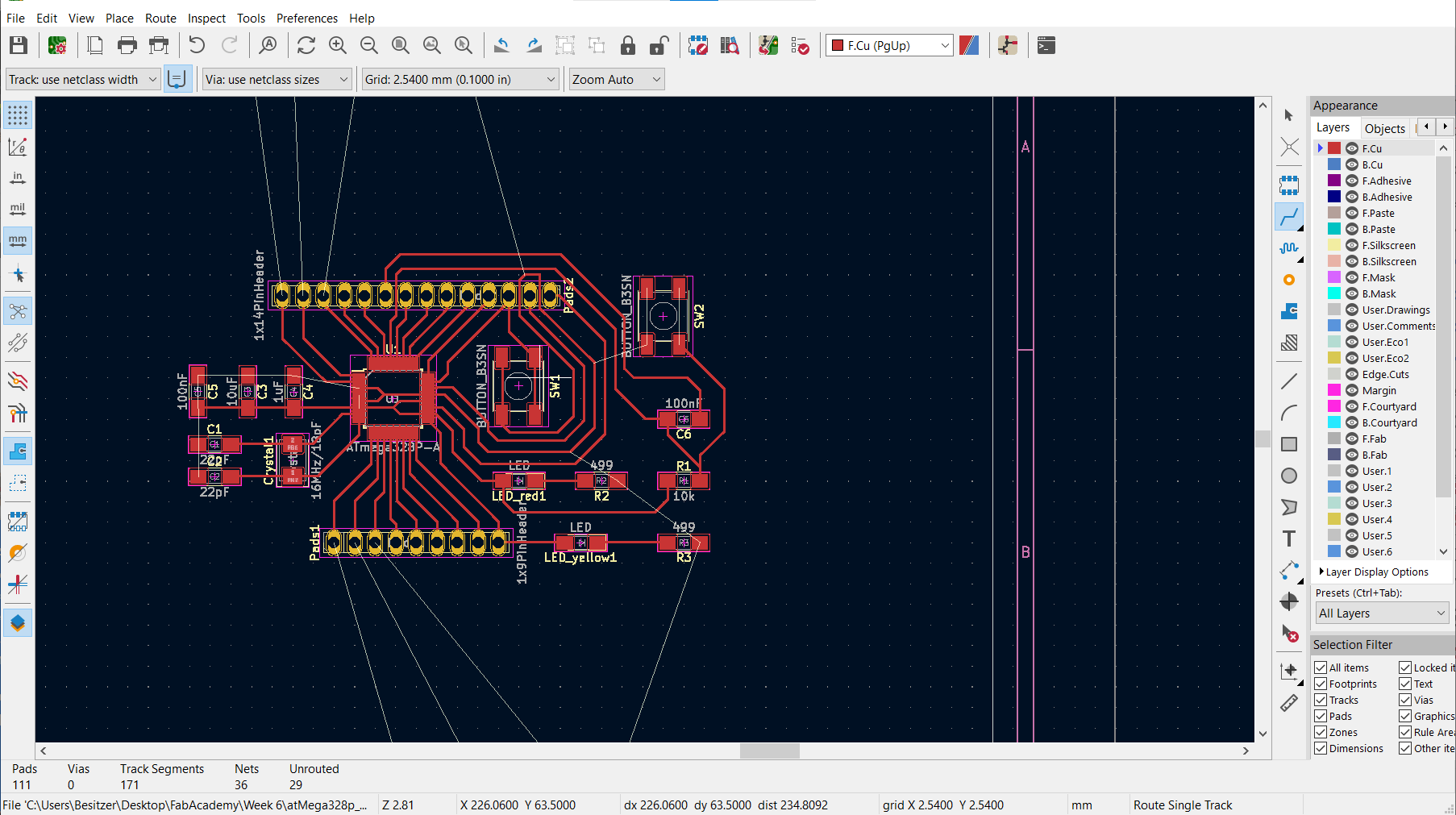
It took some time, but eventually I had the whole original circuit board...
New Components
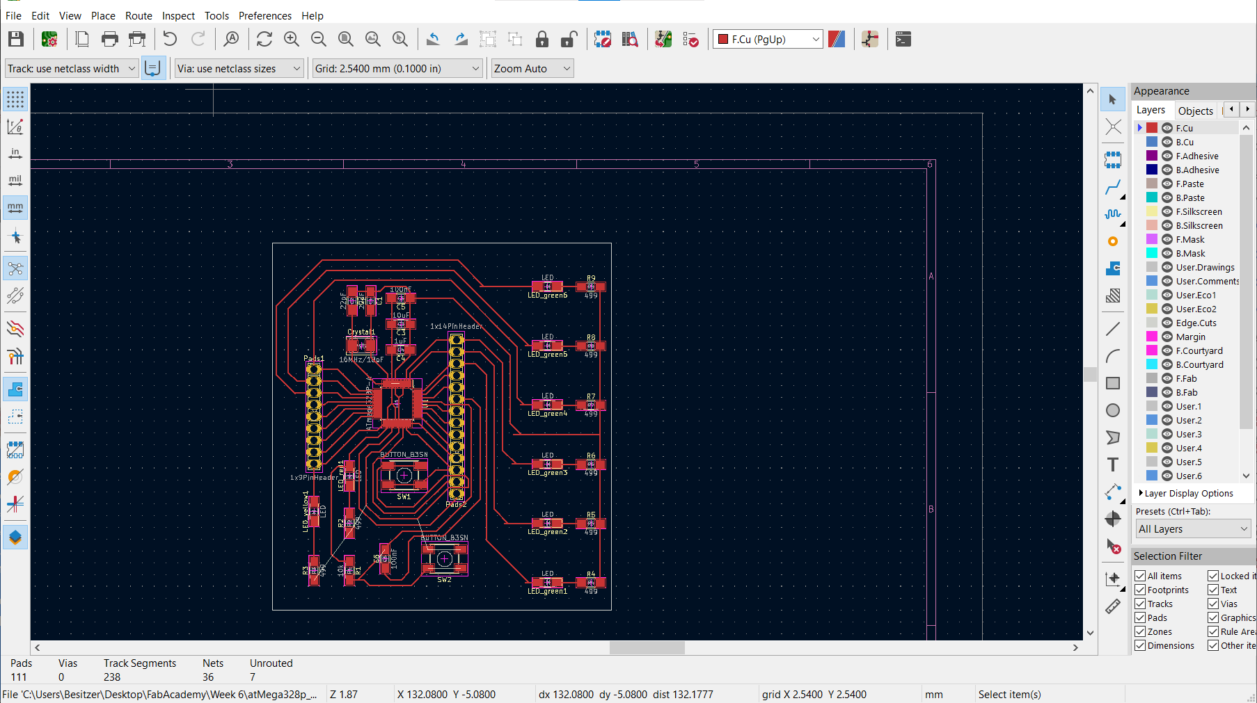
...so I added my new button and LEDs. I wanted it to look nice (and make sense) so I put them in a line on one edge of the board.
Measure Twice
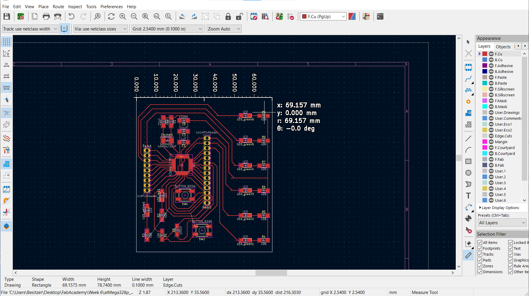
I also regularly used the Measure tool in the Inspect menu to make sure that I stayed within 70 mm for the narrow dimension since that is the size of our PCB blanks in the lab.
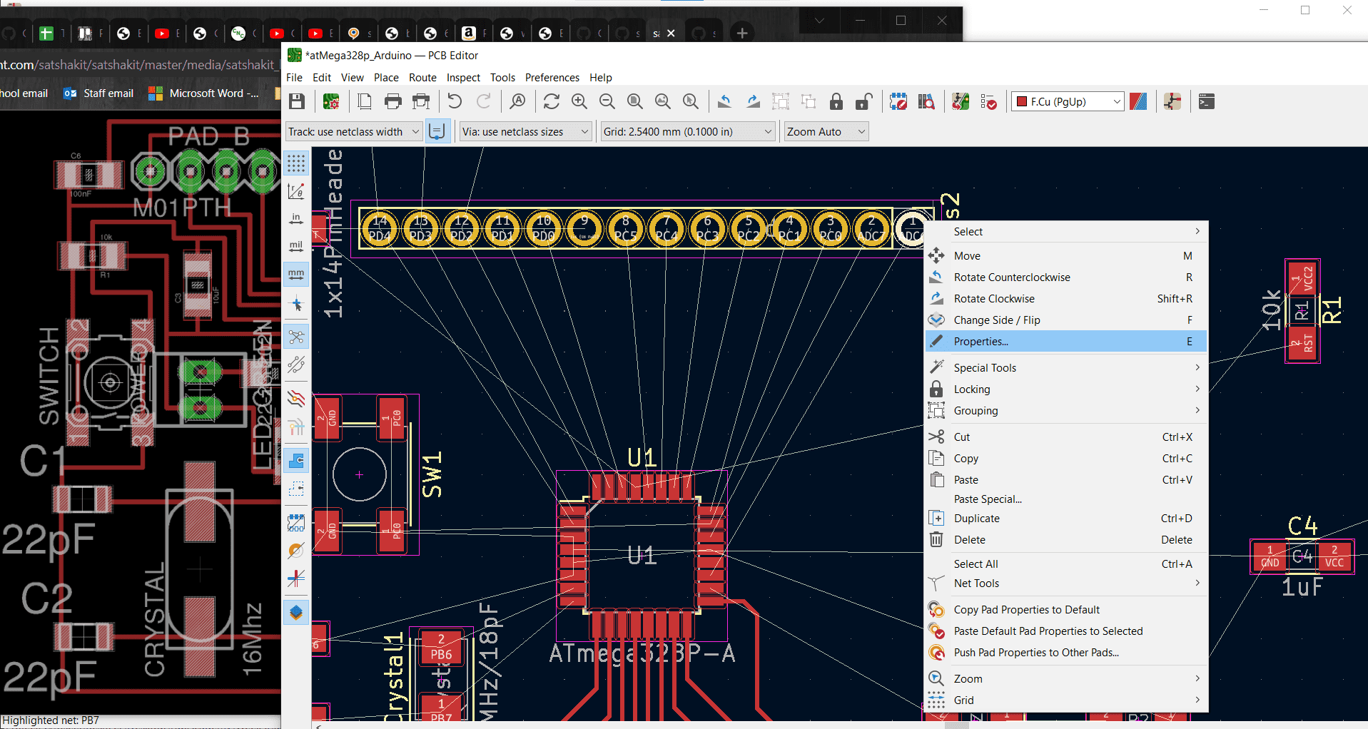
Change Track Width
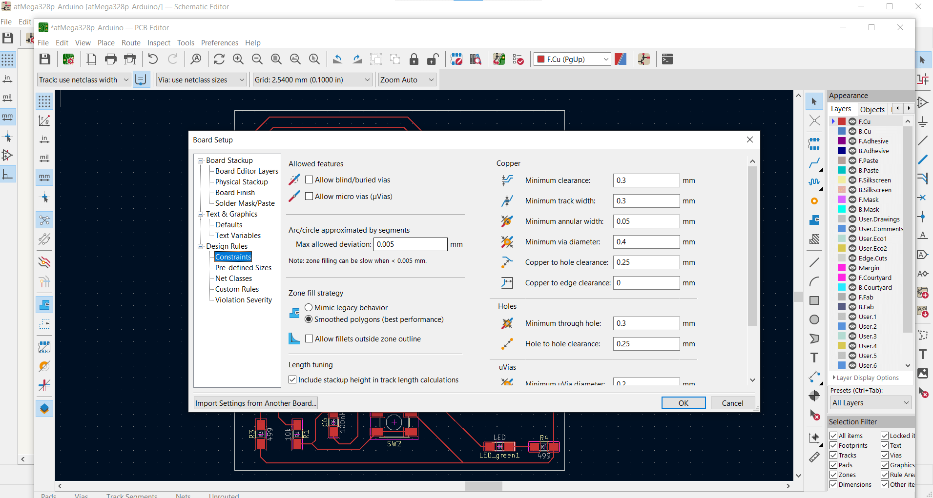
Using a combination of adjusting the Constraints, Pre-Defined Sizes, and Net Classes in the Board Setup and playing around with the Edit Track and Via Properties tool in the Edit menu, I was able to change my track width from the default 0.25 mm to 0.35 mm.
New Pinheaders
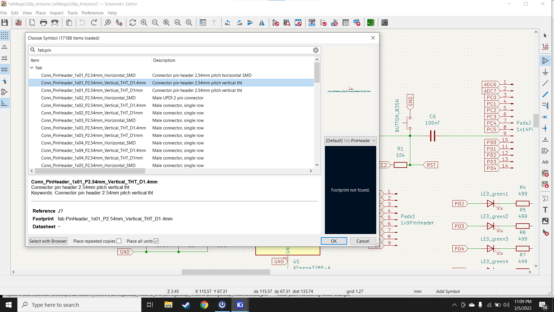
I also needed to deal with the few mystery components and the power inputs. I went to Marcello once more with my questions and he told me to simply replace them with small pinheaders...
Added to Schematic
...so I went back to the schematic and added them...
And to Blueprint
...and then added them to the PCB...
Footprint
...after assigning the new headers a Fab footprint, of course.
Final Result
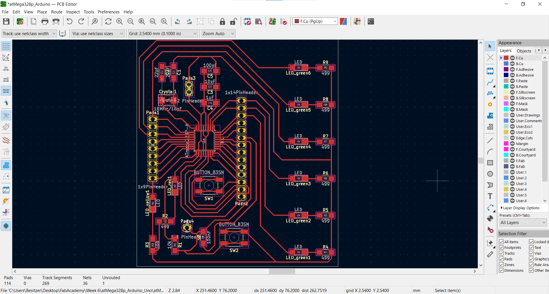
I was lucky that I only had to rearrange very slightly to accommodate the new pinheaders in the blueprint. In the end, everything fit and I was ready to make some gcode.
Missed a Spot
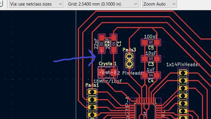
The observant among you might notice that I forgot to add a trace here. This mistake would haunt me later.
Generating G-code
Export SVG
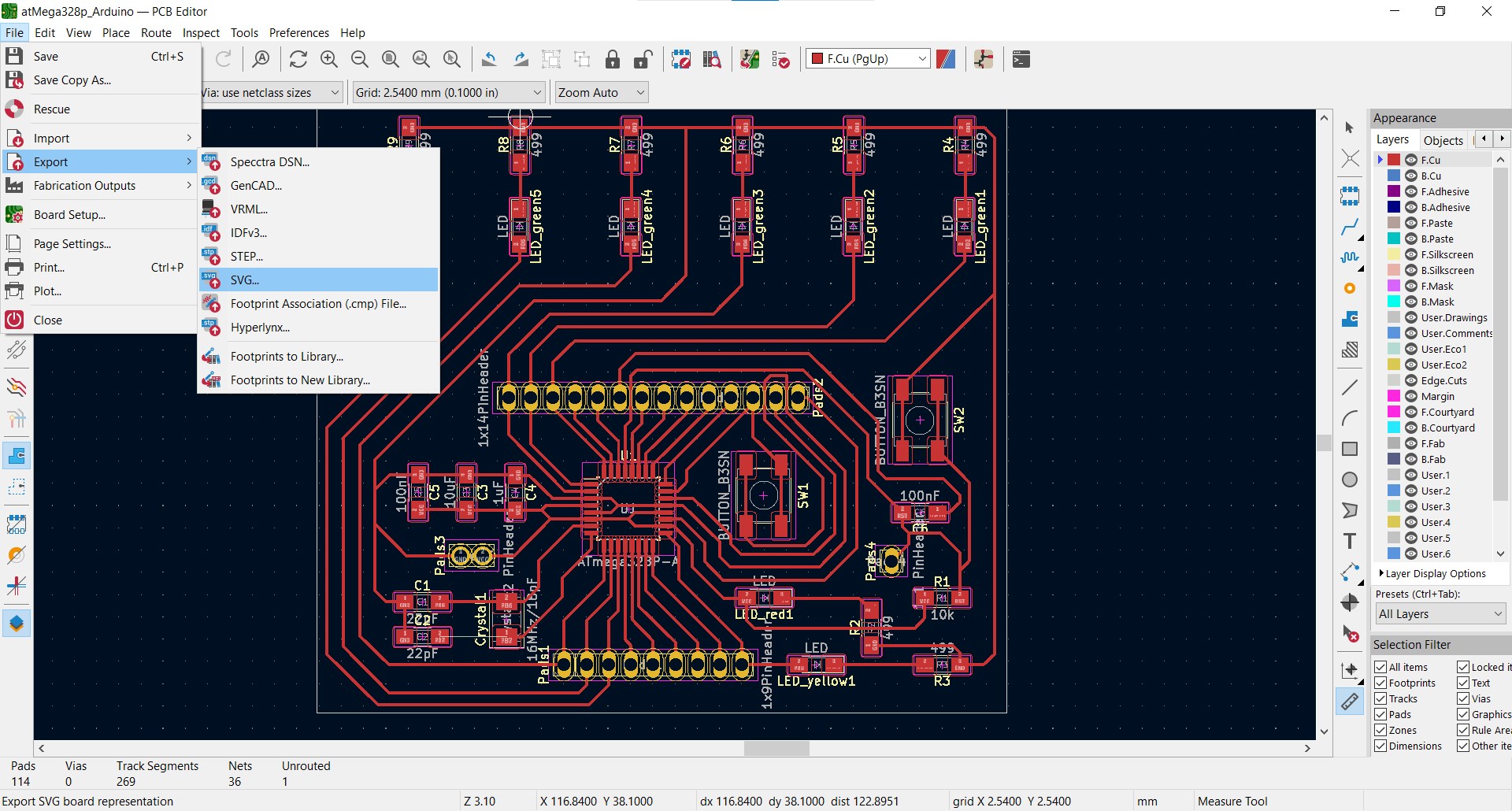
I began by exporting a black and white SVG file from KiCad using the File menu. This would allow me to open it in Inkscape so I could eventually get the PNGs I needed.
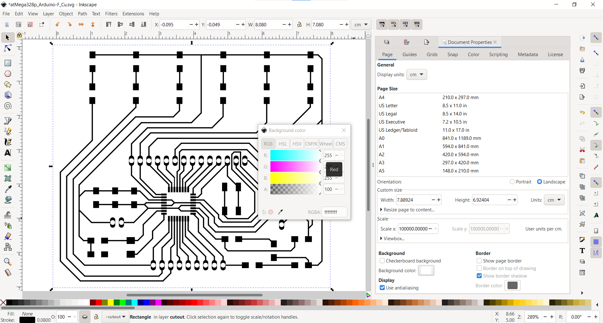
Cutout Rectangle
The first thing I did in Inskape was to add a new rectangle to define my cutout region.
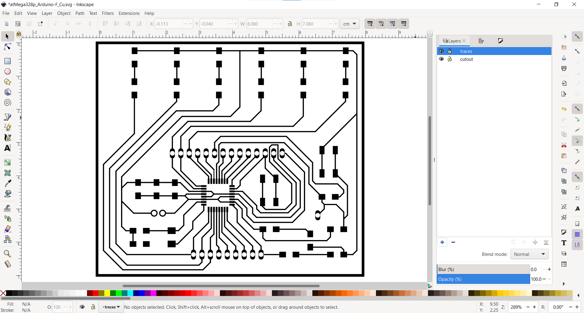
New Layers
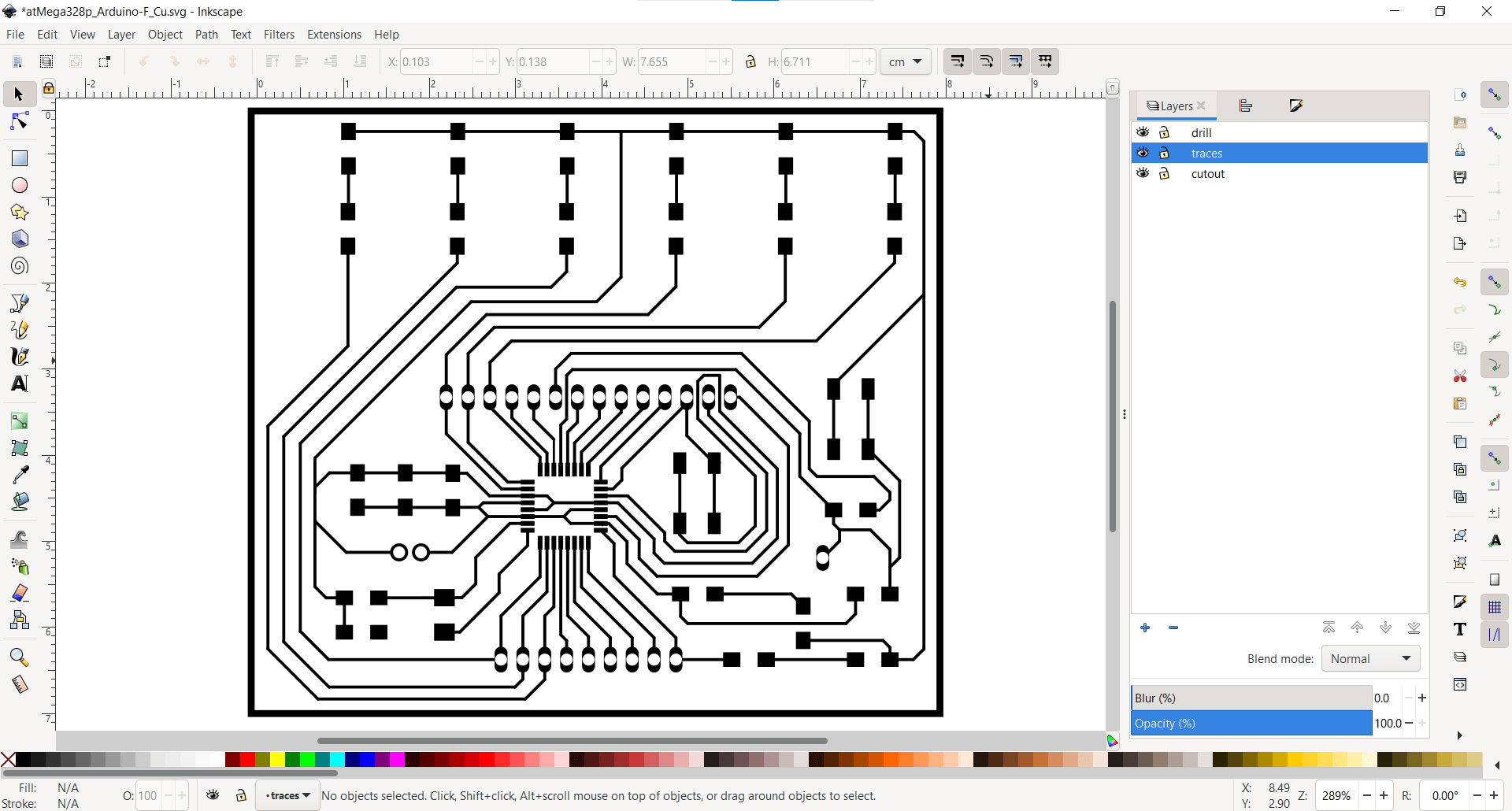
Then I created three new layers in the Layers tab and named them appropriately.
Splitting PCB into Layers
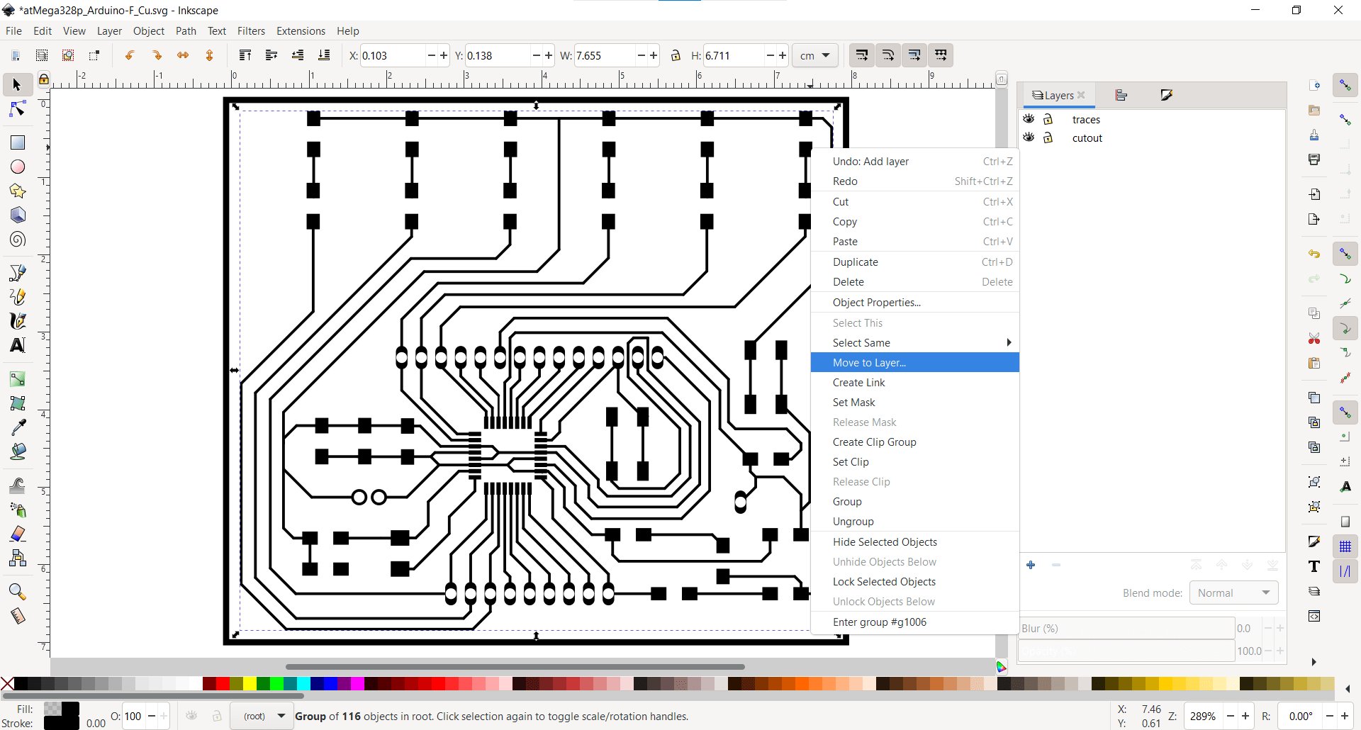
And moved the different parts of the blueprint to their respective layers
Export PNG
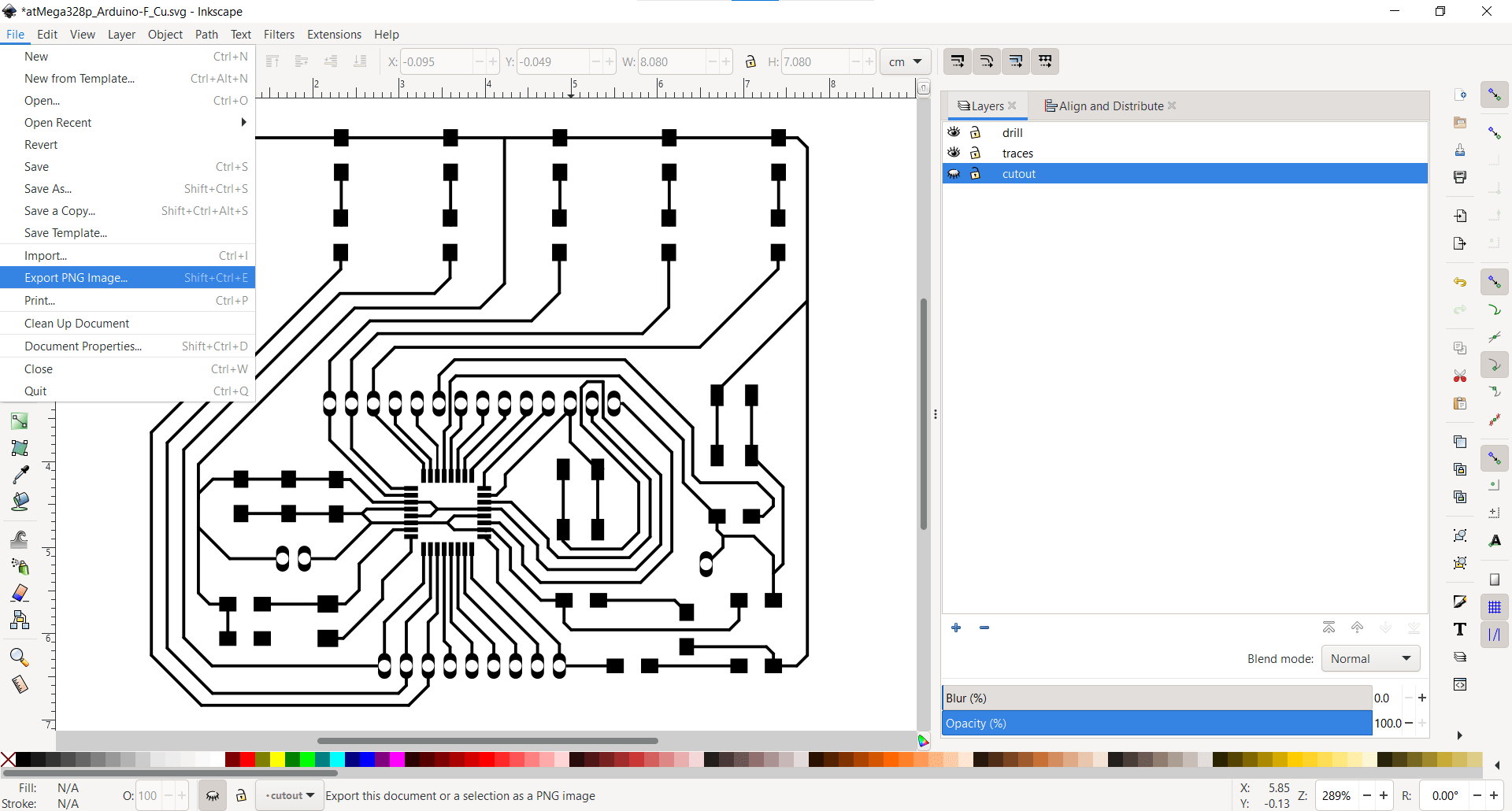
Finally, I was ready to export PNGs for each of my layers (or so I thought).
MODS
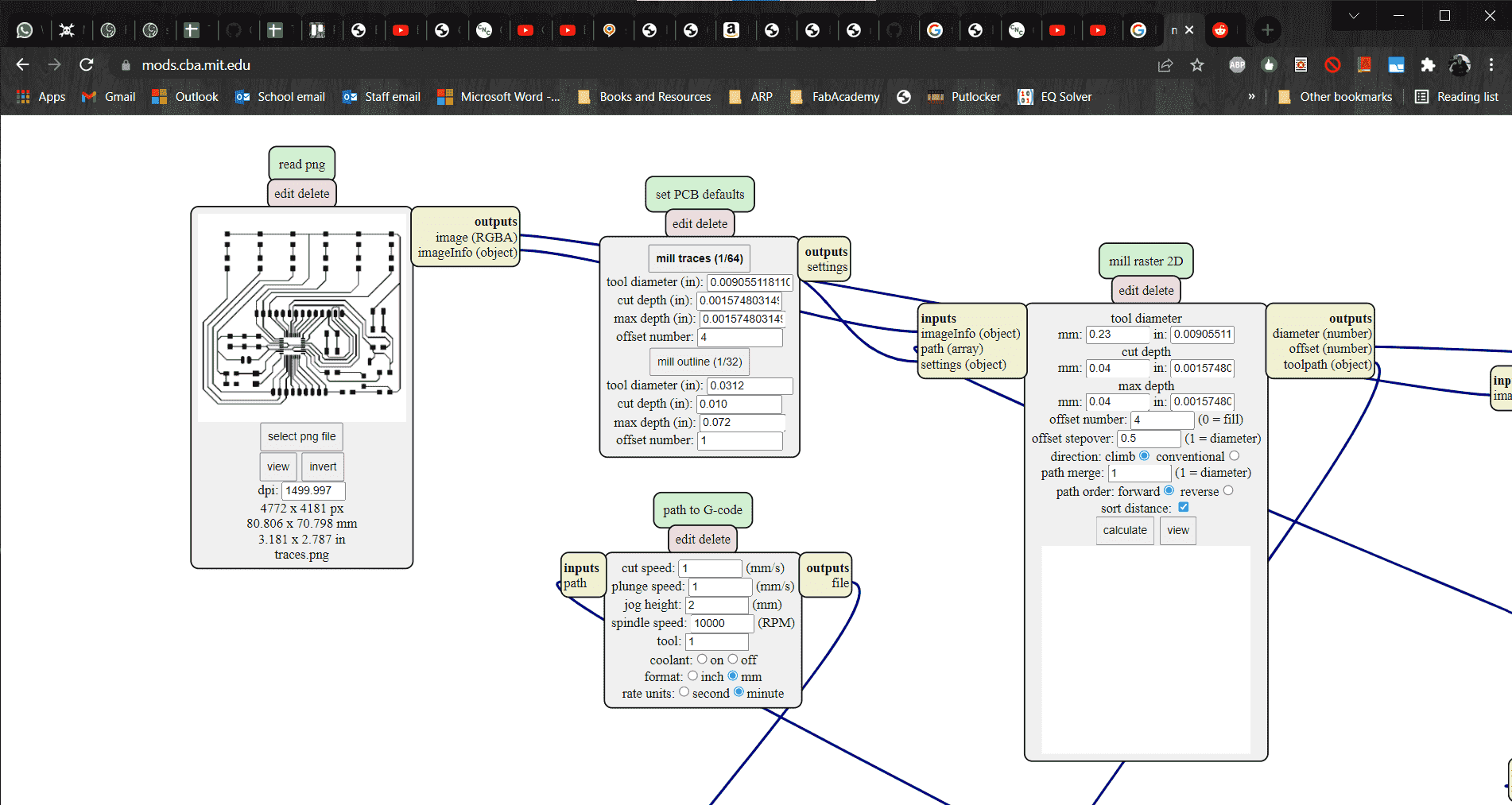
I opened the new PNG up in MODS, but upon clicking the button to invert the image, I realized that Inkscape had exported it with a transparent background instead of white.
Well That's not Right
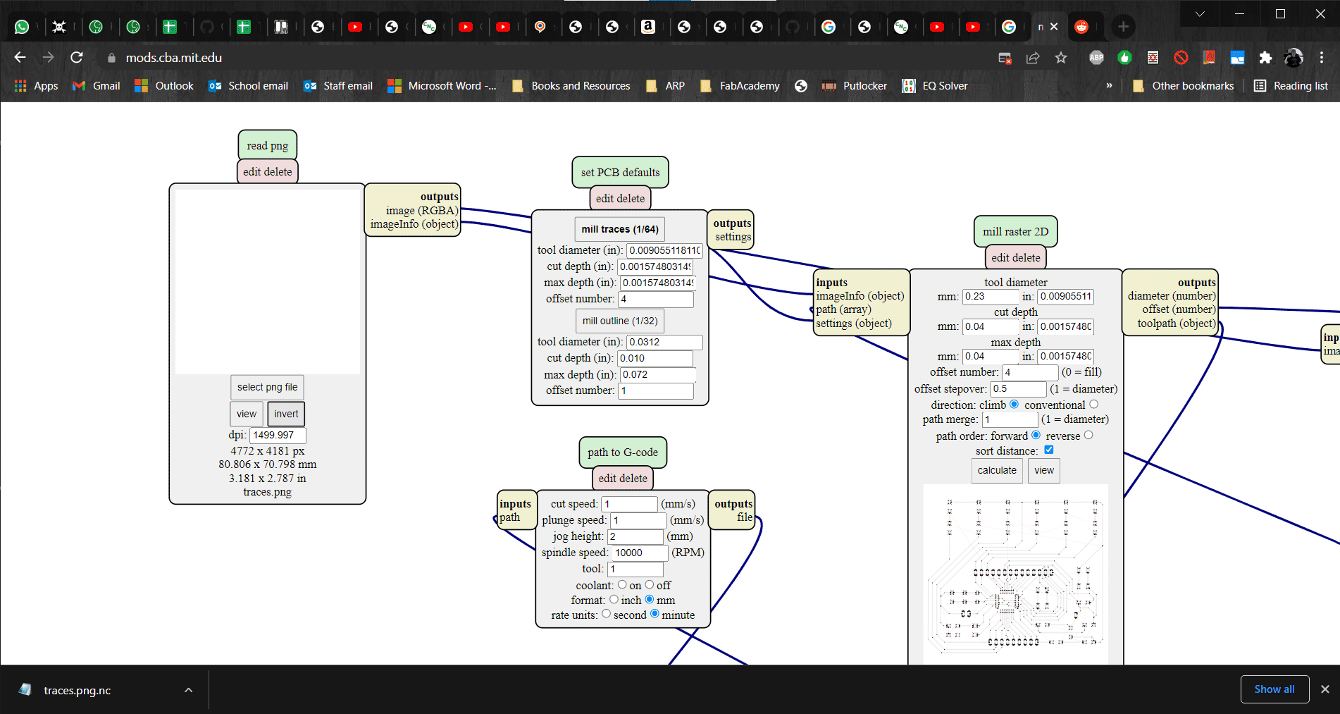
And inverting the image was making it disappear altogether.
Back in Inkscape
So I got back in Inkscape. I had changed the color to white already so I knew I had to be missing something. Eventually, I found this handy guide that explained what I needed to do. Turns out, I had changed the color to white already, but the A-Level (A for alpha) defines the opacity of that chosen color. I set it to 100 and my problem was solved.
Traces and Drills
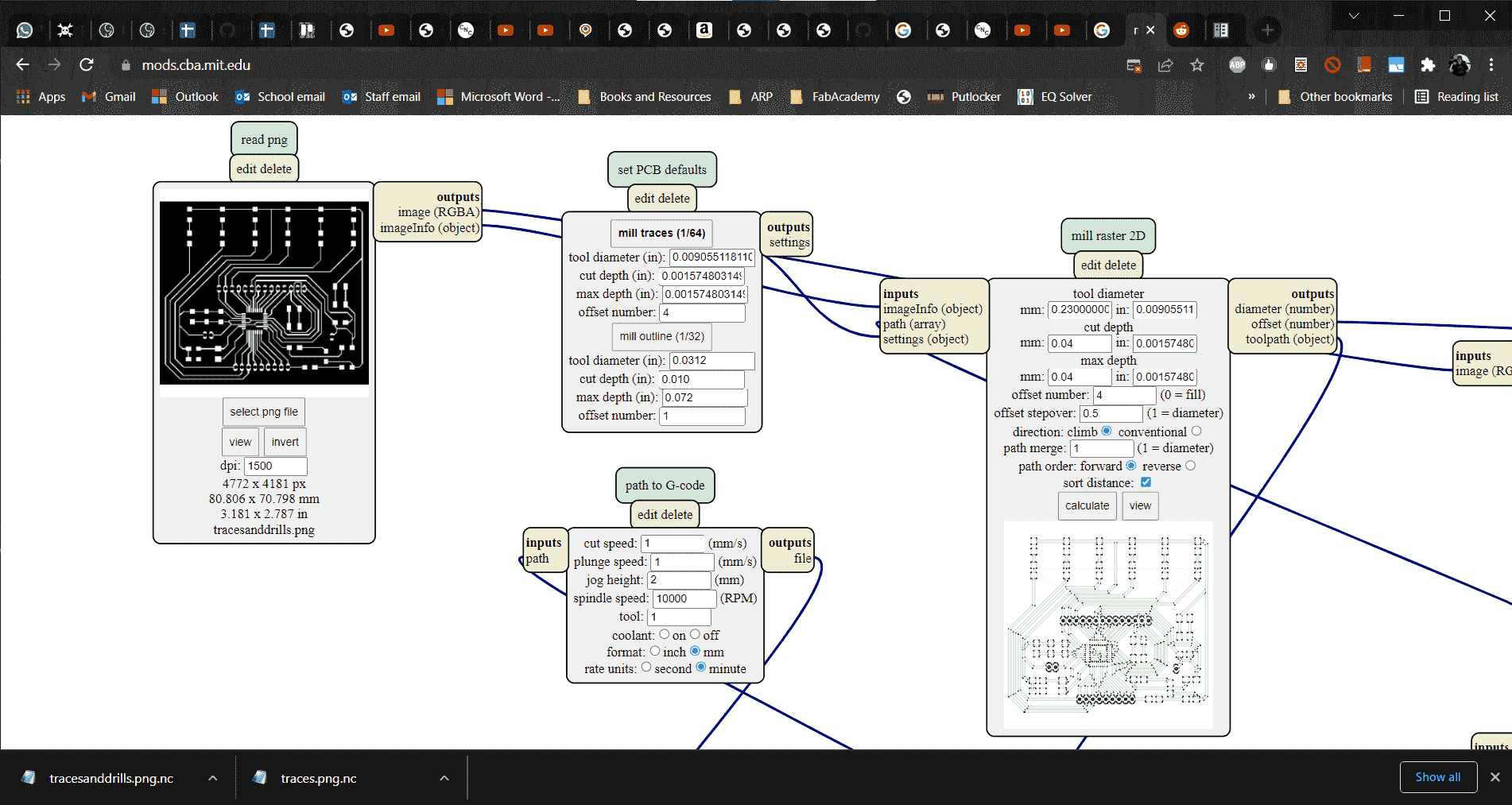
The image was working properly, so I was finally able to use MODS to create the gcode for cutting the PCB on the Genmitsu. I did the traces and drills first using the parameters that I discovered a few weeks ago during the Electronics Production week.
Cutout
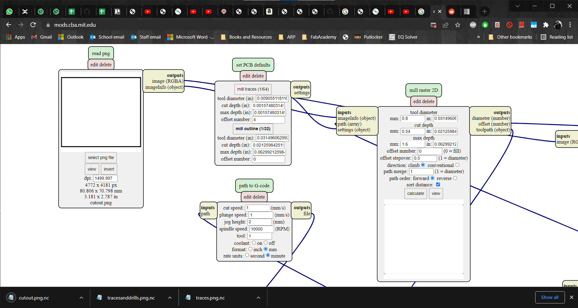
And then I did the same for the cutout.
Cutting the PCB
Back on the 3018 Pro
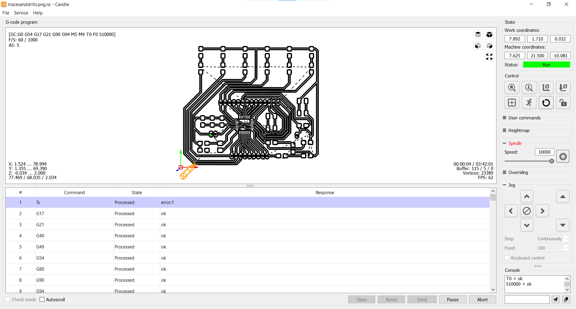
Candle

I opened my new g-code in Candle, but when I tried to send the job to the mill, I was getting an error that I had not seen before.
Problem
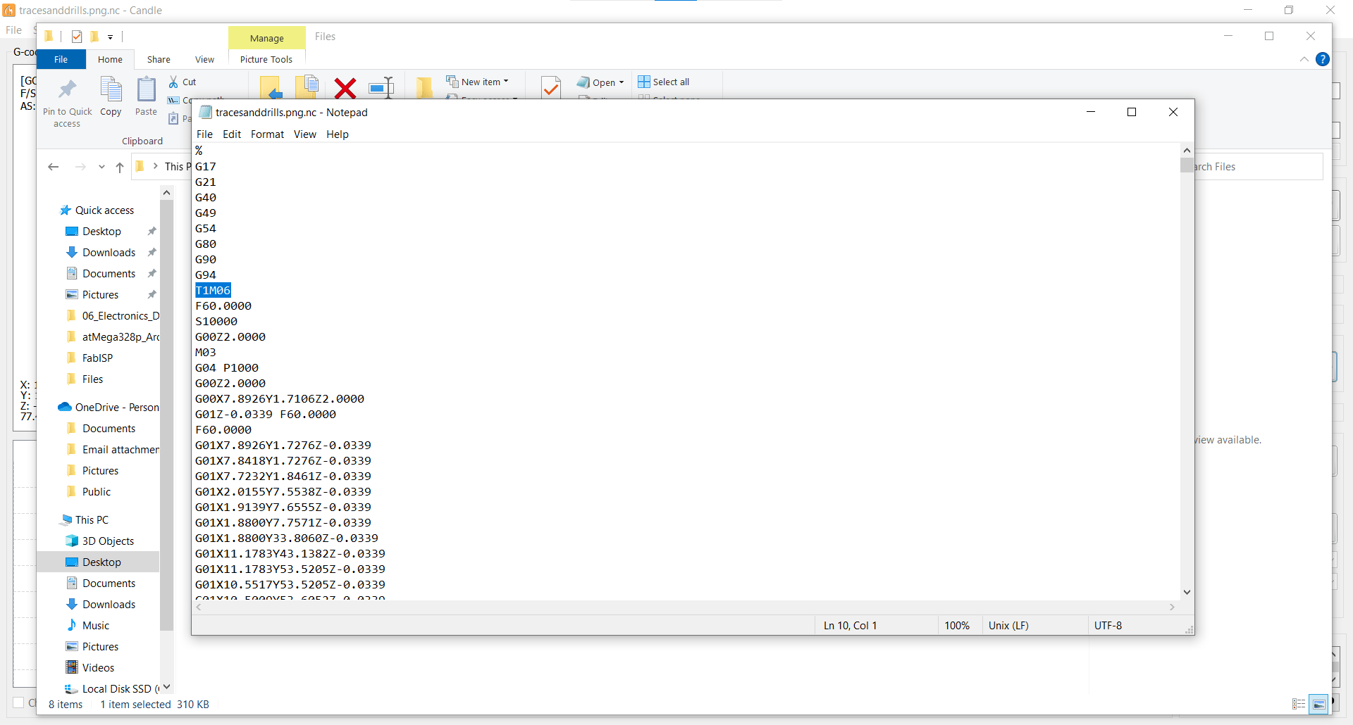
After a bit of troubleshooting, I discovered that I needed to delete this line of g-code that gave the mill instructions about a tool change...
Deleting G-code
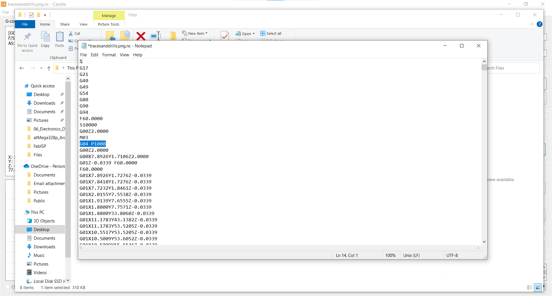
...and this line that tells the machine to pause for one second after not turning on the coolant. I have no idea why these two lines created such a problem, or why I did not encounter it the first few times I used the 3018 Pro, but the solution was easy enough once I discovered the problem.
Job Sent
After that, I was good to go and I started cutting my traces.
Cutout
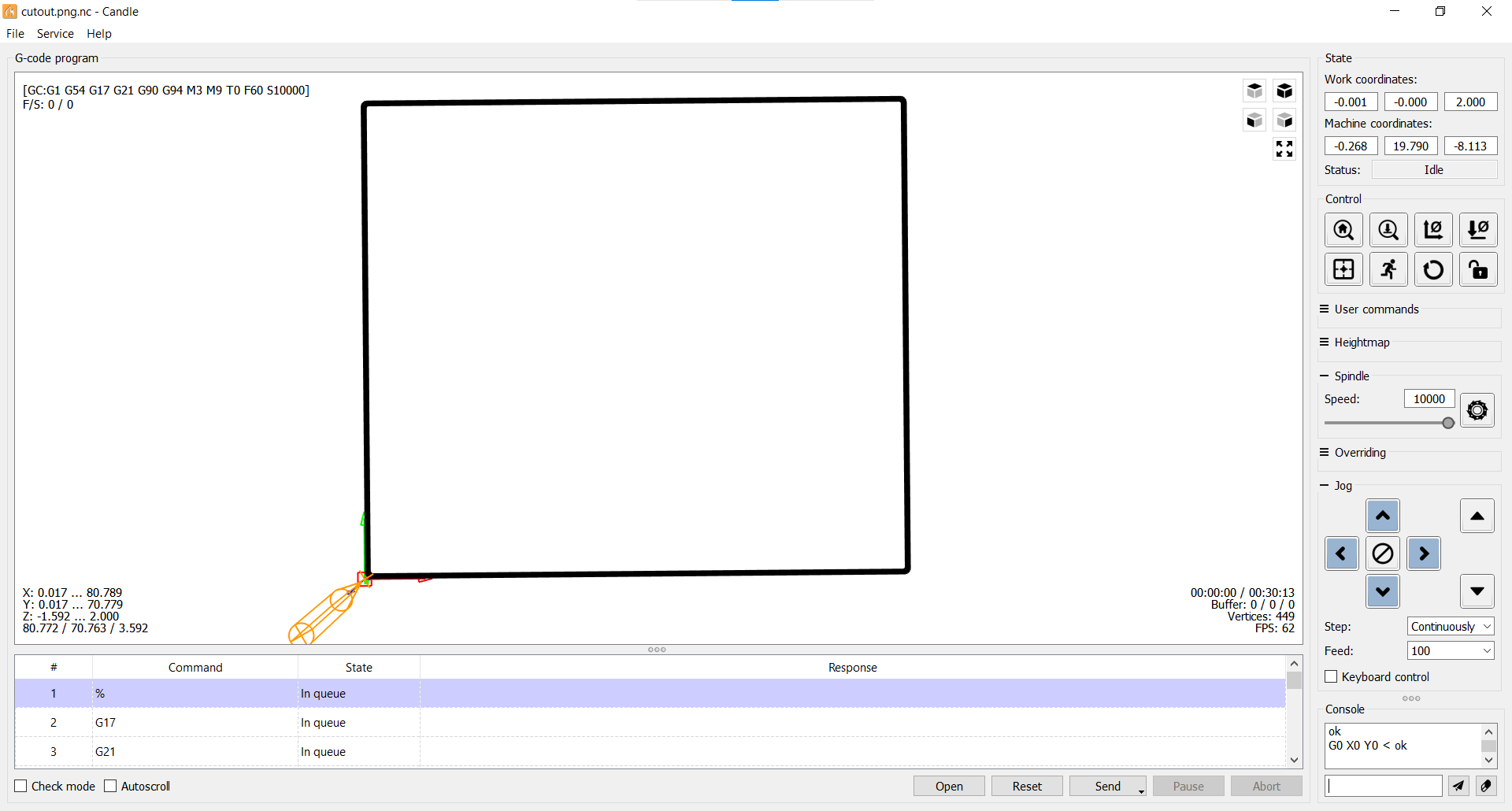
As well as the cutout.
Done
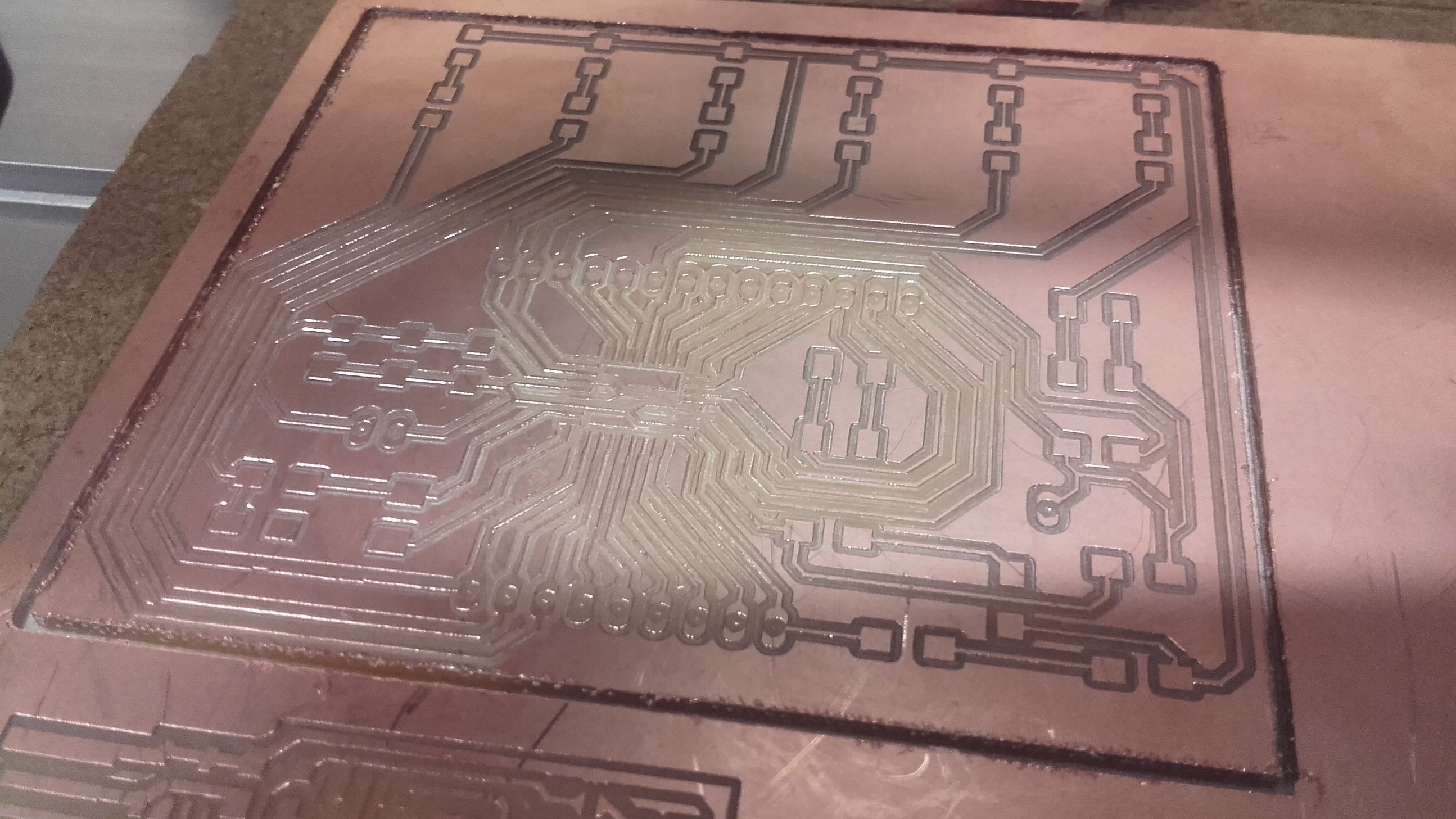
Overall, I am very pleased with the quality that is possible on the Genmitsu mill.
Final Result
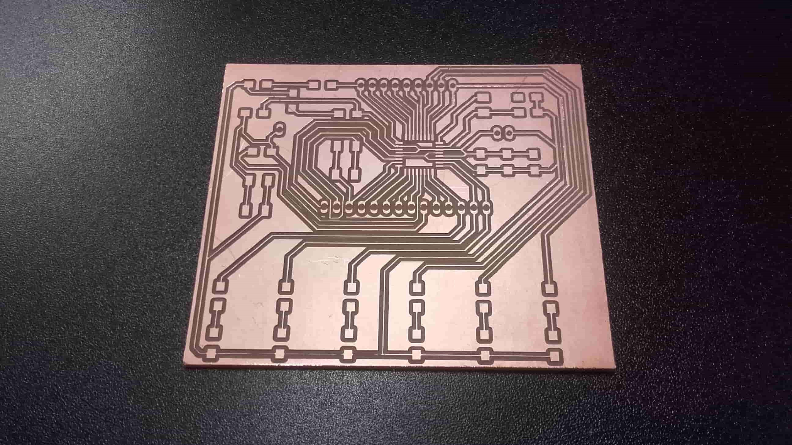
My board isn't perfect, but I'm happy. My results are comparable to what is possible on the much more expensive Roland, at least relative to what has been produced on it in our lab so far.
Populating the Board
Cleaning
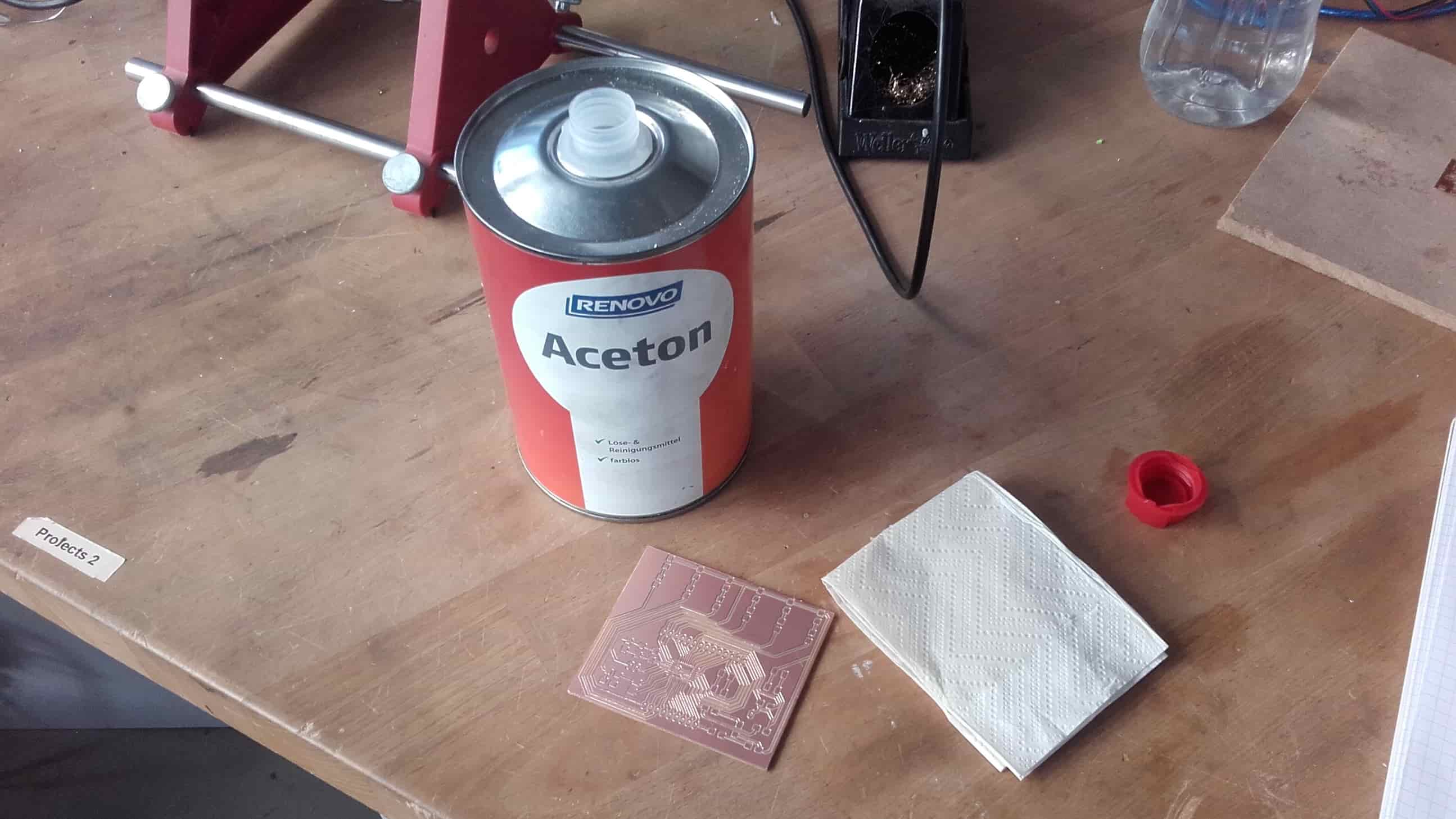
I started by thoroughly cleaning the PCB with acetone.
Collecting Components
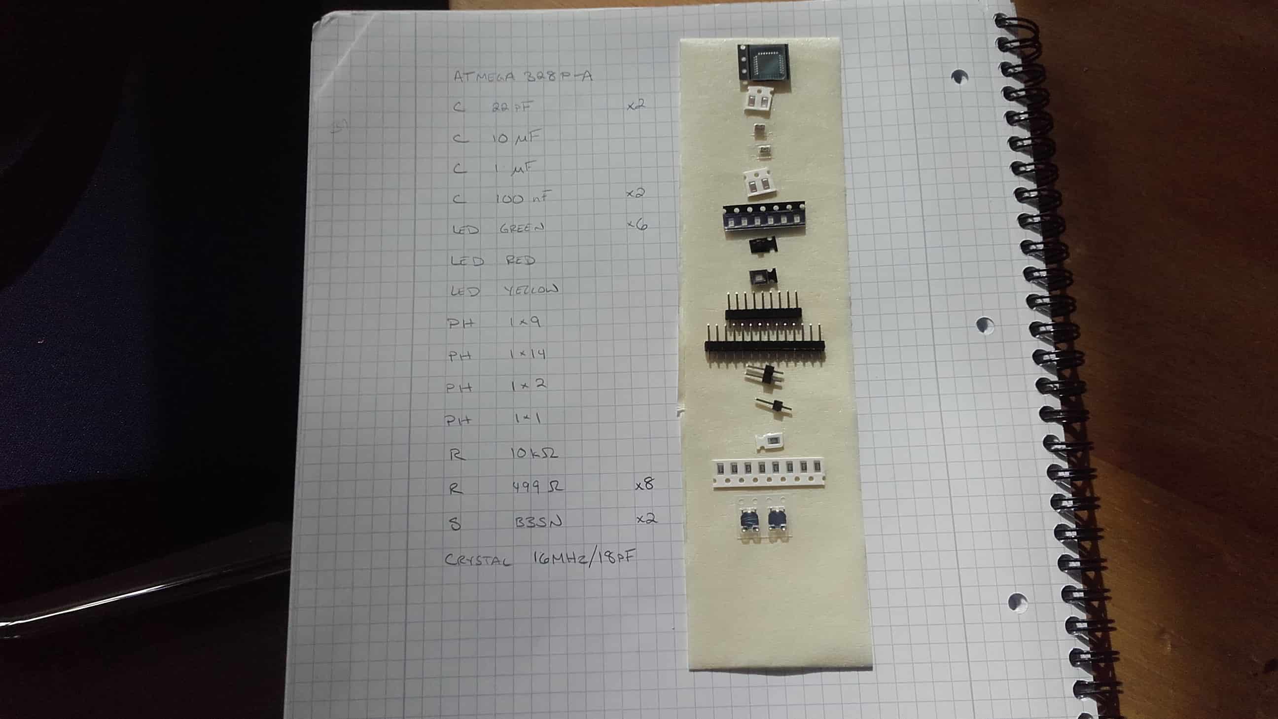
Then, using the method Ahmed showed us a couple weeks ago, I collected all of my components. Unfortunately, we didn't have any 16 MHz crystals that were SMD, so I decided to use one that is 20 MHz. According to the datasheet for the ATmega328P, this is no problem as long as I supply 4.5 - 5.5 volts. Apparently it might cause a problem later with the bootloader, but it can always be replaced if necessary.
Set-Up
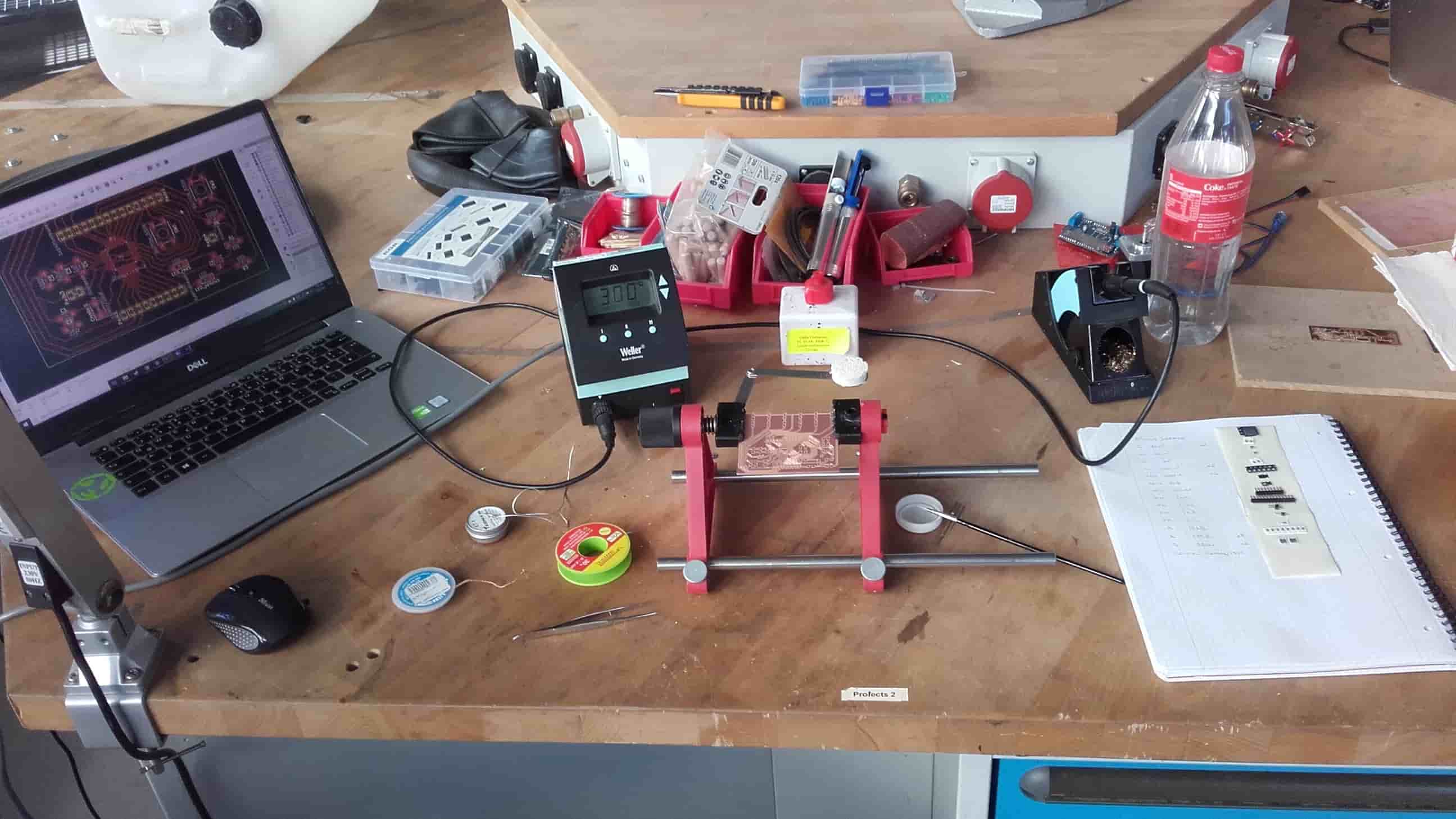
All set up,
Soldering
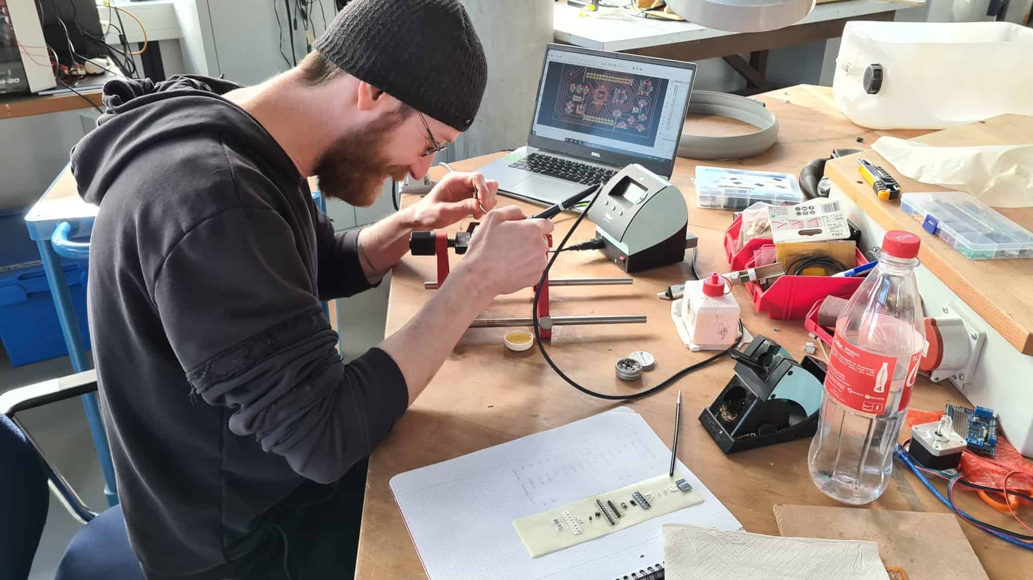
I was ready to begin soldering.
Mistake No. 1
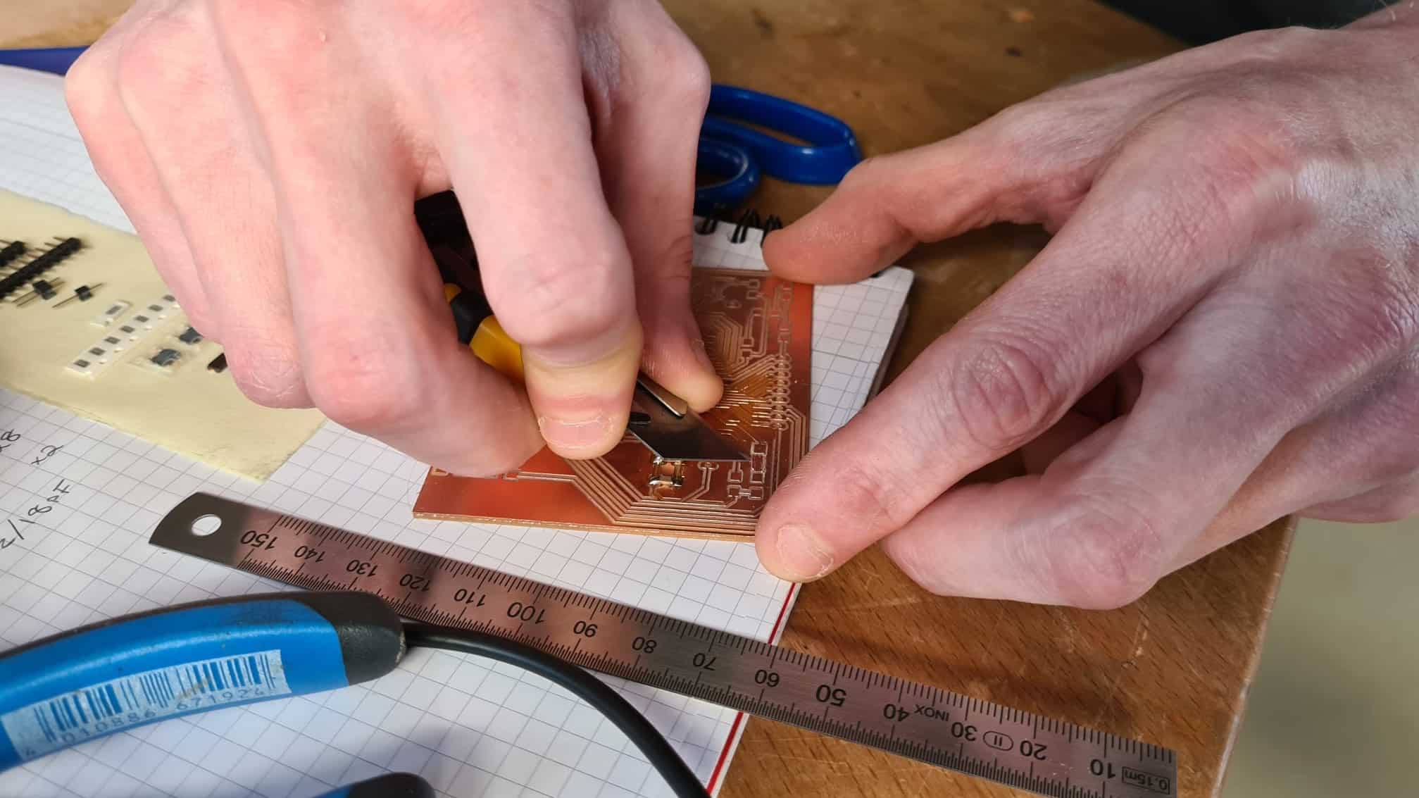
Soon after starting, the missing trace was FINALLY noticed and the haunting began. Thankfully I still had some material between the two pads that were meant to be connected, but unfortunately, the mill had already cut all the way around them both. The only option I could think of was to finish cutting the trace with a razor blade, and then to carefully bridge the gaps with solder.
Mistake No. 2
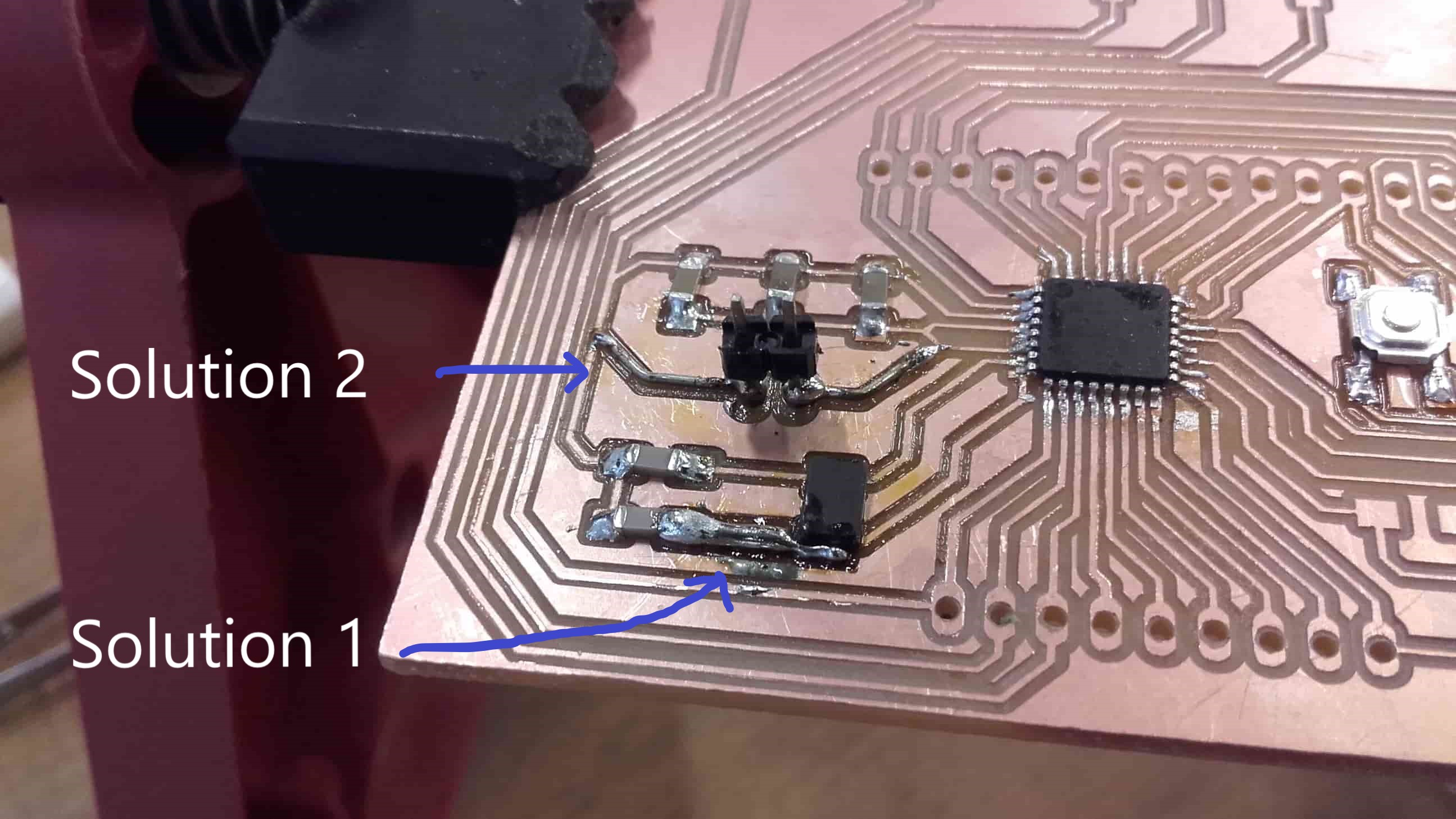
I also managed to completely mangle the installation of the 1x2 pinheader. I bumped it with the soldering iron and pulled up the very thin copper traces on both sides. I couldn't leave it that way, so I cut the traces where they were still connected to the board, and I used small jumper wires to bridge the long gaps. This was tedious, and I wished I had more hands throughout the whole process. These two solutions are pretty janky, but they worked in the end.
Checking and Double-checking
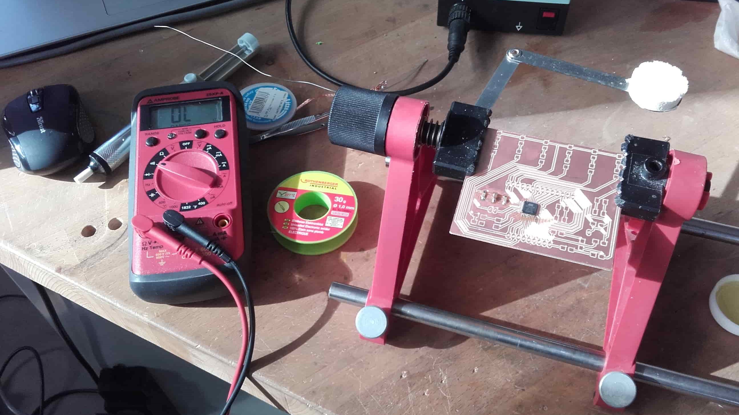
Problems aside, I carefully tested each connection for continuity where it should be, and a lack of it where it shouldn't be. The multimeter was also useful for orienting my diodes on the PCB.
Hero Shot
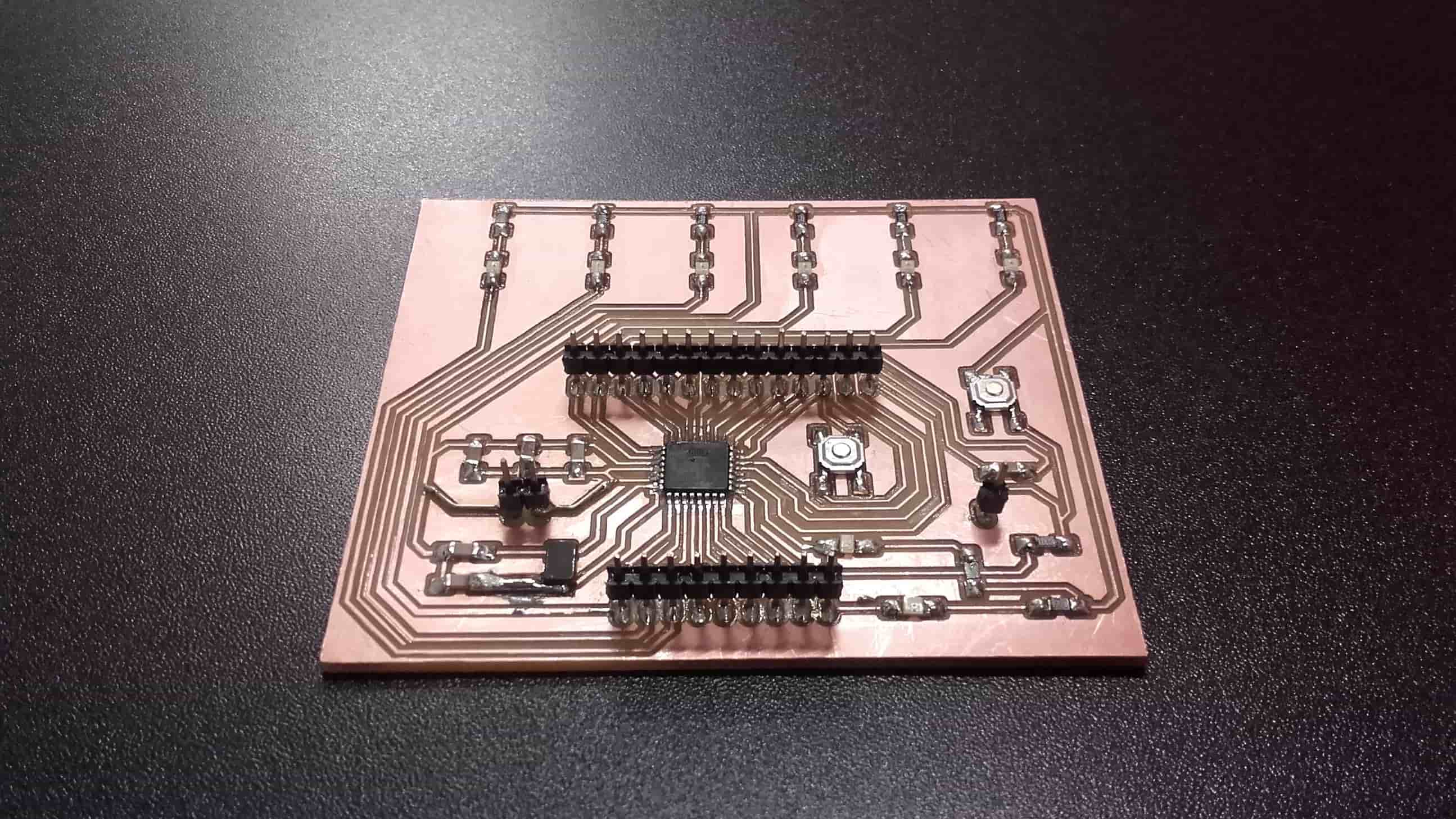
I am pretty happy with my work overall! This is a challenging board for somebody who has never made a PCB from scratch before...and the SMB components tested both my skill and my patience. I really hope it works! I am confident that the connections are good, but not noticing that missing trace really shook my confidence in the design itself. Fingers crossed!
Testing the Board
Hero Video 😀
To see me testing the board, check out the work I did for Embedded Programming week.
Hero Video No. 2
And also for Networking and Communications week.