5. Electronics production
This week Hero shot!

This week Checklist
- [✓] Linked to the group assignment page
- [✓] Documented how to made (mill, stuff, solder) the board
- [✓] Documented that my board is functional
- [✓] Explained and problems and how to fixed them
- [✓] Included hero shots of my board
Group assignment
This week, I work with my teammate Terry, Darren together to characterize the design rules for PCB production process: document feeds, speeds, plunge rate, depth of cut (traces and outline) and tooling. Please click here to see more details of our group assignment.
Individual assignments
This week I try to make an in-circuit programmer by mill, stuff and solder the PCB, then test it.
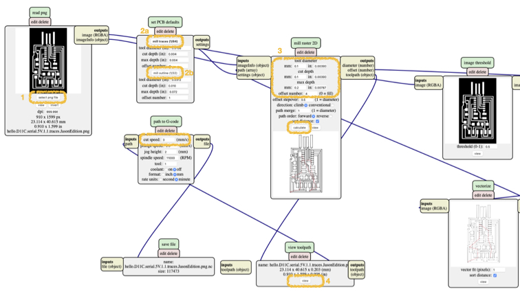
Convert traces and interior image for milling
Download the trace and outline image form Fab Academy first.
Then I will use Mods to generate .nc file form .png file.
▼ Go to Mods > Right click > programs > open server program > mill 2D PCB png.

▼ Many step and settings need pay attention.
- Select png file from computer
- Choose the PCB defaults for mill traces or mill outline
- Input tool diameter, cut depth, max depth, offset number, and calculate button. After calculate .nc will start download to your computer (Optionally you can change the cutting speed)
- You can press view button if you want to check the cutting path
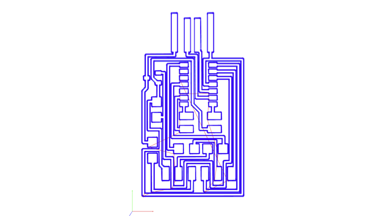
▼ This is the path of my .nc file.
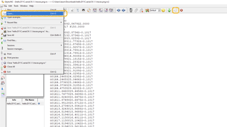
▼ After get .nc file, is time to connect milling machine! I used EdytorNC to do that. Please click Serial port configuration button on tool bar, then select Serial port, Baud rate, Data bit’s, Parity and Flow control for you machine.

▼ Then click Check serial port settings cutton on tool bar, and input some basic command to test the machine.
| Command | Fuction |
|---|---|
| % | Denote the beginning |
| m03 | Start the spindle turning clockwise |
| m05 | Stop the spindle |
| % | Denote the end |

▼ Now we can open .nc file, and press Send current file button on tool bar to send out the code, and waiting for the finished product!
For more information about operating milling machine, please click here to see more details of our group assignment.
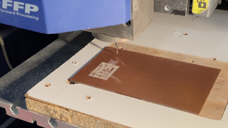
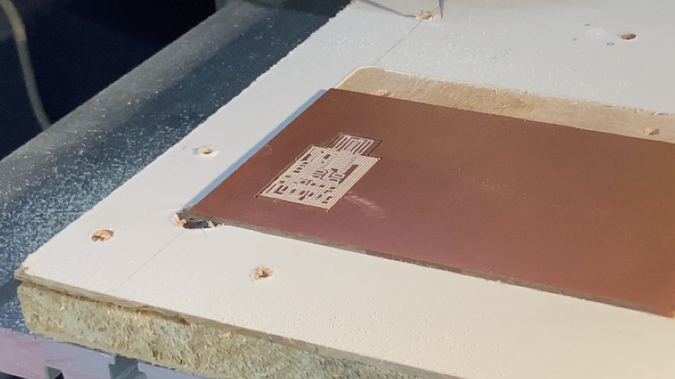
Milling PCB
▼ This is result of trace milling.
▼ This is result of outline milling.
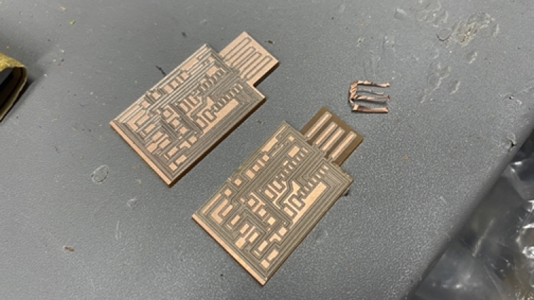
▼ Don’t forget use vacuum cleanner to clean after the milling.

▼ I use knife to remove extra copper. It decreases the situration short circuit when you stuffing the wrong components or wrong position.

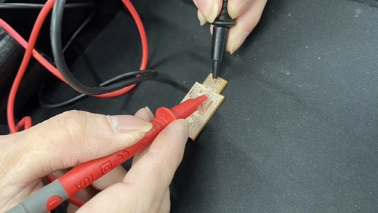
▼ I using multimeter to test the circuit and the component.
Stuff and Solder parts on PCB
▼ I using box to organize and place components.

▼ Let’s start stuff parts and solder!

▼ This is my first time use hot plate to solder.

▼ Yeah! I feels amazing to be able to solder such tiny components.
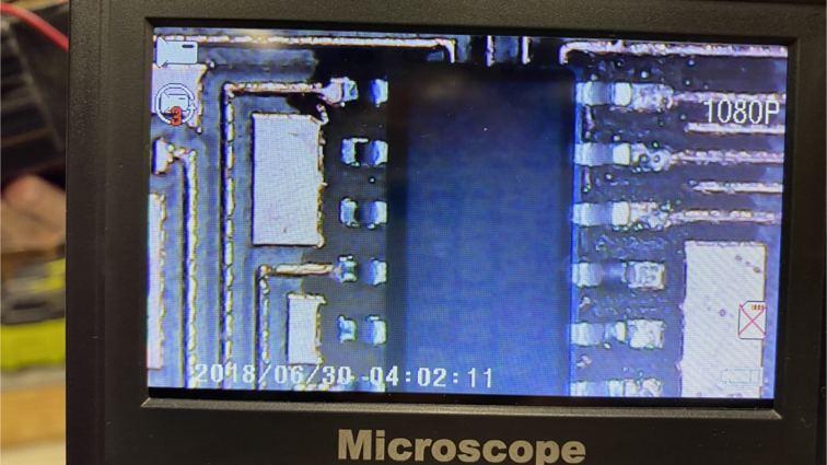
▼ I using multimeter to test. Also use microscope to check the outlook.
▼ Continue my work.

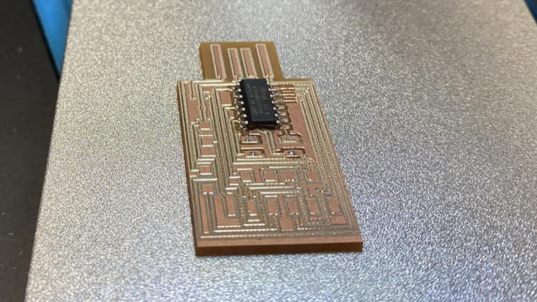
▼ Just Finish my first PCB.
▼ A small problem encountered in the production process is that the PCB board is too thin, resulting in poor contact when inserting to USB. The solution is to make it thicker.

Burn program to board
▼ Connect programmer to USB, and connect DIO, CLK, RST, GND between programmer and empty borad, also empty borad connect to USB port to get power (for safety, use USB hubs to connect empty board).

Download free_dap_d11c_mini.bin and edbg-windows-r29.exe first.
Open command prompt, go to path for you downloaded file, and enter command.
edbg-windows-r29.exe -ebpv -t samd11 -f free_dap_d11c_mini.bin
▼ This is a failed message.

▼ Yeah! download successful!

In command prompt enter command to check attached debugger.
edbg-windows-r29.exe -l
▼ There are 2 debuggers here! that mean my empty board have firmwire too.
- CMSIS-DAP is programmer provide by our FabLab
- Alex Taradov Generic CMSIS-DAP Adapter is my board

Useful link and downloads
Mods (Gen .nc file from image)
http://mods.cba.mit.edu
EdytorNC (Communicate with milling machine)
https://sourceforge.net/projects/edytornc
Burn program to board
free_dap_d11c_mini.bin
edbg-windows-r29.exe
Jason’s Edition PCB traces file
traces png file