6. Electronics design
This week I designed a simple I/O board that contains a button and an LED to demo input and output functions of the SAMD11C chip.
Chosen Software
Autodesk Fusion 360 The reason I choose Fusion 360 is because I was a EAGLE user. Fusion 360 acquires EAGLE to allow users design their PCB on it. I could design mechanical parts like enclosures of the PCB without switching between different softwares.
Preparation
- Download fab.dru and fab.lbr from this repo
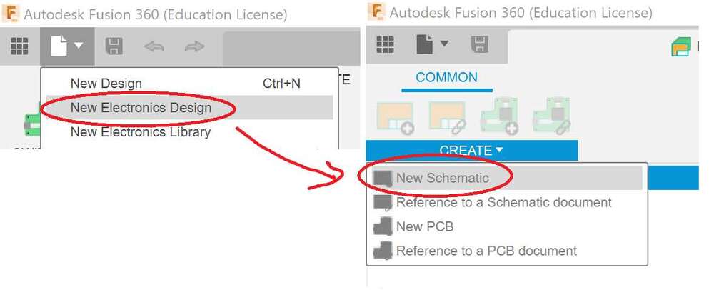
- Create a new Electronic Design from File menu, then create a New Schematic.
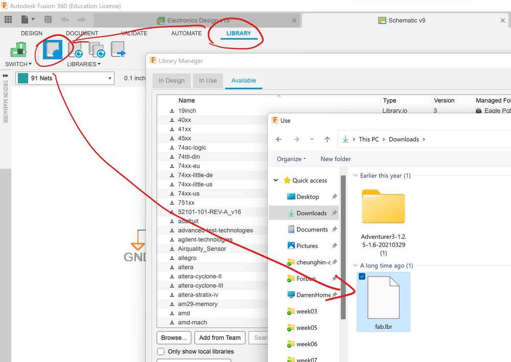
- Switch to LIBRARY tab, then open library manager by clicking the icon on the upper left. Then click the Browse button in the Available tab. Choose the fab.lbr file from step 1. This library contains the most components I need in Fab Academy.
Drawing The Schematic
-
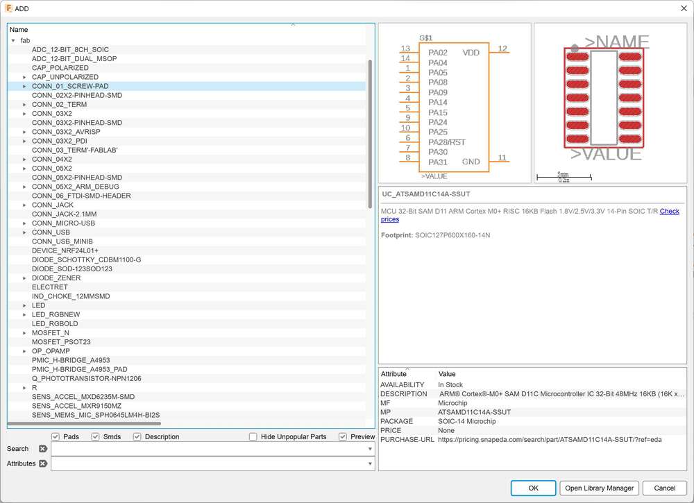
Add components from the library: Instead of choosing parts from fab library, I tried to select components from other managed libraries. The reason is they have 3D models of the components. I could render a more realistic model in Fusion 360.
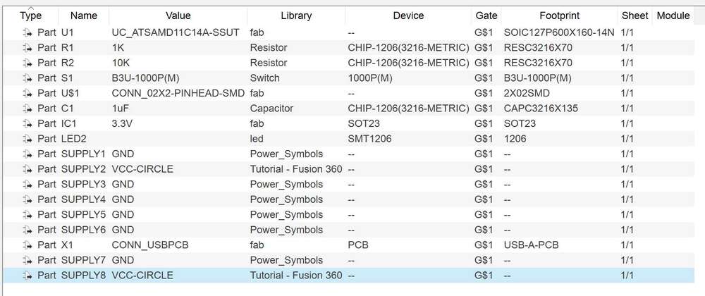
 A list of components I used in the IO board:
-
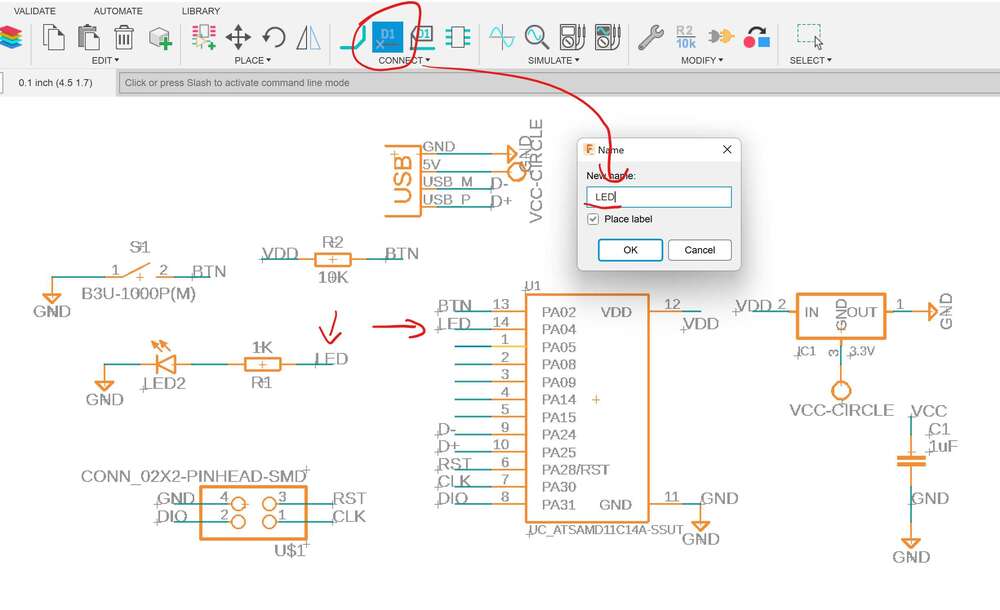
Connect signals: I first draw a short line from all pins of the components. Then change their signal name. By changing two or more signals to the same name, they will connect even there are no wire drawn between them. The LED was connected to PA04. The Button was connected to PA02, the other side of it was connected to GND. A 10k resistor was connected to PA02 to provide HIGH signal while the button was not being pressed.
Drawing The PCB
-
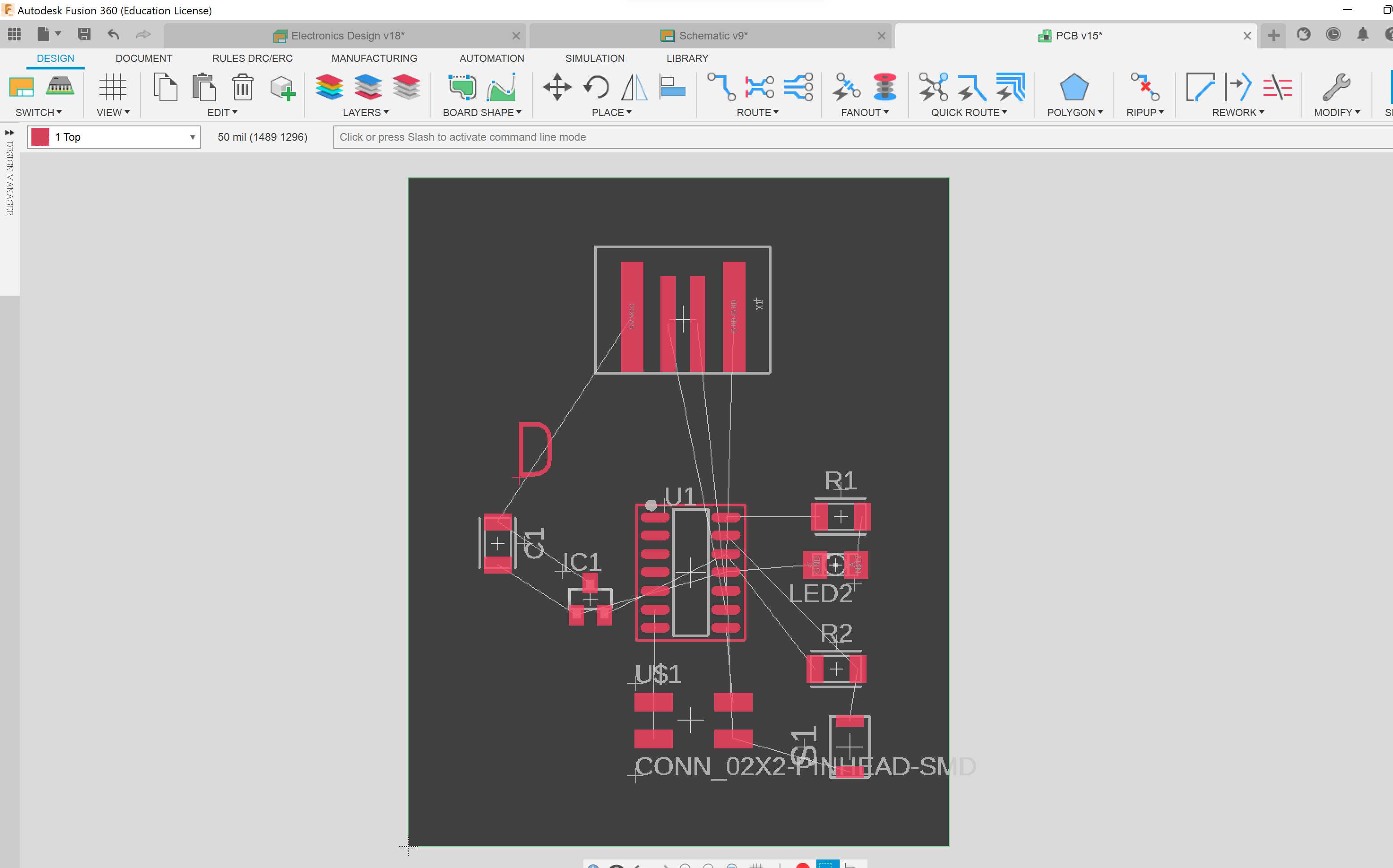
I pressed the Switch to PCB Document button on the top left corner. The software will create a PCB Document that will automatically sync with the schematic if there is not. Because I did not draw traces between components. There are air wires(white lines) indicating their relationship. I first move the components to the appropriate place. Because the SAMD11C chip is where all the signals will connected to, I place it at the center. Resistors, LED and the capacitor are placed around it. The USB connector was placed at the top and facing out.
-
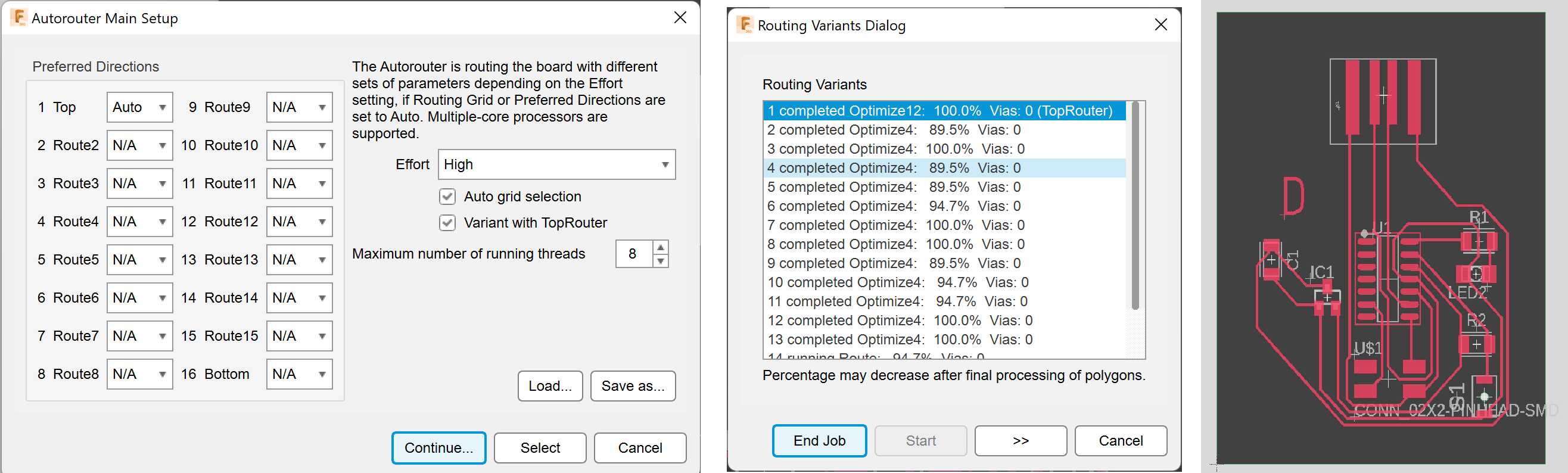
Route with Autorouter: I use Autorouter function to help me route the traces automatically, it finished the jobs in a few seconds. It provides different routing variants with different routing styles. The percentage shown means the completeness of the route. 100% means the variant finished all the signals needed to route. I choose a trace that looks good.
-
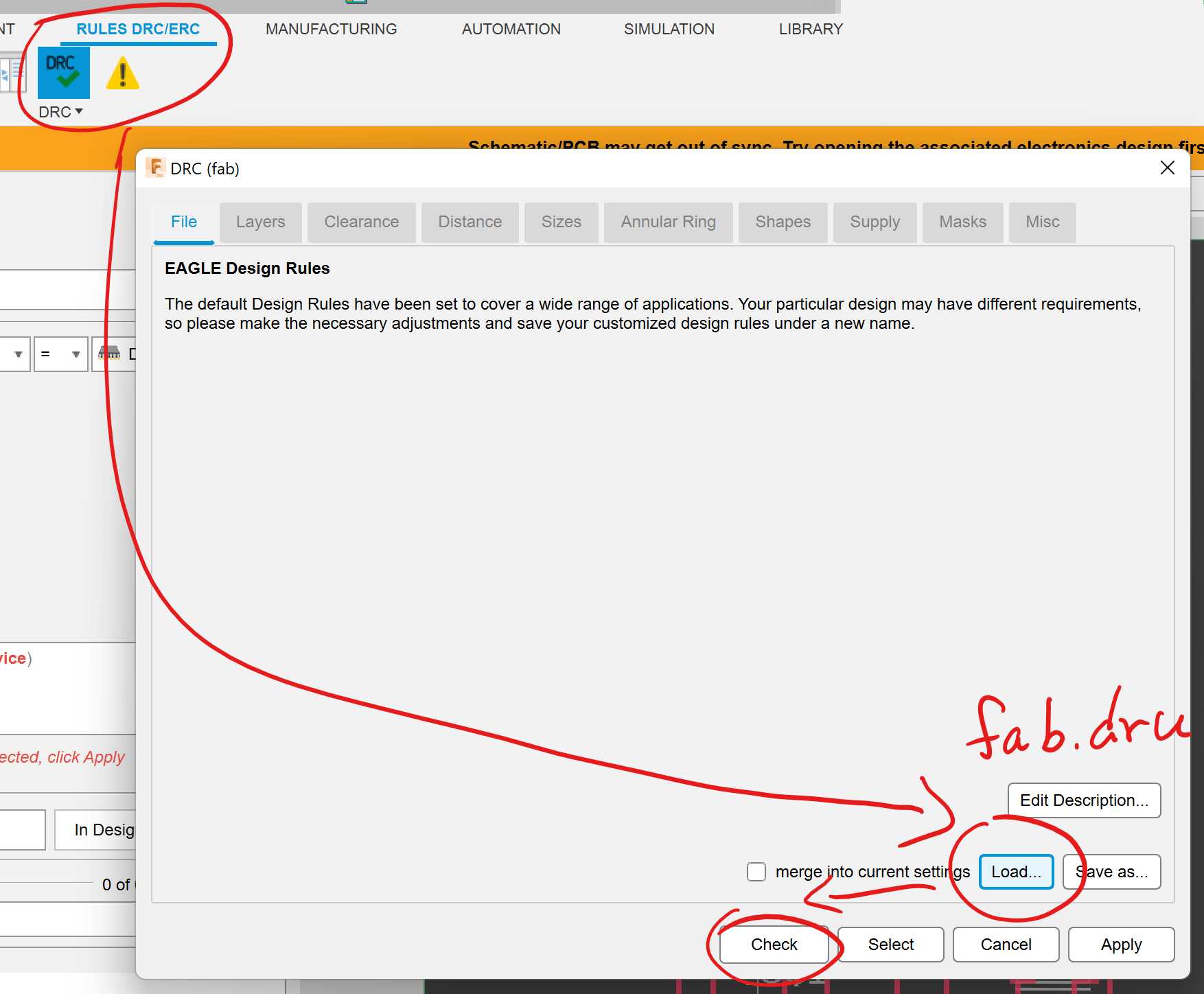
Run DRC Check: After routing the traces, I loaded fab.dru and run a DRC check to make sure the distances between traces are not too close.
-
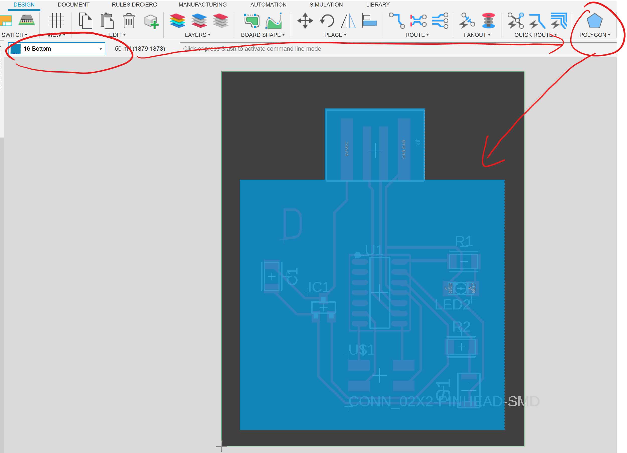
Drawing the PCB outline: I draw the PCB outline at Bottom layer, this is the only way I found to allows me export the image with a white outline projection on it. Please see the following image for details.
-
Export PNG files: Firstly hide all layers except the top layer. Then type export and hit Enter in the command line box. Choose Image to export the current displayed traces to image.
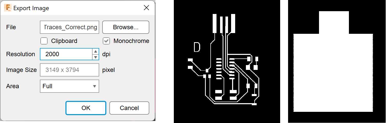
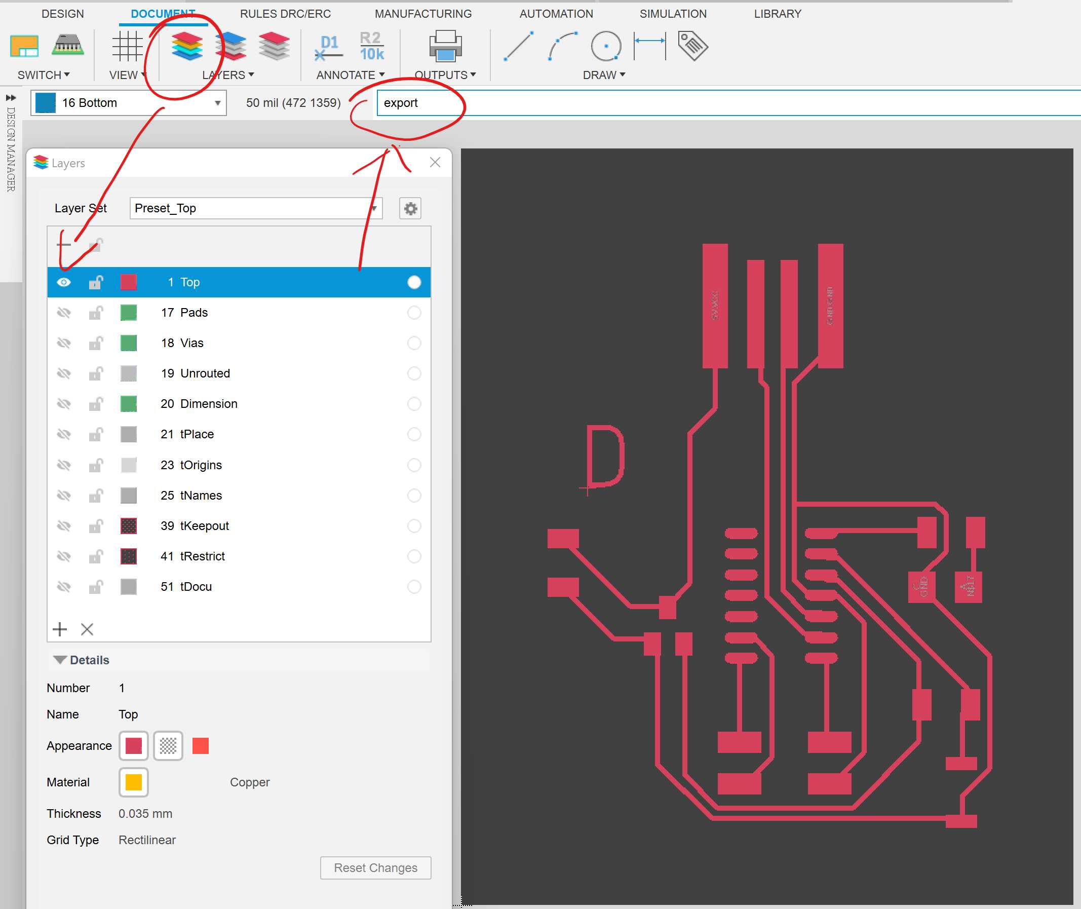 Select the filename, check the Monochrome option. Then set the resolution to 2000 dpi. Finally hit OK to export the trace image. Do the similar thing to the Bottom layer to export the outline image.
Milling and Soldering
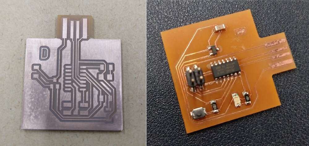
I converted the PNG trace and outline files to G-code on fab mods, then mill the pcb with a 0.1x10 degree bit. Then solder the components to the board with hot plate. You may refer to the Electronics production for detailed steps.
Programming
I firstly download the Arduino bootloader to the board using CMSIS-DAP Adapter I made in Electronics production. Then I wrote the program to test the LED and button on board.
void setup() {
  // set the pin modes
  pinMode(A4, OUTPUT);
  pinMode(A2, INPUT);
}

void loop() {
  // if button being pressed, blink the LED
  if (!digitalRead(A2))
  {
    analogWrite(A4, 256);
    delay(100);
    analogWrite(A4, 0);
    delay(100);
  }
  // if button not pressed, fade the LED
  else
  {
    for (int i = 0; i < 256; i++) {
      analogWrite(A4, i);
      delay(1);
    }
    for (int i = 256; i > 0; i--) {
      analogWrite(A4, i);
      delay(1);
    }
  }
}
The Results
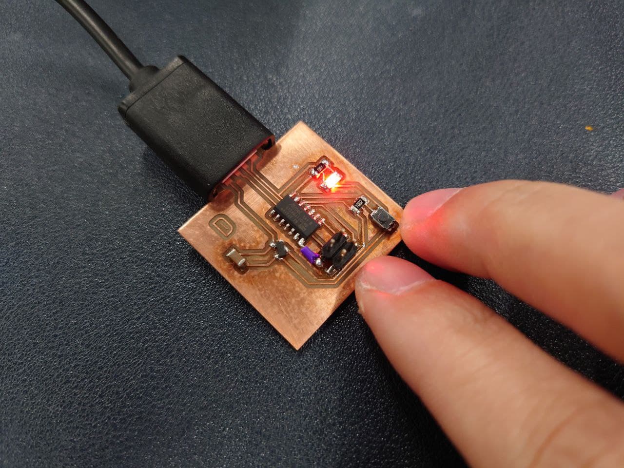
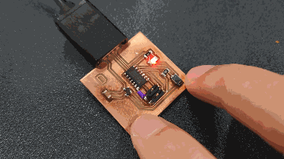
The LED fades between dark and light. While the button was being pressed, the LED will blink at 5Hz.
Problem Met
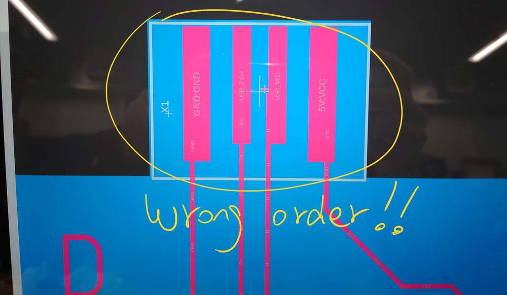
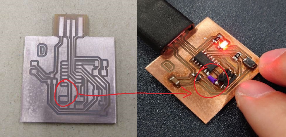
I used the USB-A-PCB foot print from the fab library. It allows me connecting the USB port without soldering a USB connector. But I placed the USB footprint upside down while routing the PCB. Because the USB pins on board are in reversed order, it will cause reversed polarty and failure in communitation when it is connect with the USB port. The worse thing is I realized the problem after milled and soldered the components on the board. Fortunately, I did not connect the wrong board to the computer before the problem was found. To fix the problem, I rotated the USB to correct order, re-route the traces and made a new PCB and transfer the components from the failed board.