6. Electronics design
Group Assignment Page
1 What is....?
As I don’t know anything about any thing. This will take a lot of time of research.
The websites where I took the information are linked in the tittle of every component:
1. VCC
Vcc of a bipolar junction transistor is the DC voltage that is supplied to the collector of the transistor. If VCC is too low, the transistor will not have enough power and the amplified AC signal will come out clipped. Vcc is a very important voltage when biasing the transistor because it determines how much the AC signal can be amplified to in the transistor…
2. GND
Ground, in the context of electronics, is the reference point for all signals or a common path in an electrical circuit where all of the voltages can be measured from. This is also called the common drain since the voltage measurement along it is zero.
4. Capacitor
A Capacitor is a passive component that has the ability to store the energy in the form of potential difference between its plates. It resists a sudden change in voltage. The charge is stored in the form of potential difference between two plates, which form to be positive and negative depending upon the direction of charge storage.
5. ATTINY45
The ATTINY45 is a low-power CMOS 8-bit microcontroller based on the AVR enhanced RISC architecture.
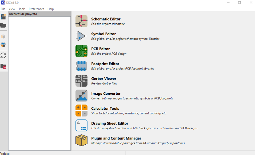
2 KiCad
I don’t have any knowledge about this, so what I’m starting to do is downloading KiCad.
KiCad is an open source software suite for Electronic Design Automation (EDA). The programs handle Schematic Capture, and PCB Layout with Gerber output. The suite runs on Windows, Linux and macOS and is licensed under GNU GPL v3.
3 Downloading KiCad
As this is a new software for me, and because of the many libraries that it has I decieded to documentate this, for the purpose of my learning
I deceided to download the CERN version as I know it for the name of the European Organization for Nuclear Research.

- This is options are only for 64-bit, if you have a computer with 32-bit you need to do other steps.
I thought that I must pay something for the software, but it was just a donation. Although the waiting was long (around 45 minutes), I downloaded succesfully.


6.1.2 Installing KiCad
As I already had FreeCAD in my laptop it wasn’t necessary to download it again. It was more simple than I think.
I opened it and I just launched it with the recommended settings.
6.1.3 Learning about Kicad
| The first thing that I noticed is the variaty of tools that it has. |
|---|
 |
And honestly I didn’t understand anything of it, so I started to study from the old and trustfull Youtube.
Most of my documentation is going to be terminology that I’ve never heard before, and that is going to be taken from the video above:
-
PCB: It’s an acronym that stands for “printed circuit board”. It is a board or card that electrically connects and mechanically supports electrical components.
These connections are made with a series of conductive tracks or traces, usually copper. And this copper is laminated onto or in between sheets of non-conductive material, like fibreglass. -
SMT: It’s an acronym that stands for “Surface Mount Technology”. Is when the electronic components do not have leads that extend through the board. Instead, the components are placed and soldered on just one layer. It’s good when you’re producing hundreds of thousands of boards, but it can be a pain to solder by hand.
(Source: Youtube.com)
-
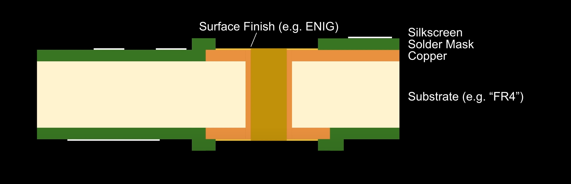
Substrate: is the rigid or semi-rigid material that holds everything together. (E.g. “FR4” The epoxy likely meets the flame retardant grade four standard).
-
Solder Mask Copper: Lacquer-like polymer that is only put on surfaces where we don’t want to solder components to.
-
Solder Mask Keepout: Coloured areas on a layer around things like pins and pads, places where we want exposed copper.
-
Surface Finish: This gives any exposed traces or pads a gold colour, makes soldering easier and helps protect the copper undernearth.
-
Silkscreen layer: It’s normally white, it helps to differenciate the components easier.
(Source: YOUTUBE.COM)
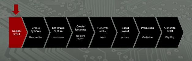
1) Design your circuit:
- Based on something you found online.
- Created in a simulator.
- Constructed on a bread board.
2) Create custom schematic symbols:
- If we can’t find some in the KiCad or DigiKey libraries
3) Draw the circuit in the software schematic capture program:
- It is known as eeschema in KiCad
- We can know reasearch the exact parts we need on DigiKey’s website.
From there we can look at each part’s datasheet to determine what the footprint should be.
4) Footprints:
- If we can’t find the footprints for our parts in the libraries, we’ll need to create our own using the KiCad footprint editor.
5) Generate netlist:
- We use cvpcb to associate schematic symbols with footprints
Still in eeschema, we generate a net list which is just a text document that tells which pins are electrically connected to other pins in the circuit.
6) Open up our board layout program a.k.a pcbnew
- Set up our design rules as specified by the PCB manufacturer, which we can usually find on their website.
- We then import our net list, which places our parts in the program. We move the parts around as we see fit and draw copper connections, known as traces between the necessary pins.
7) Production
- After that, we generate a set of files, known as gerbers, thar represent the various layers of the board we wish to make.
- We can use the “gerbview” program in KiCad to examine these files before we send them to the manufacturer.
8) Create a Bill of Materials, or BOM
- Order the electronic components from DigiKey.
-
Once all the parts arrive, we can solder them to the board to build the badge.
-
Check Chris Gammell’s tutorials on KiCad (Getting to Blinky 5.0)
- Go to forum.kicad.info to search for answers and ask the community if you get stuck.
6.1.4 Create a Schematic Symbol
I’m going to try to redraw the echo.hello.world board with an LED and a push button, but I’m going to remove the ISP ftdi component because I’m going to program it with a clip.

(Source: academy.cba.mit.edu)
Kicad New Project + Paths
| First, click on new project or press the shortcut |
|---|
ctrl+n |
 |
| After this we need to choose a folder that we want to save our KiCad projects together. |
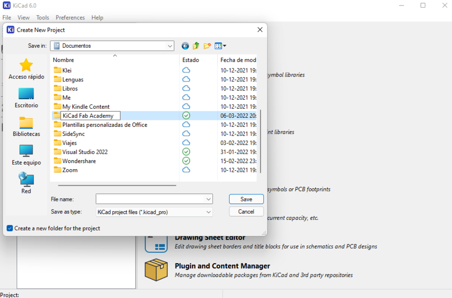 |
| Inside of this folder I’m going to create another folder called |
|---|
| “My first project”. |
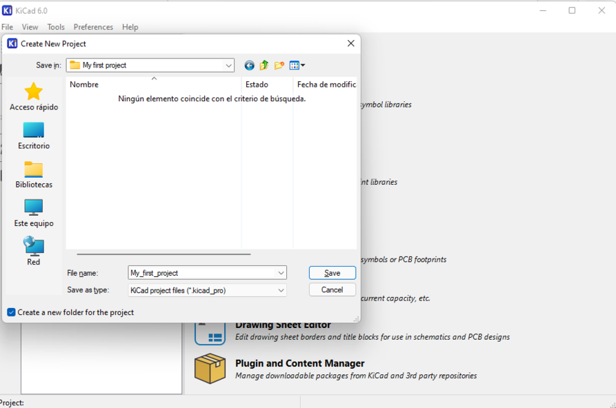 |
| After this the files of my project appeared on the left. |
|---|
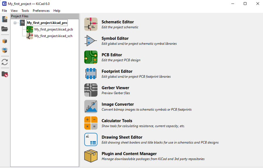 |
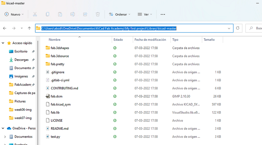
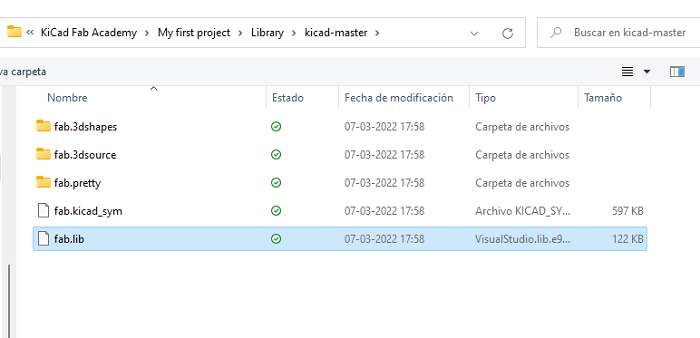
| I downloaded the files from gitlab.fabcloud and saved it in the directory of “KiCad Fab Academy” and inside of that one I put the files: |
|---|
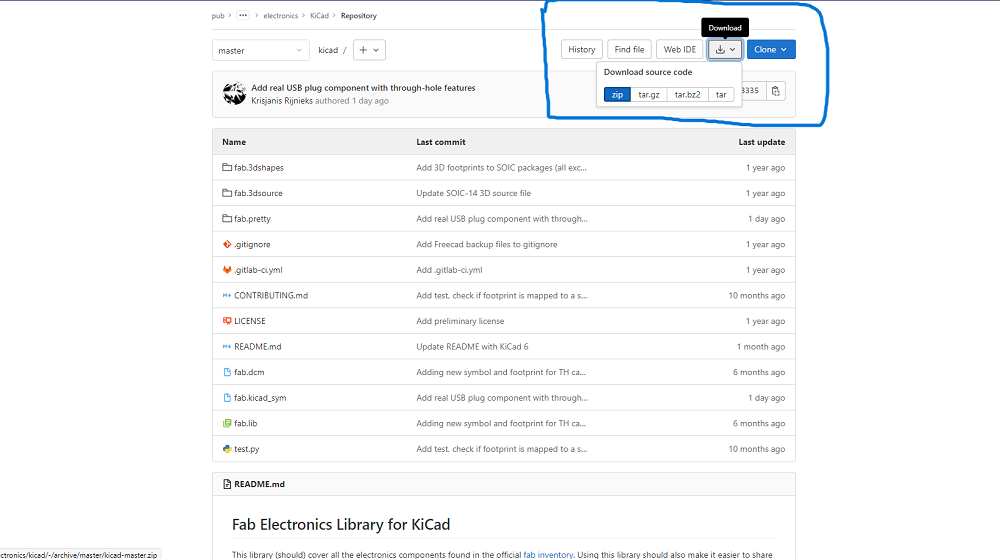 |
 |
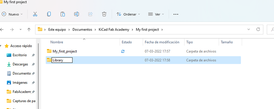
| I’m going to put every project in the folder of “KiCad Fab Academy“ |
|---|
 |
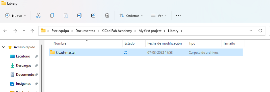
| Here I’m creating my new directories |
|---|
| KiCad Fab Academy>>My first project>>Librarykicad-master |
 |
 |
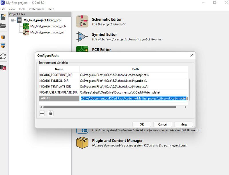
| After creating the directory, I’m going to copy the path of my folder so I can work with it. |
|---|
 |
| So we need to go to: |
|---|
| Preferences>>Configure Paths… |
|
| And then we put a name to it and paste the route |
|---|
 |
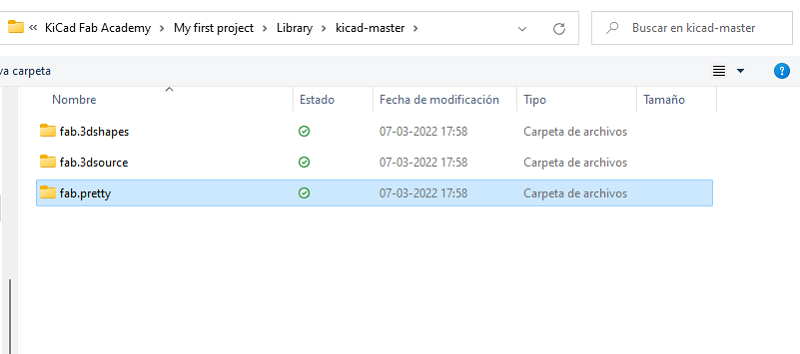
How to add new footprints?
Install the Fab Lab related libraries.
This is in the case you can to use Fab Libraries, but in my case, that library didn’t have the correct size of the footprint for the ATtiny45 that I wanted to use
The video will help you a lot to add the library of Fab Lab. I’ve found it very helpful and well-explained.
How to choose the right Resistor?
This was a nightmare for me, luckily I found a very good explanation about it in a website of Autodesk
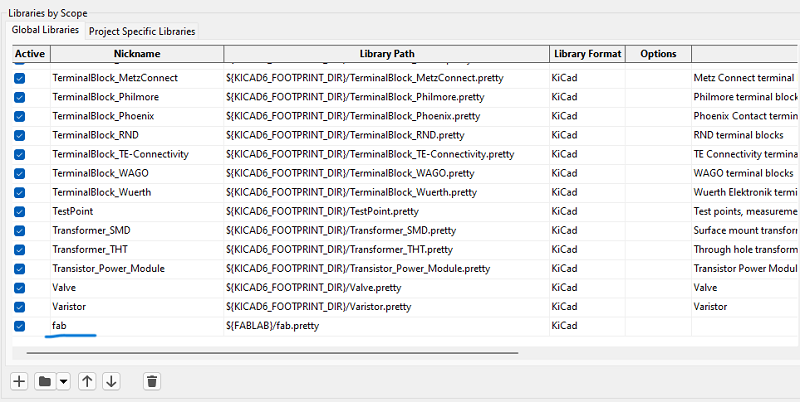
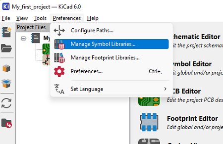
1. Manage footprint libraries
| Click here and another window will appear with the footprint libraries |
|---|
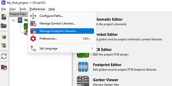 |
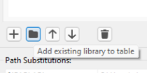
| We need to add the footprint of Fab Academy that we previously added to our folder. |
|---|
| We are looking for this: |
“fab.pretty“ |
| For this click on the icon of the folder that says |
“Add existing library to table“ |
 |
 |
| Once we get it we click |
|---|
OK |
 |
2. Manage symbol libraries
| For this we need to do the same as before but now, we are looking for the symbol: |
|---|
fab.lib |
 |
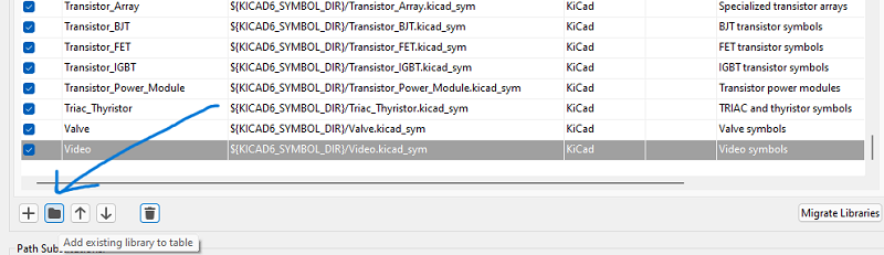 |
 |
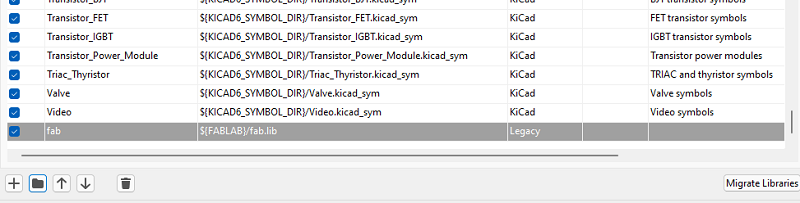 |
Click OK and the windows will close.
Don’t worry if it freezes, it will take a bit.
6.1.5 Drawing the circuit schematic
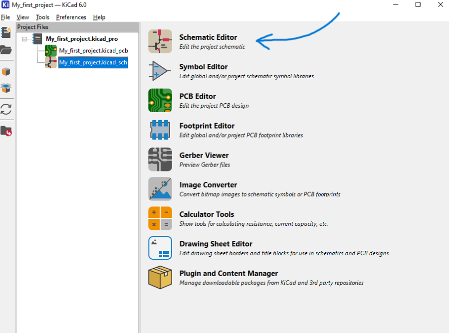
You will have two files, we are going to work with the one that ends with .sch
Click on Schematic Editor, the one that looks like this:
ERROR 6.1.5.1 Horizontal Green Lines
| If by any reason, you open the editor and it looks like this: |
|---|
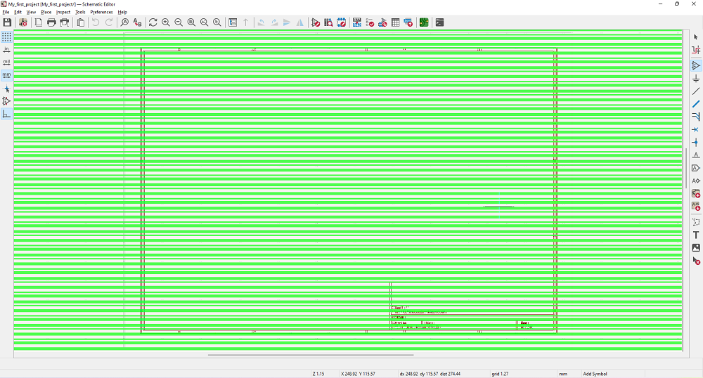 |
| It’s because you need to update your drivers of your graphic card |
| SOLUTION |
6.1.5 (Continuation)
| Now that the error is fixed we go to the following path: |
|---|
Place>>Add Symbol (A) |
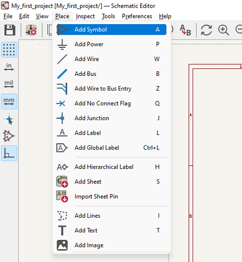 |
Once another window is opened, we need to put our components here, these are the components that we need to put in the editor. So I just type them into this box one by one.
In my case, fab libraries had a problem with the libraries, it didn’t show the correct library for my microcomponent. So I had to use the footprints that come by default on KiCAD.
Now that you found the one that you want, just drag it wherever you want and left-click to put it.
Important note
KiCad is only a designing program and it doesn’t matter what values or “names” you put for the symbols.
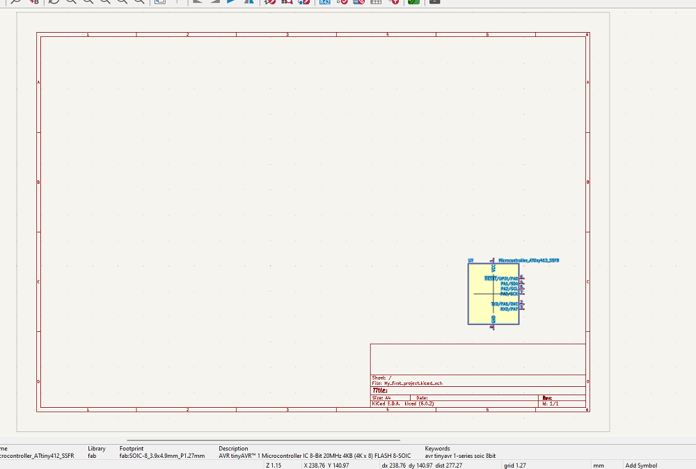
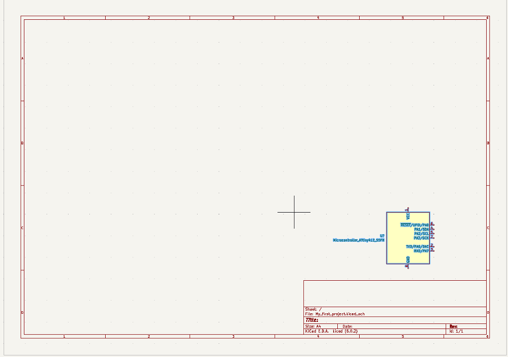
Once we have every symbol or component it should look like this.
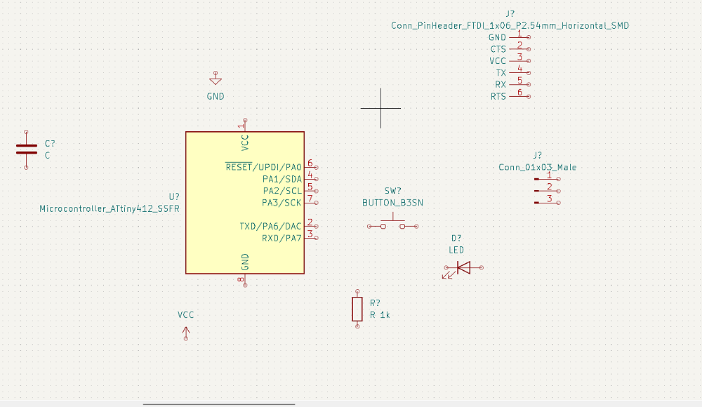
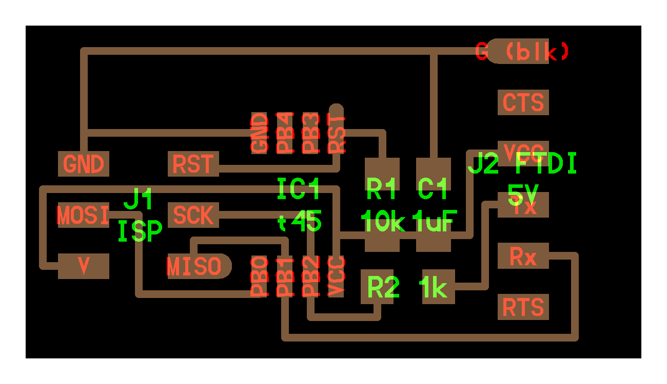
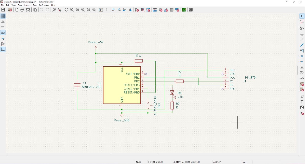
For have an idea of how to connect the components, I followed Neil’s board:
I had some minor mistakes in the schematic, like for exampling putting an ATtiny412 instead of and ATtiny45.
I even changed the name of my project to pepper
So after some minor changes I had something like this that I’m going to explain how I did it:
To connect the components I used this tool that says “Add a wire”:
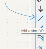
For adding the different symbols, click on “Add Symbol”, or just press the key-letter “A”:
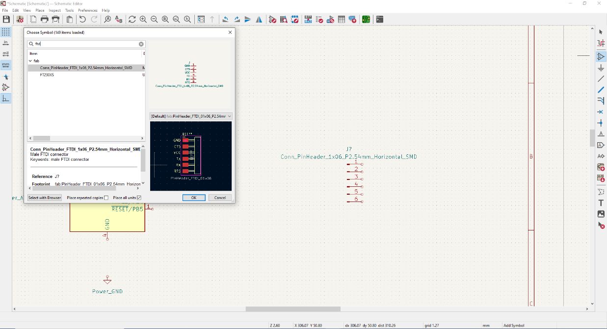
| For changing the name or the “value” and other things, you can select the name of the symbol that you want, and do the following: |
|---|
Right-click >> Edit Value (V) |
| There you can change the name. |
 |
| Once you have everything set up, you need to annotate the schematics. For this go to: |
|---|
Tools >> Annotate schematics |
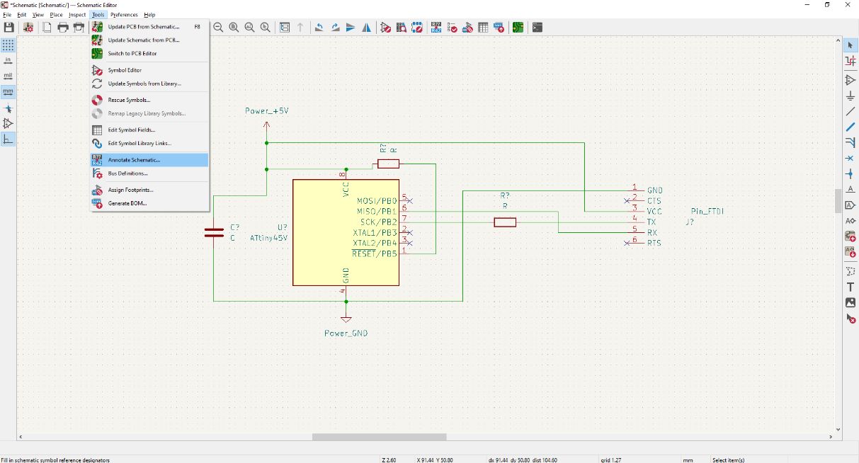 |
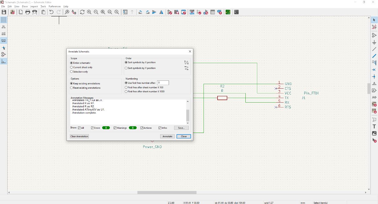 |
| This will make your symbols to have different values. For example if you have two resistors, one will be R1 and the other one R2. |
| Once everything is well made, I clicked on the green button on the top. Where it says “Open PCB in board editor” |
|---|
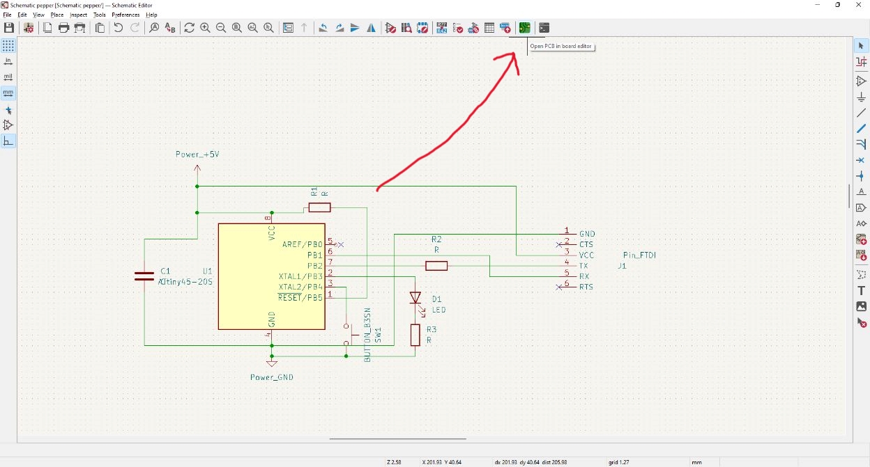 |
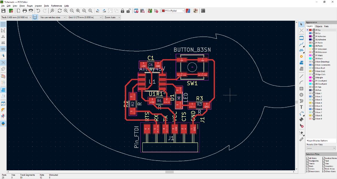
This part can be a bit confusing, but it is very simple. You have to attach every white (or yellow) line that the schematic shows with every component.
| Should look something like this: |
|---|
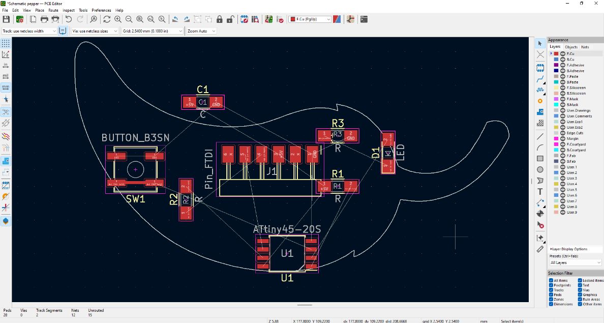 |
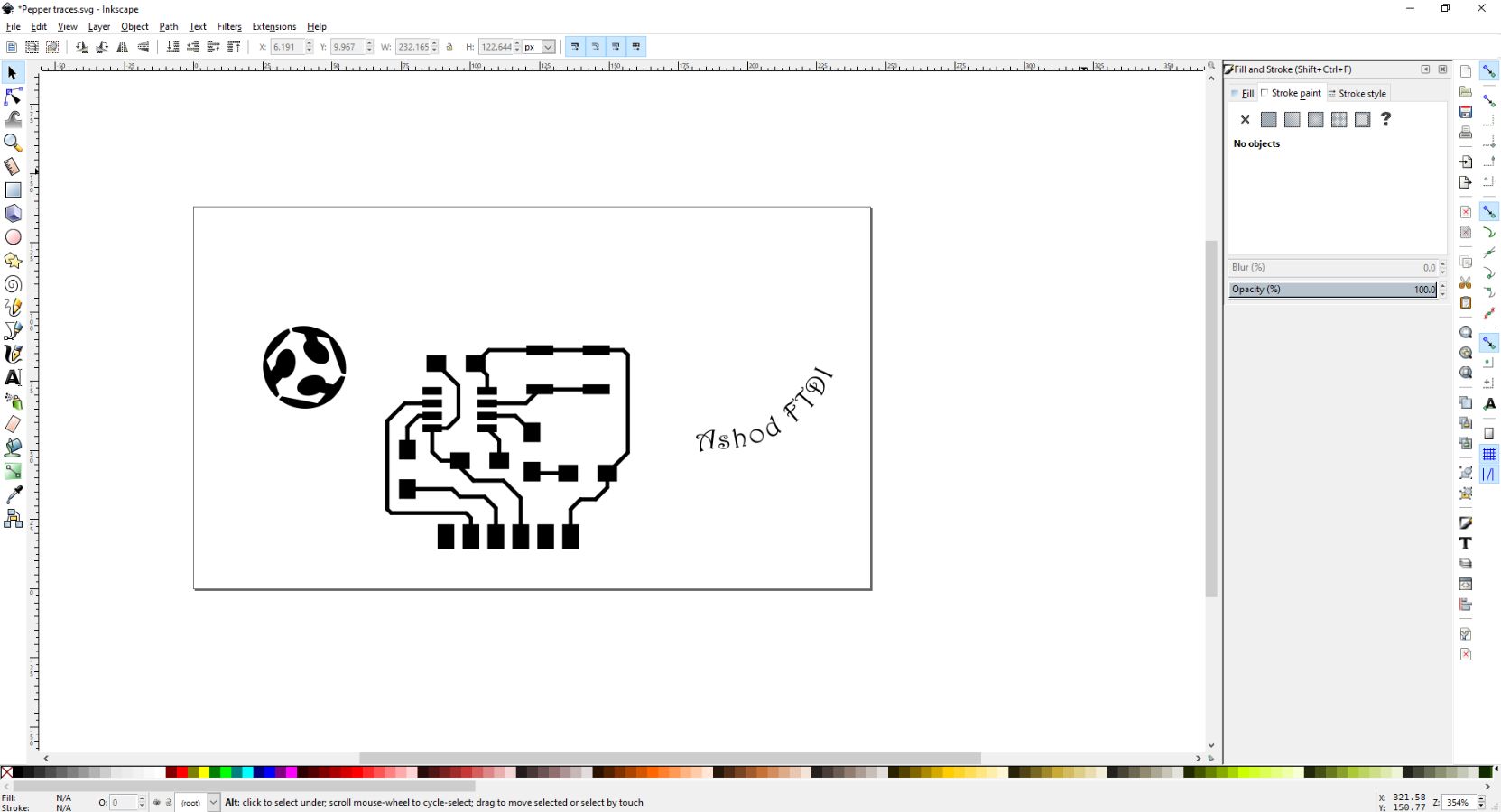
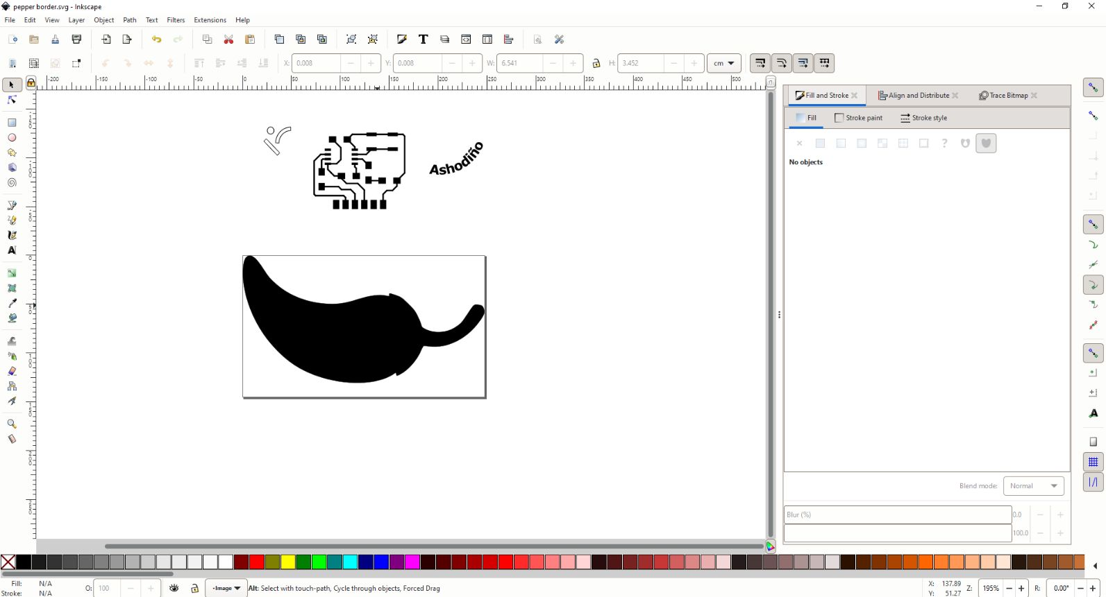
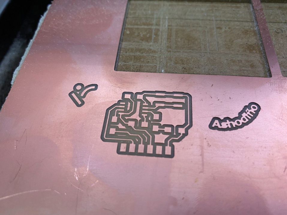
You can see that I have a “Chilli Pepper” in the background.
| For this I just search on google and I took this picture as reference. |
|---|
 |
| (Source: ClipartMax.com) |
Later I opened the image on Inkscape and I transformed into a vector image.
| And if you are asking how to add the vector image to KiCAD simply follow this tutorial. I used Inkscape for this method. |
|---|
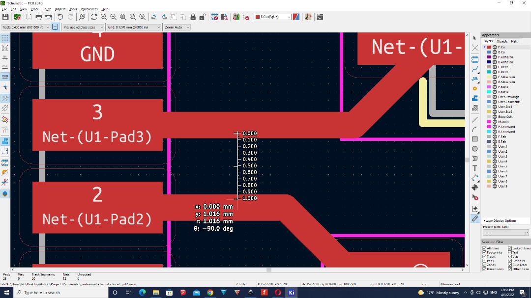
Once I finished to tidy every component, I added the wires to connect the different components.
| For adding the wires you need to press (x) or click on this logo: |
|---|
 |
| This is the final result |
|---|
 |
Important note
And as well, I had to be careful with the wires. Because the distance between the wires must NOT go below 0.4mm because of the measures of the printing rules that we did for the group assignment for the Electronic Production week.
 |
|---|
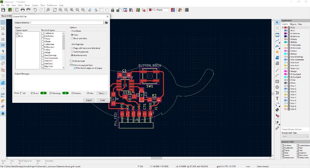
Once everything was good I exported it as .svg file and imported it on Inkscape for adding more designs and later to have the traces and the interiors of the PCB. |
|---|
 |
6.2 Editing in Inkscape
After exporting it as .svg, I opened the file on Inkscape, here I modified it. For example I added the logo of Fab Lab and I added my name on it.
Before doing this I had to watch a couple of videos:
Watch this video to know how to vectorize a PNG Logo with Inkscape:
And watch this video to know how to make curved text in Inkscape:
Then I started doing my editions:
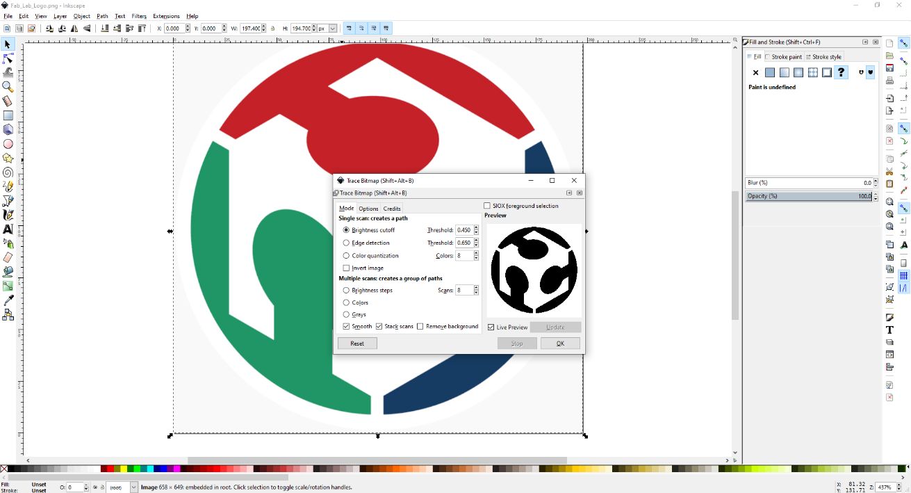
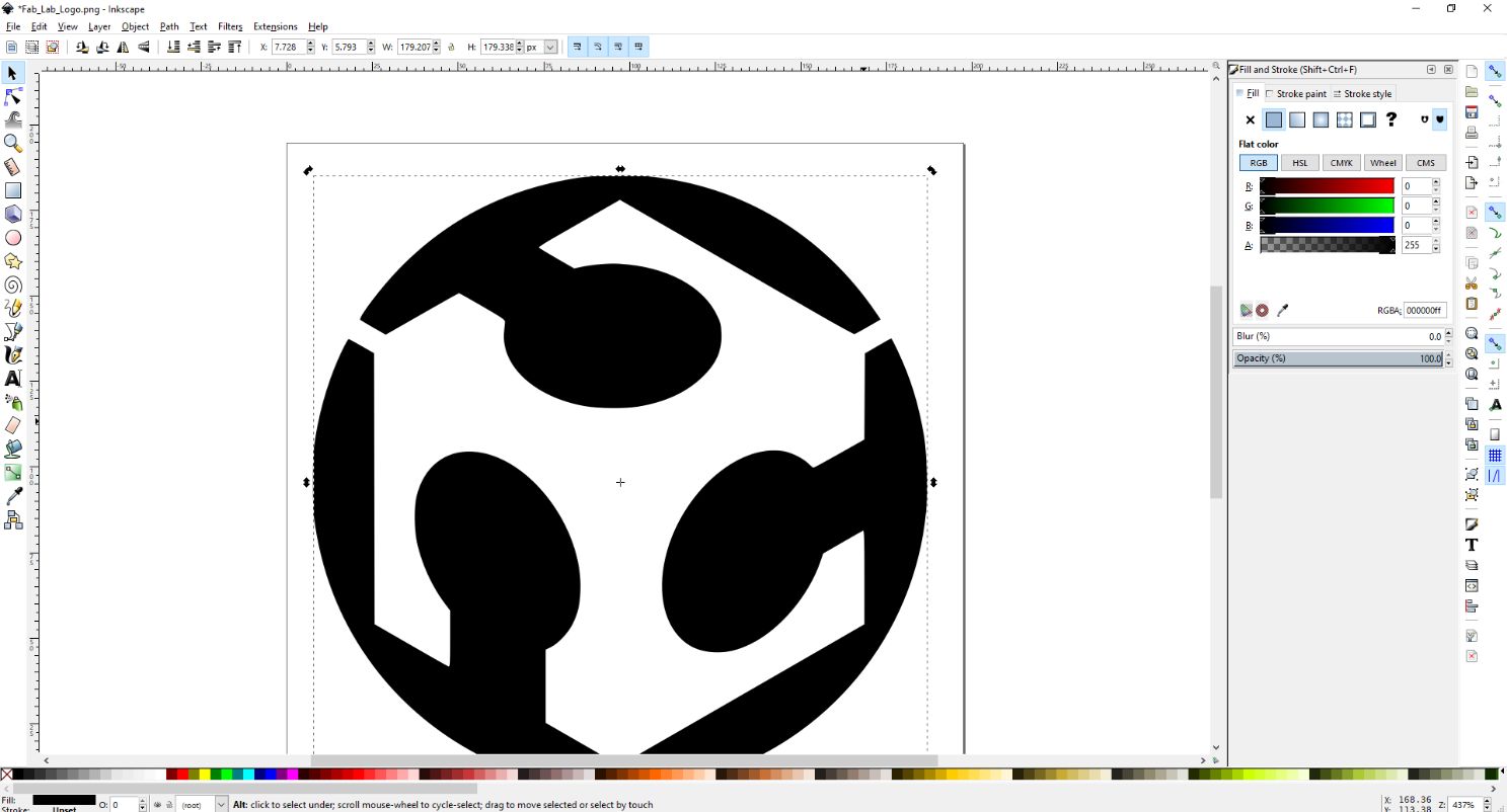
| First I import the Fab Lab logo from internet, and I converted it into “BitMap” |
|---|
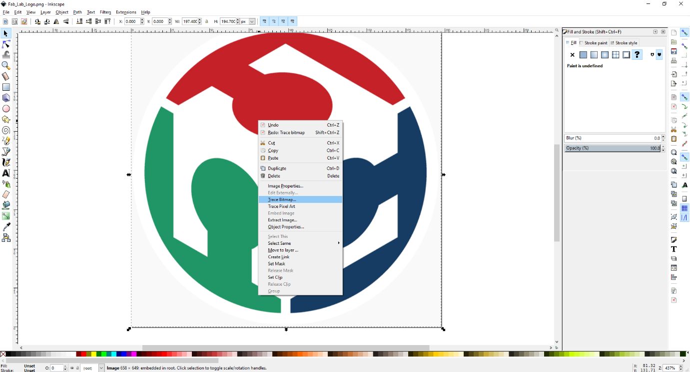 |
 |
 |
 |
After this I put it on the design and I started to work on the text.
For this I just followed the video that I mentioned before.
| After some editions I had this result: |
|---|
 |
 |
6.3 Using End-mill Machine
When everything was ready, I exported two files:
- One for the traces.
- One for the interior.
| So what I did on Inkscape was to separate into two designs. |
|---|
 |
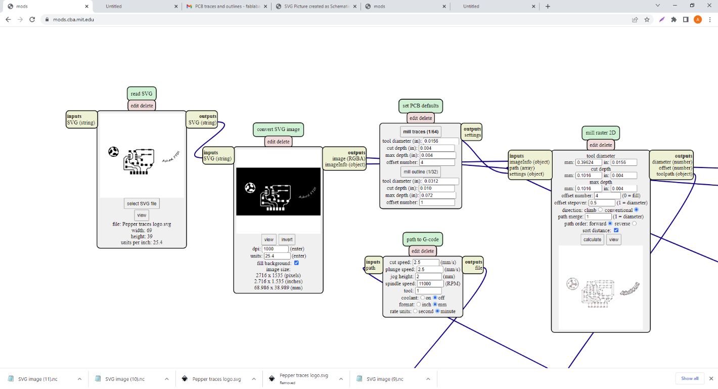
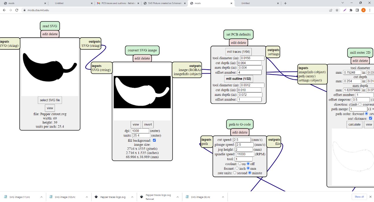
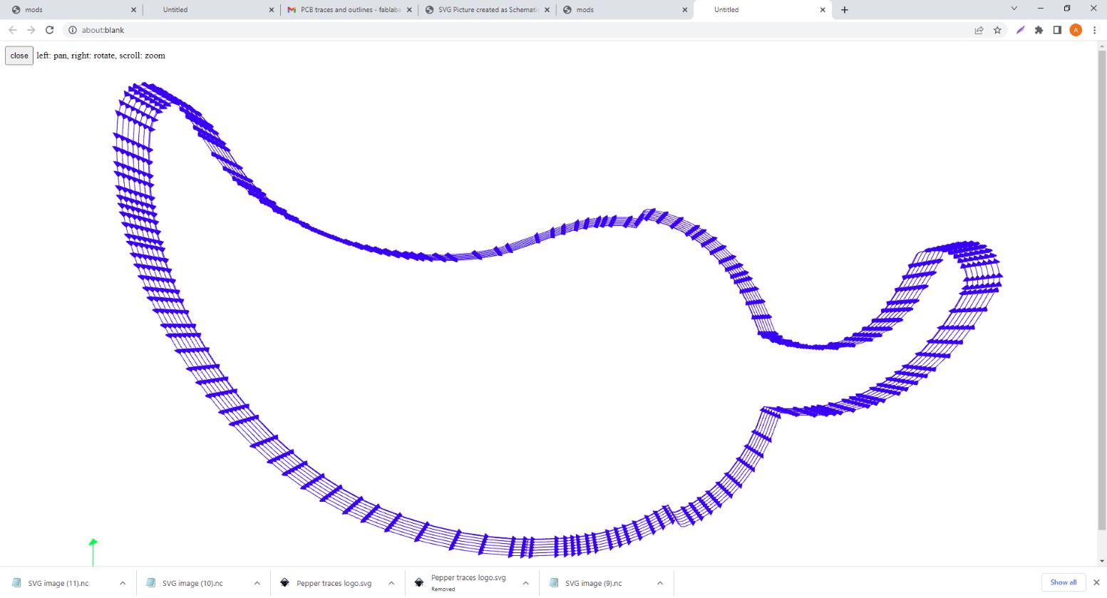
| And then I exported my both files .svg to FabMods |
|---|
| First, I opened the interior and selected the parameters for the 1/64 end mill. |
 |
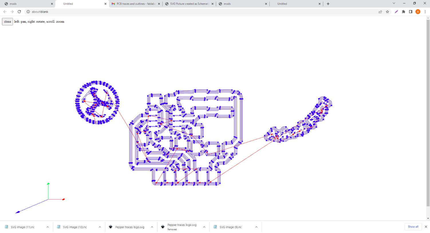
| And I had this result: |
 |
| -------------------------- |
| I did the same with the traces but changing the 1/64 for 1/32 |
| -------------------------- |
 |
 |
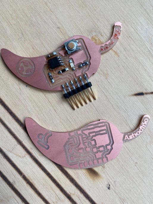
Then I soldered it and I tried to program it.
But unfortunatelly something happened....
6.3.1 Fixing the PCB
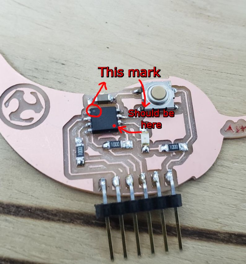
When I tried to program it, the place started to smell something was getting burnt, but I didn’t notice any smoke. As I was programming with a clip, this one jumped from the position of the microcomponent (ATtiny45), and because of the heat, the ATtiny45 got unsolder.
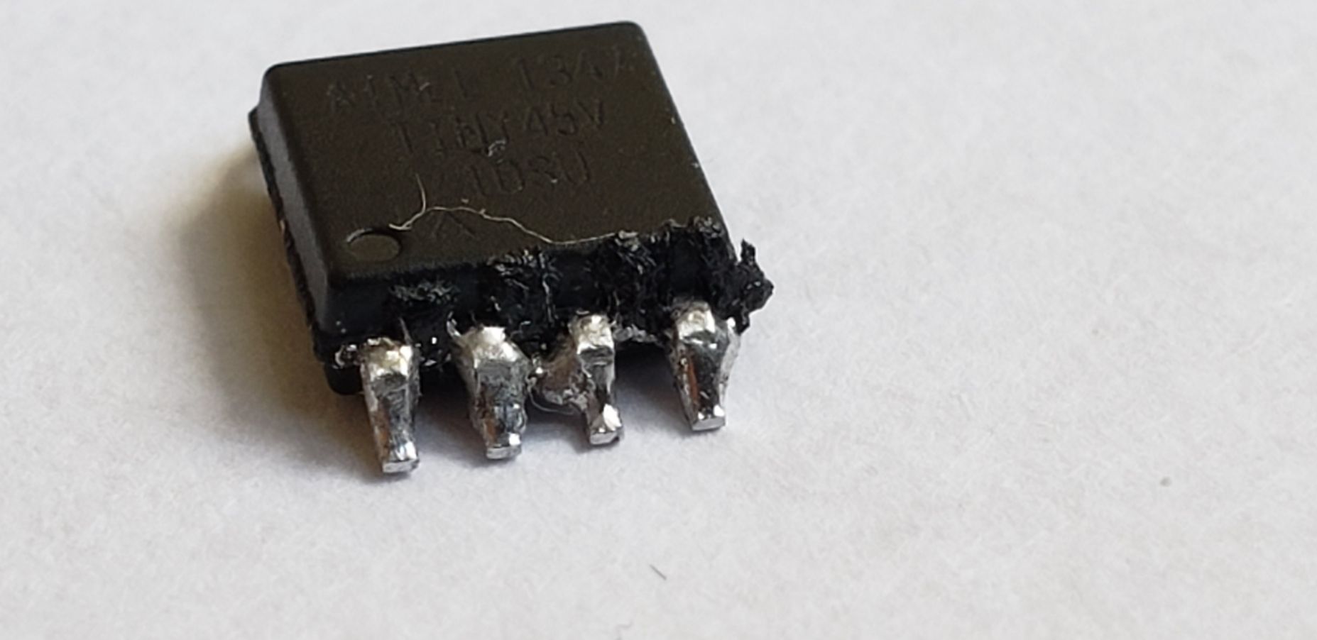
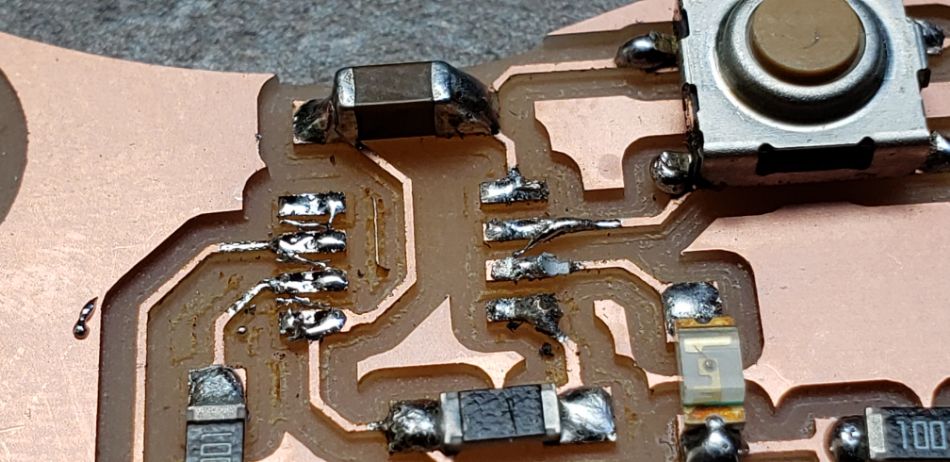
The problem was that the microchip was soldered upside down. Basically the RESET button must be connected to the 5V, but as it was soldered incorrectly, the RESET button was going nowhere.
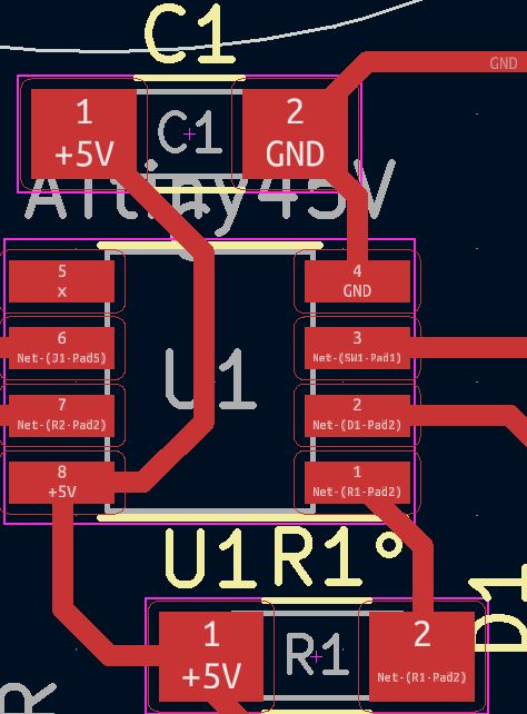
You can see in the schematic how it should go from the beginning:
And this is how I soldered it upside-down:
Fortunatelly, the programmer didn’t receive any damage:
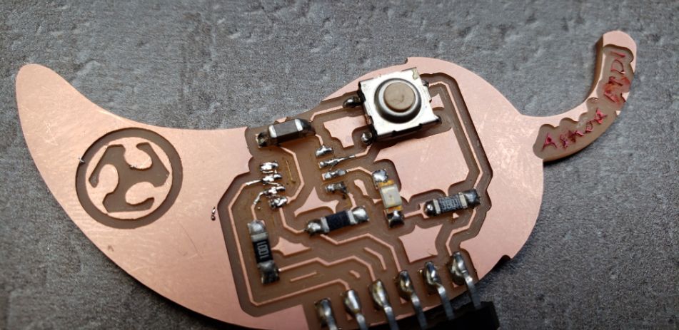
7. Building the right PCB
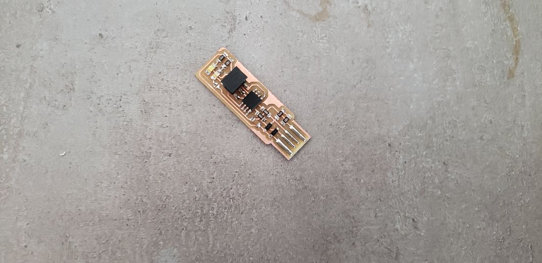
After the failure I tried to design it again because I took an Attiny45 footprint that was not the correct one (it had smaller legs).
I also changed the logo of Fab Academy to Fab Academy Dilijan.
 |
|---|
For the next steps I did the same for this PCB. This is:
| 1. FabMods (traces and interior) |
|---|
 |
| 2. Milling |
|---|
 |
| 3. Soldering (correctly this time) |
|---|
| I had to change the components from the old PCB to the new one |
 |
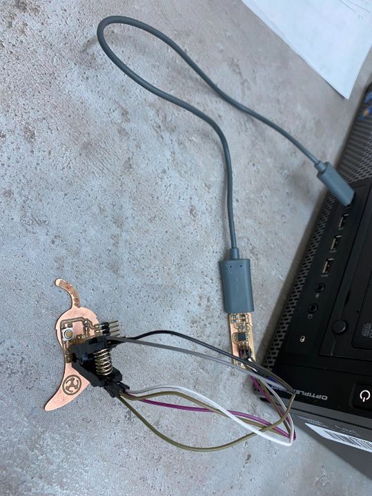
8. How did I program it?
Well this question is a very good one as I don’t have any ISP pin.
| What I wanted to do in the beginning was to use a programmer clip like this: |
|---|
 |
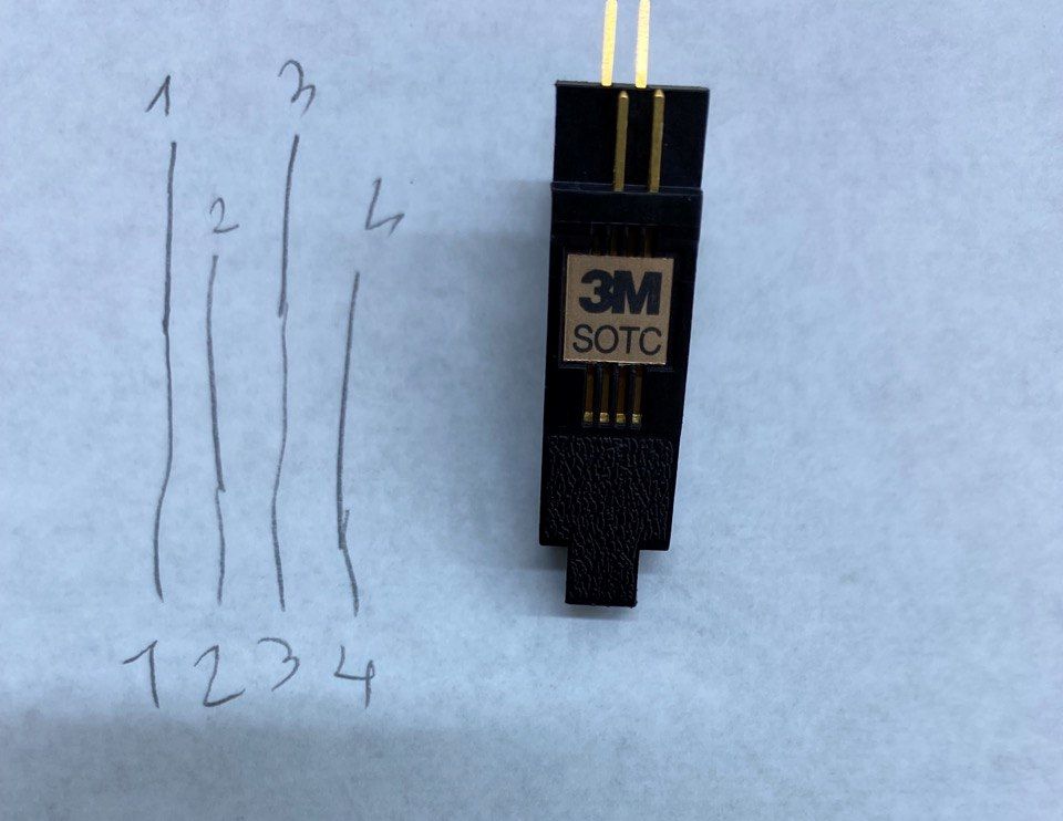
| So what I did was to look for the PINOUT of the Attiny45 and the ISP of the programmer |
|---|
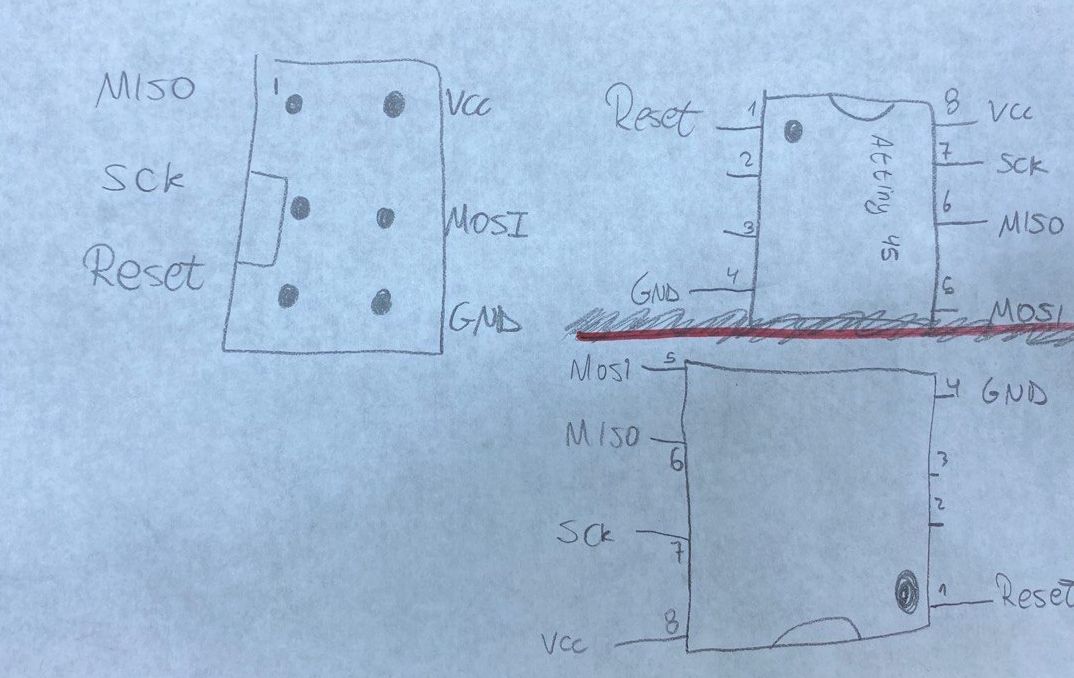 |
| And as well the position of the “teeth” of the clip |
|---|
 |
| Once everything was clear, I “clipped” it |
|---|
 |
 |
 |
 |
| Unfortunatelly, it seems that I put too much soldering material. So the clip teeth’s got wasted, as it didn’t grab it well. |
|---|
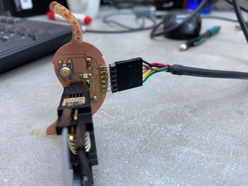
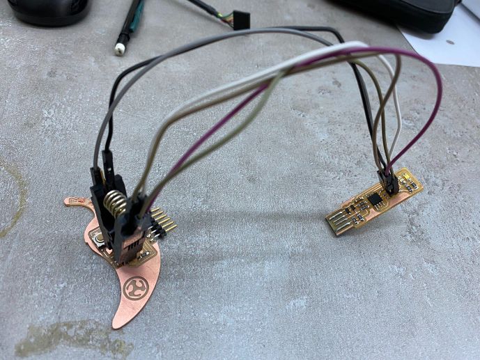
For this reason I had to go to another level and make a FRANKESTEIN.
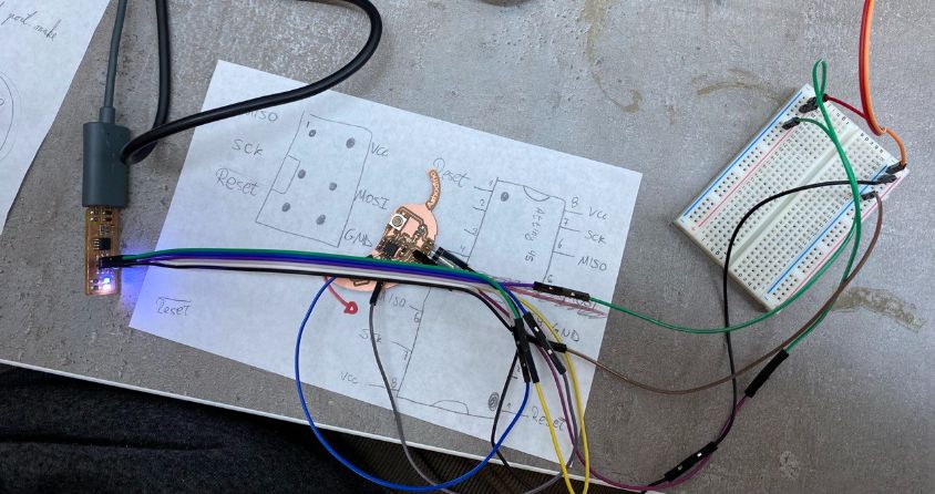 |
|---|
I did this with the help of my instructor.
Basically, instead of having the connections between the MCU and the clip, I had to connect directly the pins to the MCU legs to the programmer.
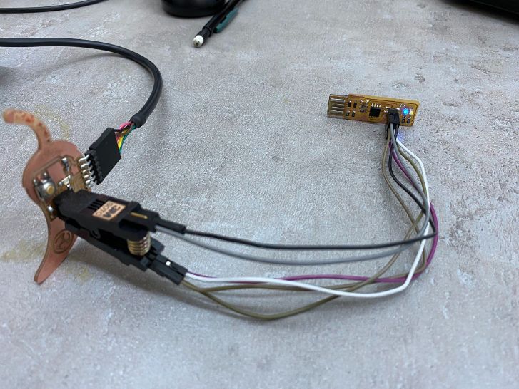
Once everything was correct, I could program without any problem, because the connections didn’t have any problem.
We tested the blink LED first:
8.1 Code
//
//
// dispenser.45.c
//
// simple software to turn a fogger on/off with delay
//
// Babken Chugaszyan
// 04/05/2020
//
// (c) Babken Chugaszyan 2020
// This work may be reproduced, modified, distributed,
// performed, and displayed for any purpose. Copyright is
// retained and must be preserved. The work is provided
// as is; no warranty is provided, and users accept all
// liability.
//
#include <avr/io.h>
#include <util/delay.h>

#define output(directions,pin) (directions |= pin) // set port direction for output
#define input(directions,pin) (directions &= (~pin)) // set port direction for input
#define set(port,pin) (port |= pin) // set port pin
#define clear(port,pin) (port &= (~pin)) // clear port pin
#define pin_test(pins,pin) (pins & pin) // test for port pin
#define Short_delay() _delay_ms(50) // Short delay (CHANGE DELAY VALUE IN MILISECONDS)
#define Long_delay() _delay_ms(50) // Long delay (CHANGE DELAY VALUE IN MILISECONDS)

#define input_port PORTB
#define input_direction DDRB
#define input_pin (1 << PB4)
#define input_pins PINB
#define led_port PORTB
#define led_direction DDRB
#define fog (1 << PB3)

int main(void) {
    //
    // main
    //

    //
     // set clock divider to /1
     //
     CLKPR = (1 << CLKPCE);
     CLKPR = (0 << CLKPS3) | (0 << CLKPS2) | (0 << CLKPS1) | (0 << CLKPS0);
     //
     // initialize LED pins
     //
     clear(led_port, fog);
     output(led_direction, fog);
     set(input_port, input_pin); // turn on pull-up
     input(input_direction, input_pin);
     //
     // main loop
     //
     while (1) {
         //
         // wait for button down
         //
  while (0 != pin_test(input_pins,input_pin))
  Short_delay();
  //
  // wait for button up
  //
  while (0 == pin_test(input_pins,input_pin))
   {
  set(led_port,fog);
  Short_delay();
  clear(led_port,fog);
  Long_delay();
  }
}
}
And this is the result: