7. Electronics design
Our group project documentation can be found here.
Download Edge Cut Gerber file here. Download The F_Cu Gerber file here. Download KiCad PCB file here. Download KiCad sch file here.
For the individual project, I first went through lessons 4 and 5 of these tutorials to learn KiCad.
Once I learned KiCad, it was time to design my circuit. I used this as inspiration.
I simulated the circuit using tinkercad. I had a little trouble figuring out the pins of the button because it has four prongs and I couldn’t figure out how they were connected. Through trial and error, I settled on:
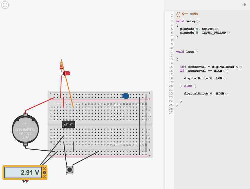
In this circuit, when the button is pushed, the LED turns off.
Reasons Behind the Circuit Design:
- Capacitor between VCC and Ground serves as a low-pass filter (filters out high frequencies) because the impedance of a capacitor is inversely proportional to frequency. So, the impedance of a capacitor for a high frequency will be low and high frequencies will pass right through from VCC to ground. -330 ohm Resistor is to prevent frying the LED. The required forward voltage for this LED was unknown, so I played it safe and viewed previous circuits we have dealt with and settled on 330 Ohms
Code
Use the three backticks to separate code.
// C++ code
//
void setup()
{
  pinMode(0, OUTPUT);
  pinMode(1, INPUT_PULLUP);
}


void loop()

{

  int sensorVal = digitalRead(5);
  if (sensorVal == HIGH) {

    digitalWrite(0, LOW);

  } else {

    digitalWrite(0, HIGH);

  }
}
KiCAD
I tried to draw the 412 circuit from memory to ensure I understood everything but clearly I didn’t understand everything. When I drew the above circuit in KiCAD, this was the result (or at least I thought):
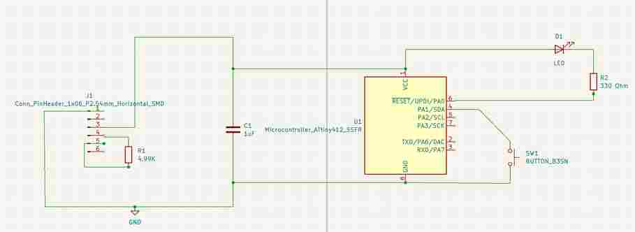
However, since the UPDI pin is being used as the digital output pin and there is nothing connected to the TX and RX pins (the 4.9K resistor placement is incorrect). The design below connects the TX/RX pins so that they can talk to eachother and uses the UPDI pin so that this board can be programmed:
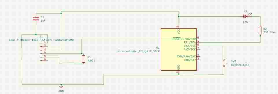
Then in the code, 0 and 1 should be changed to 1 and 2, respectively.
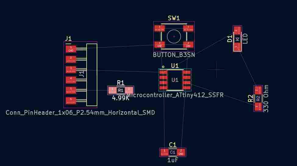
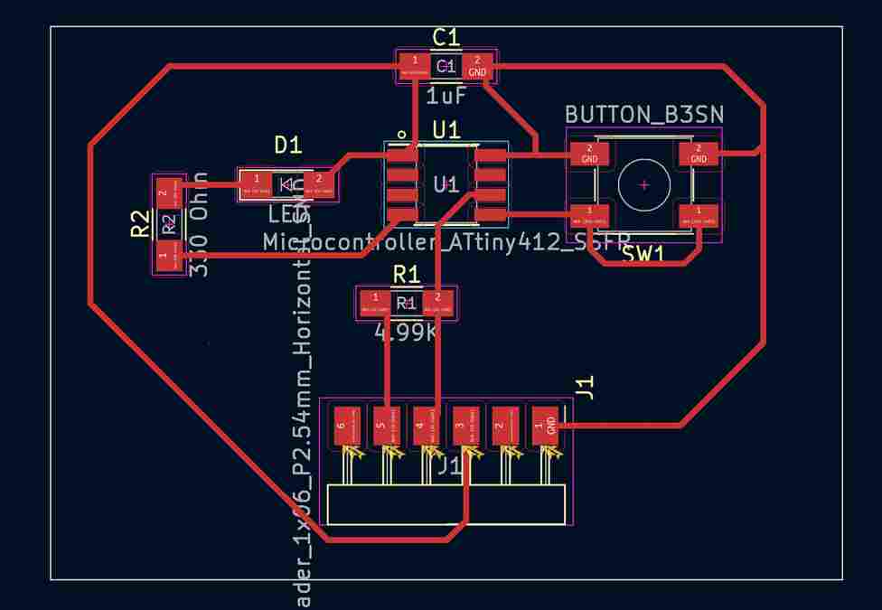
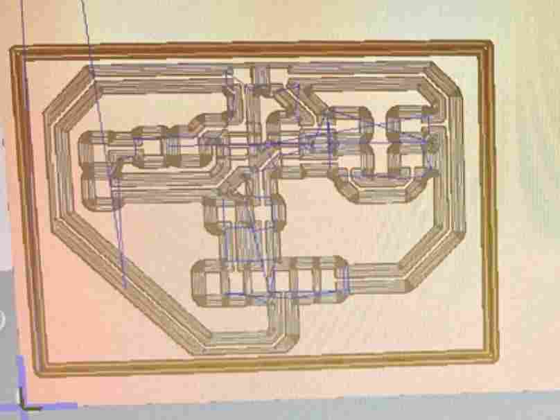
And then began editing in the pcb editor for this circuit:
After connecting the components, I checked to make sure that all design rules were met but I received this error:
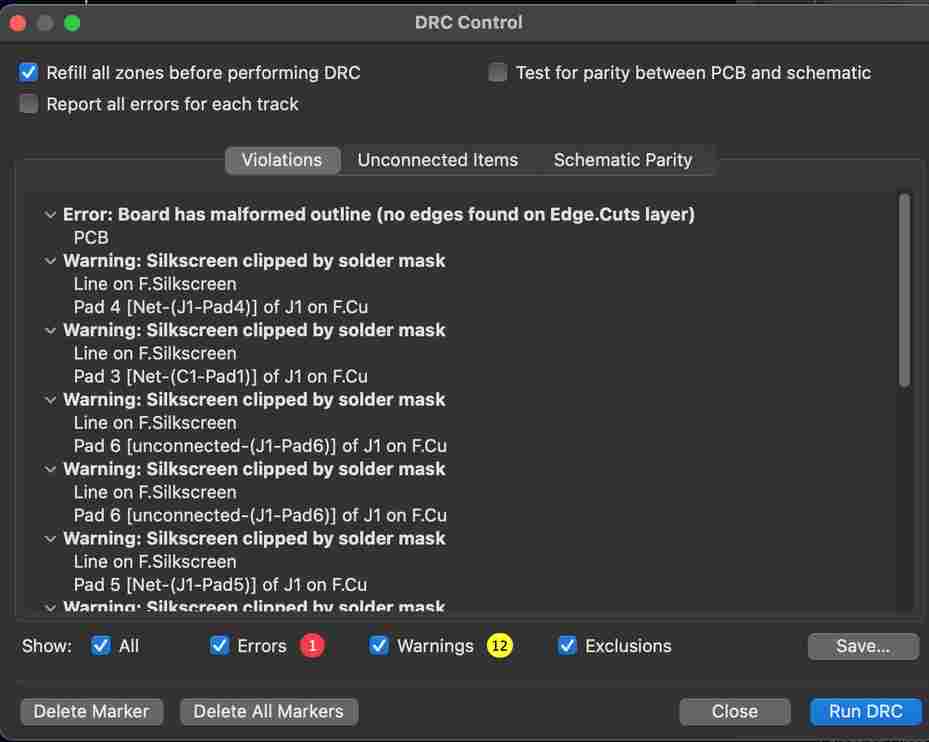
Oh no! I forgot to outline my circuit! So once I did:
I only received warnings, no errors.
When I wanted to export this KiCad file to open it up in Bantam, I used the plot function. However, at first I had these settings incorrectly checked:
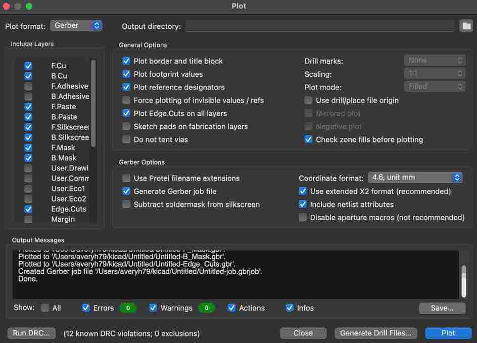
Not only did this create a million unnecessary files, but it also caused the circuit to open incorrectly in Bantam :( I forgot to get a picture, but these settings caused the entire KiCad screen (beyond the border of my circuit) to open up in Bantam - so Bantam thought the actual cut was way bigger than the size of the Mill bed. Once I changed the settings to these:
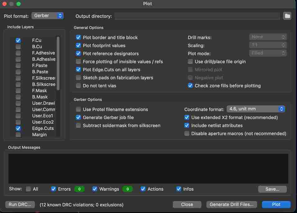
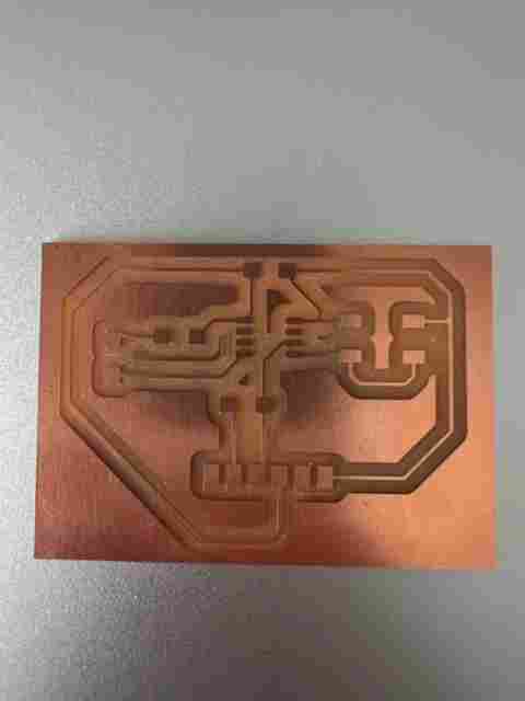
the circuit imported into Bantam Properly:
and 0.2mm trace depth and 1.5 mm trace clearence with a 1/64th and a 1/32 flat end bit, the mill cut this!
Soldering the Board
The final board is shown below:
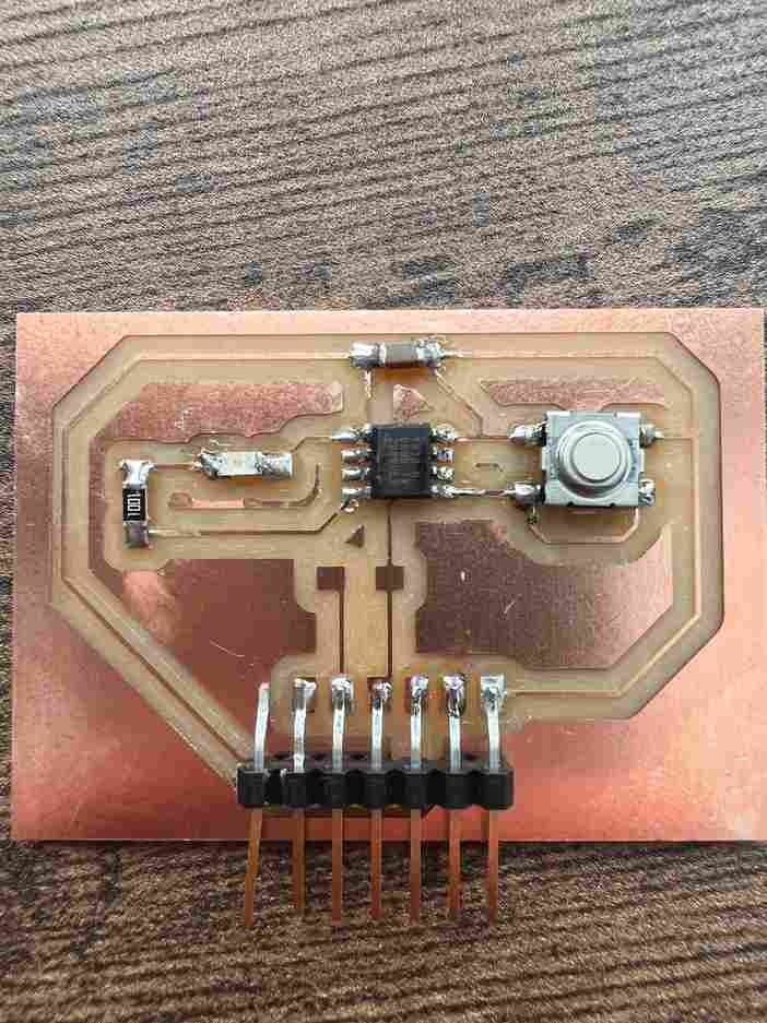
I forgot to bring home a 4.9K resistor, so I decided to upload code to the board through UPDI as opposed to FTDI. I also ended up using a 1K resistor as opposed to 330 Ohm - the LED will be dimmer but I wanted to make sure I wouldn’t fry it.
Programming Board
I followed the exact same process that I detailed in the electronics production assignment for uploading code to the 412.
The code used for this is shown below:
void setup()
{
  pinMode(2, OUTPUT);
}


void loop()

{

  int sensorVal = digitalRead(3);
  if (sensorVal == HIGH) {

    digitalWrite(2, LOW);

  } else {

    digitalWrite(2, HIGH);

  }
}
My main problem was that I forgot I had to use the Arduino’s pin 6 to program my board via UPDI. Other than that the process went very smoothly and below is a video showing the board functioning: