7. Electronics design
This week I worked on electronics design. The assignments are below :
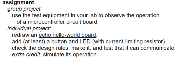
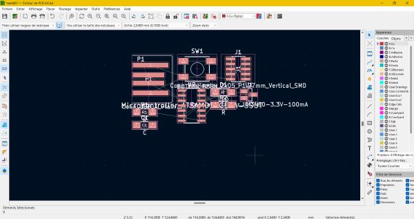
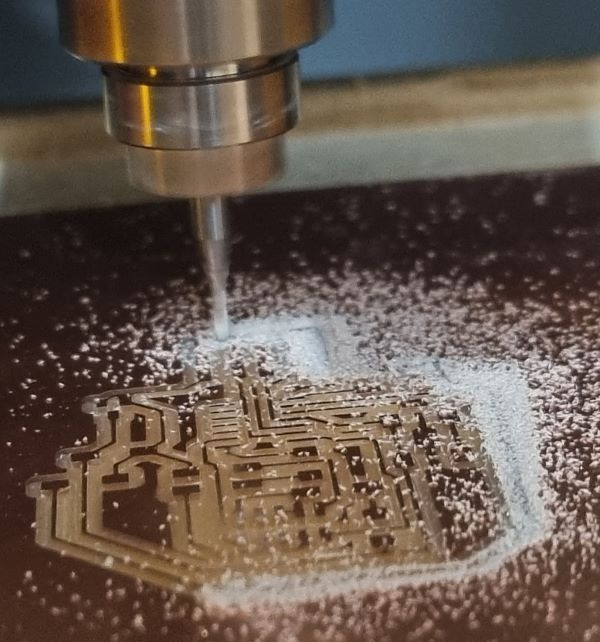
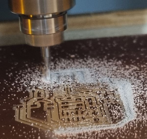
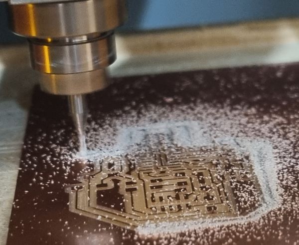
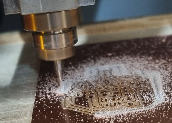
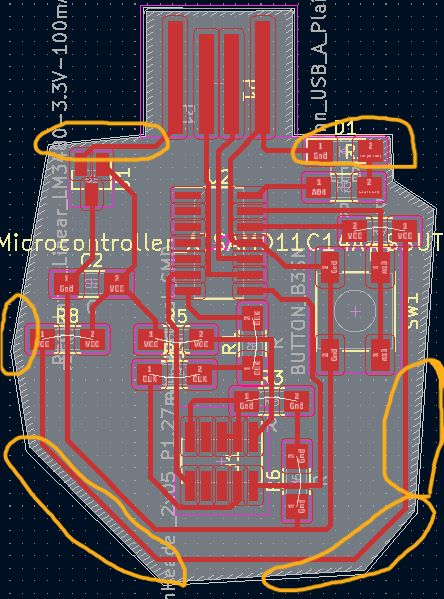
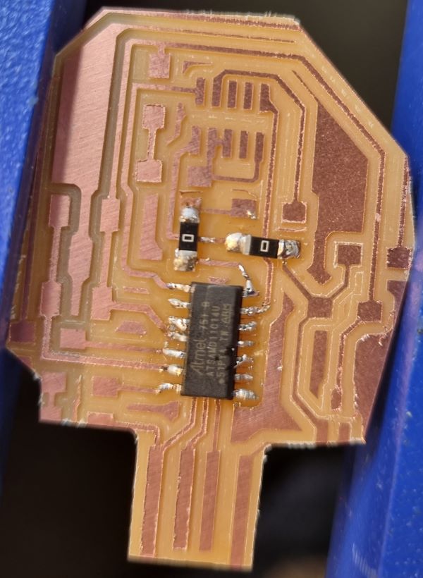
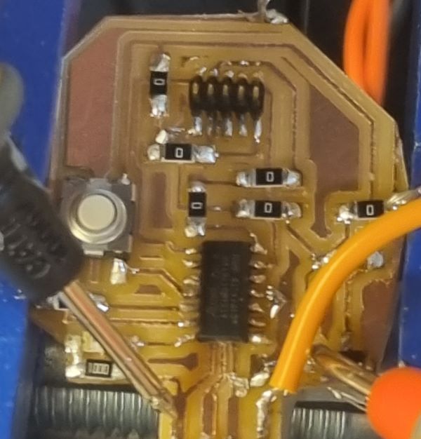
Hero shot
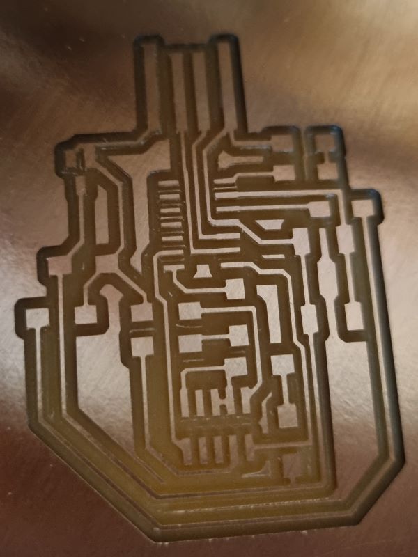
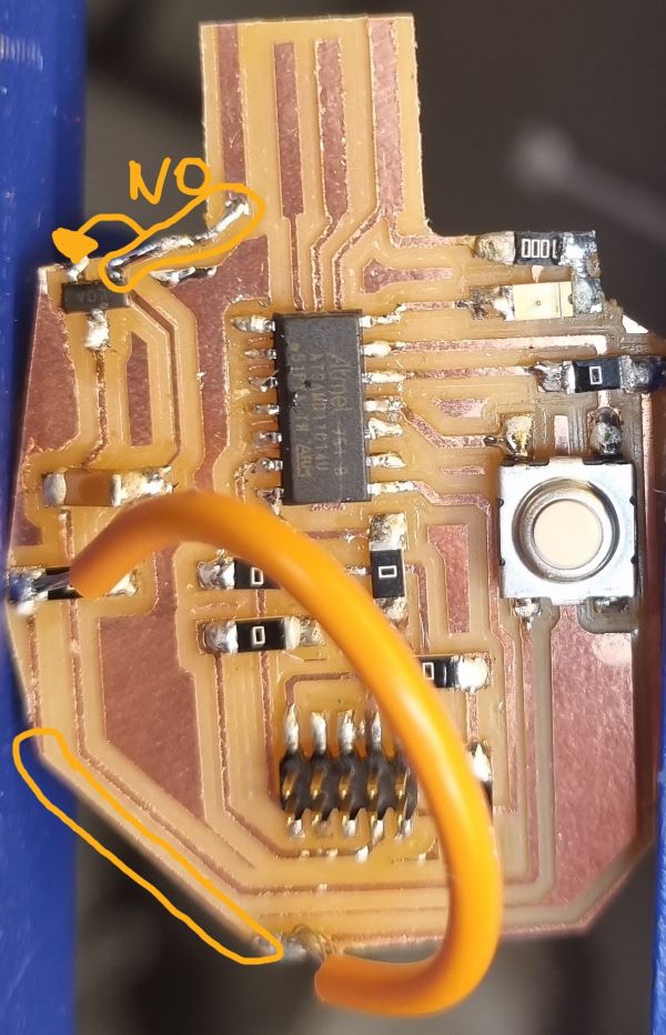
Unfortunately, these pictures contain a major mistake wich is that the 2 pins of the regulator are connected whereas they should not… It’s due to the distance between the traces wich is too small regarding the mill diameter.
Here is a current picture after removing the connecting trace with a scalpel and soldering a wire to create the good connection. (Don’t consider the 2 wires I added to have more connections some weeks later)
Designing a PCB
Kicad
First, download Kicad :
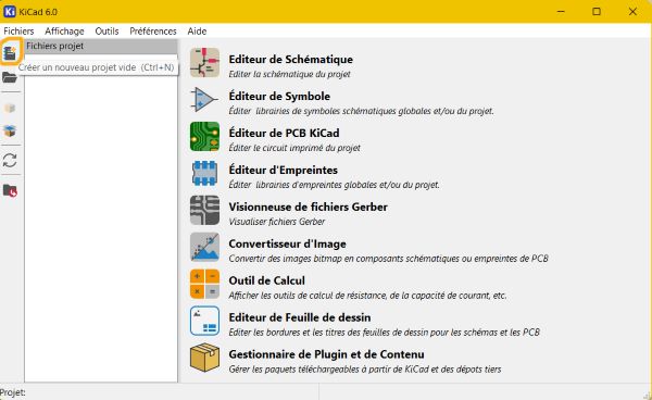
Create a project :
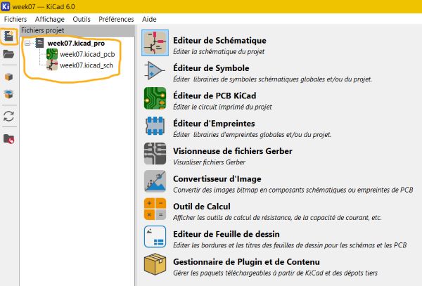
Now you have 2 files : a “.kicad_pcb” file for the PCB design and a “.kicad_sch” for the schematic
The next step is to import the fabacademy libraries :
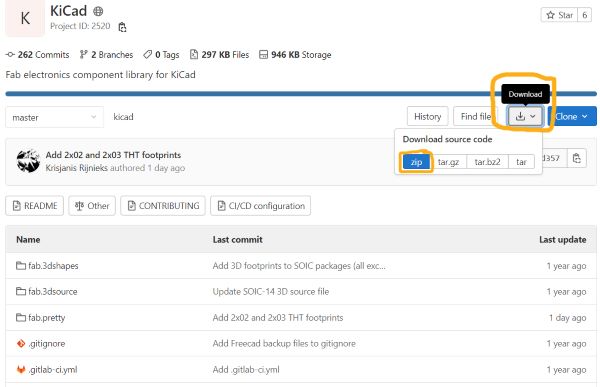
- First go to Gitlab Kicad Fabcloud :
- Download all the files :
- Then follow the installation steps :
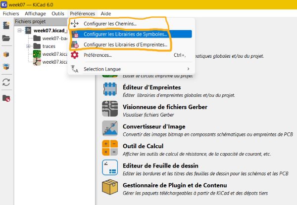
- Go to “Preferences”
- Configure the paths :
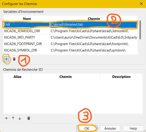
- Click on “+” to add a variable
- Call it “FAB” and point to the fab library installed on your computer
-
Click on ” Ok”
-
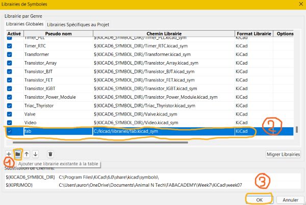
Configure the symbol library:
- And then do it for the print library
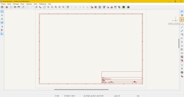
Once it’s done, you can click on your schematic file to start designing ! It opens a new page where you can add all your electronics components :
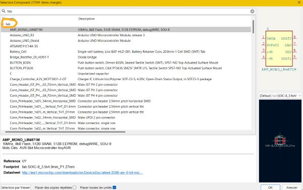
- Click on “A” for a symbol and then choose the fab library that you just import :
- When you have imported all the components you wanted, you can put some labels on the components extremities to indicate where the connexions are :
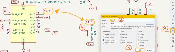
- Click on “Ctrl” + “L”
- Name the extremity
- Validate it
- Place it on your components
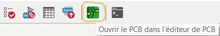
Now, you can go to the PCB editor mode by clicking on “open the pcb in the pcb editor” :
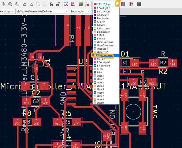
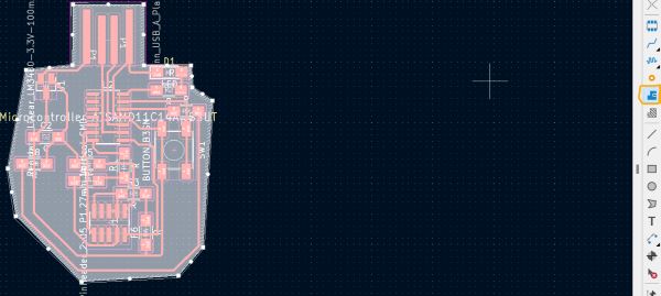
All your components are mixed… You have to find a good layout to make your traces and not put to many resistors :
The next step is to put the traces but before you have to set its diameter regarding your milling tools. In my case, I chose an internal trace of 0.4mm and an external trace of 1mm.
To set it up you have to follow these steps :
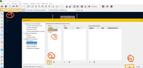
- Click on track width
- Click on “+” to add a new dimension
- Choose the dimension
- Validate it !
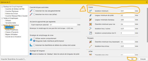
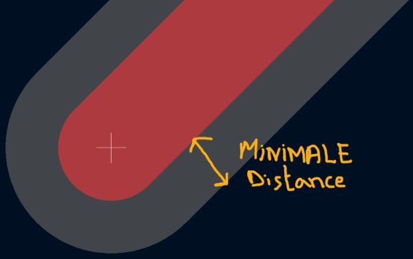
Then, you have to set some contraints to make sure traces are not too close and that the mill can go between two traces. The internal mill I choose is 0.4mm thus I chose a 0.41mm minimale isolation between two traces.
Then, you can connect all your components and add some resistors if required.
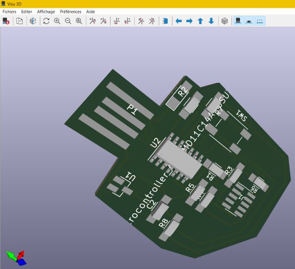
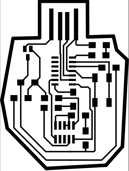
3D visu of your board :
Here are the steps to create your 3D visu :
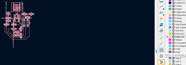
- Select “Edge.Cuts”
- Click on “Polygon”
- Click on “Alt” + “3” to make the 3D view :
Export your board :
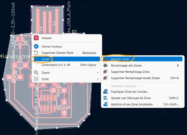
- Click on “User.1”
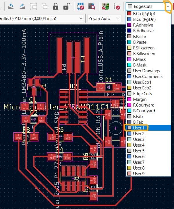
- Click on “Add a Zone” and design the outline of your board. Double click on your first point to validate it.
- Make a right click on the form and select “zone” > “fill the zone”
- Click on “File” > “Export” > “SVG”
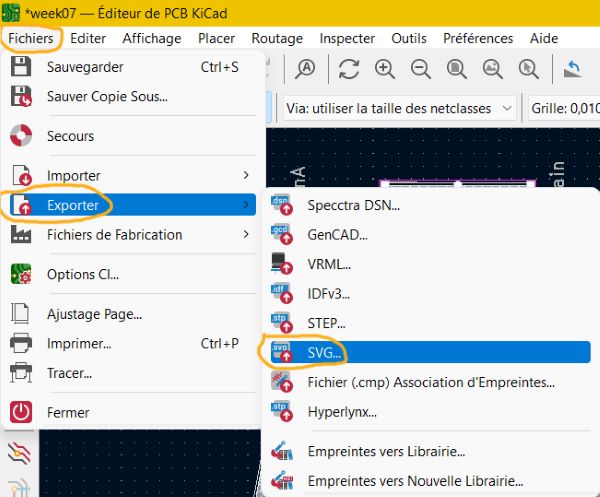
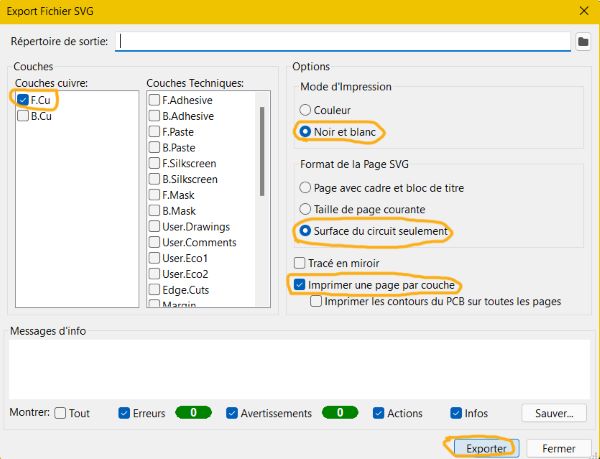
- Then export :
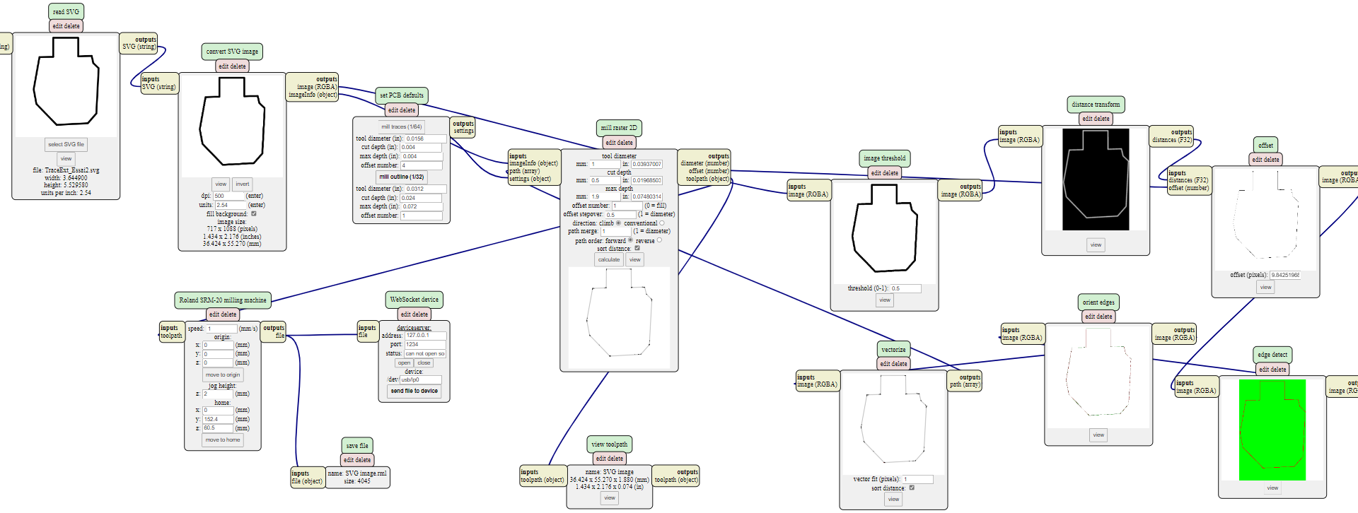
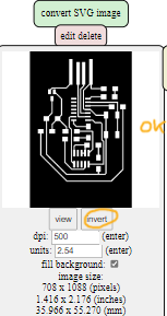
Finally you can go to Mods :
- Open Mods
- Import your SVG file
- I chose the Roland SRM 20 milling machine
- Set your parameters :
Outline parameters :
| Speed (mm/s) | Mill diameter (mm) | Cut depth (mm) | Max depth (mm) |
|---|---|---|---|
| 1 | 1 | 0.2 | 1.9 |
Trace parameters :
| Speed (mm/s) | Mill diameter (mm) | Cut depth (mm) | Max depth (mm) |
|---|---|---|---|
| 0.8 | 0.4 | 0.08 | 0.08 |
- Save it and a “.rml” file is automaticaly created for the outline and the traces
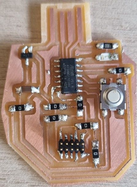
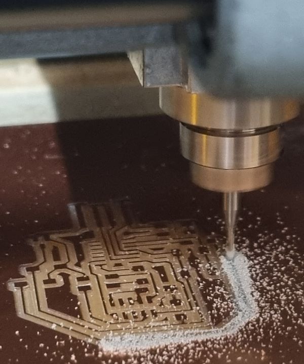
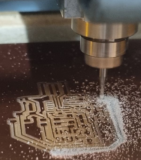
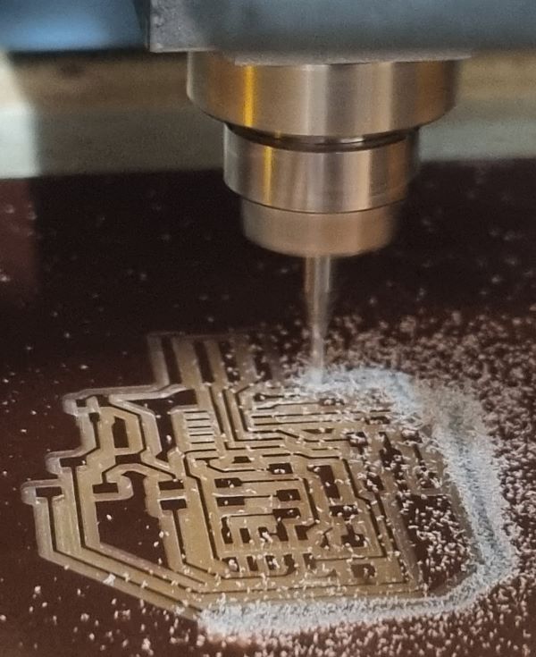
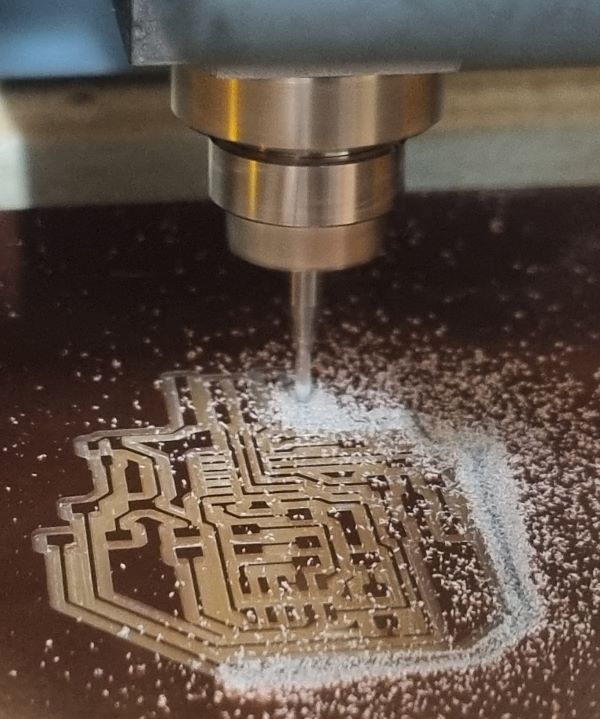
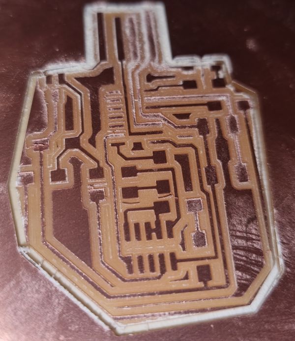
That’s the internal milling trace :
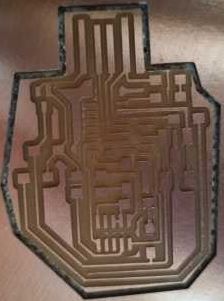
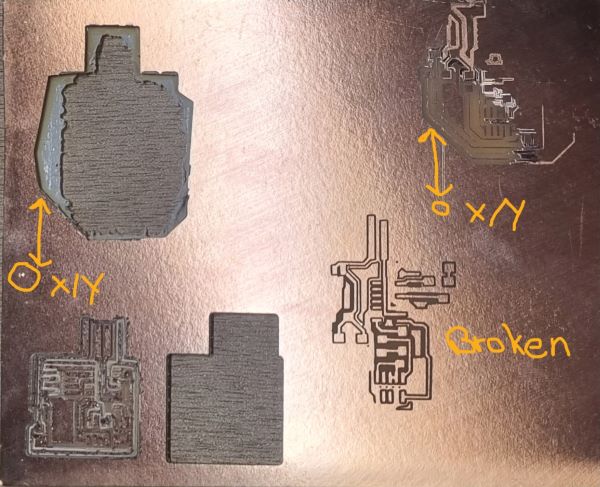
Unfortunately, the outline of the board destroyed some internal trace with my first trial :

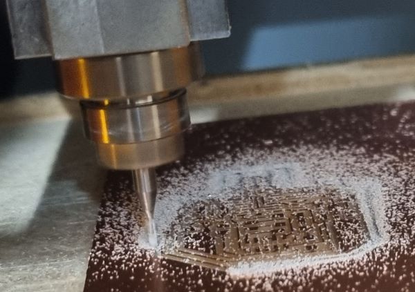
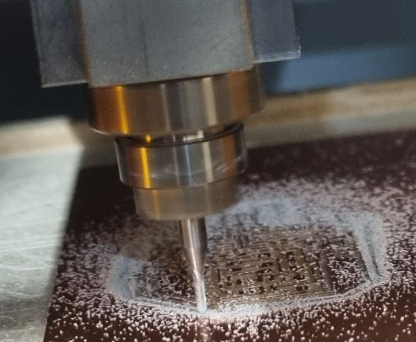
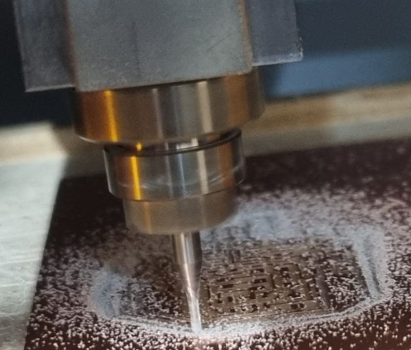
I thought it was because of my mods parameters but after a second try on another board with different parameters, the same issue appeared. So, I think it may be because of my Kicad Design :
I think I designed the outline too close from the trace.
Thus, I decide to look at my KiCad PCB file to see what I could do to improve it:
- Click on your “Cutting Edge” line
- Click on “Properties” and put a 1mm line diamete
- Then move your “Cutting Edge” line to increase the distance with your traces
- Export the “Cutting Edge” only to SVG file
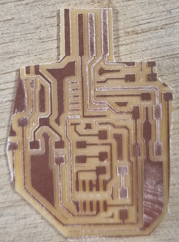
- Check if it fits well with your internal traces on Inkscape :
And then I put it on mods and folllowed the procedure explained below :
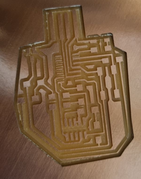
That’s the final result :
Soldering your components
- Start by the smaller and internal component that will be difficult to access
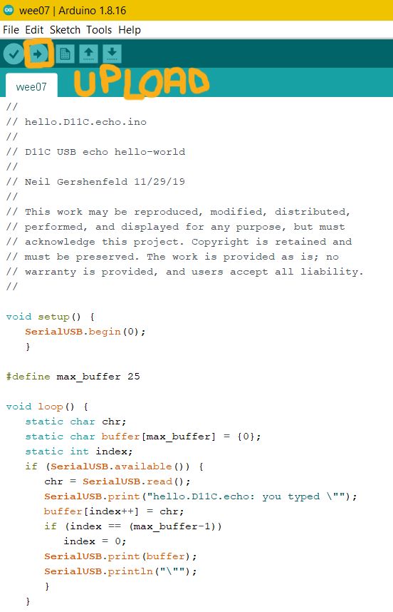
Flashing your board
If you’re using an ATSAMD11C microcontroller you can follow these steps as well as these instructions
- Download that Hello world File in the same folder where you put the EDBG file
- Open it with the Arduino IDE that you have to download.
- Follow the steps of that 35 seconds Instruction Video
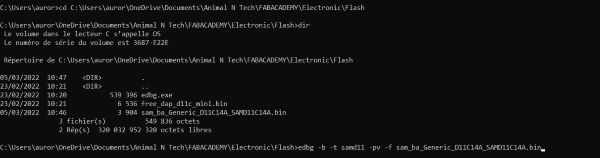
- Open your computer invite and write this line :
edbg -b -t samd11 -pv -f sam_ba_Generic_D11C14A_SAMD11C14A.bin
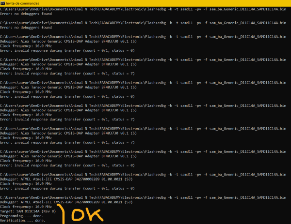
- Connect your board with the programmer you did before (or with another working programmer) and connect it to your computer with the USB port
- Select the correct port on Arduino IDE where your programmer is plugged
- Click on enter on your computer invite and your board should be flashed ! I had some bad contacts issues, I first used my programmer and then I used the Atmel ICE programmer and it works :
- Now disconnect your programmer and set the arduino IDE parameters :
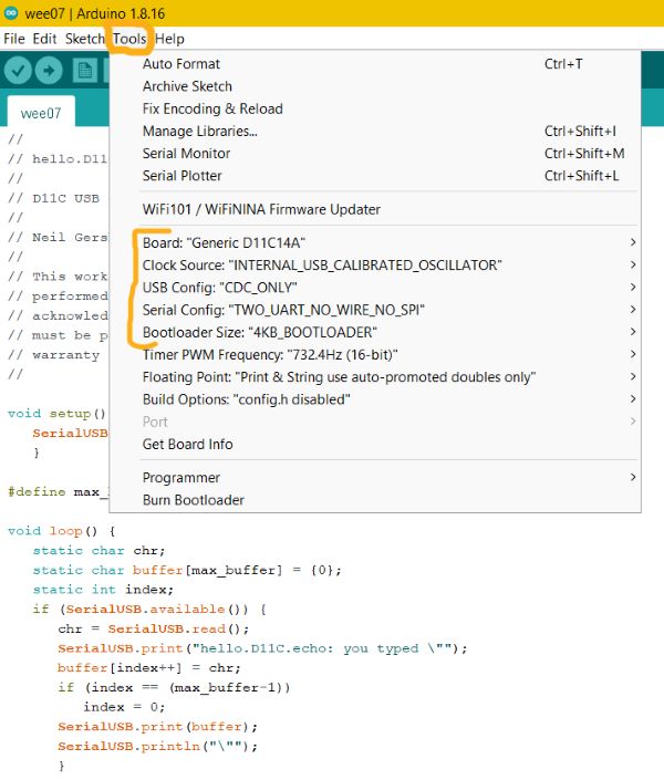
- Go to your Arduino IDE and click on “Upload”
- Finally click on “Serial Monitor” by clicking on “Ctrl” + “Shift” + “M” and you should see the hello world message !
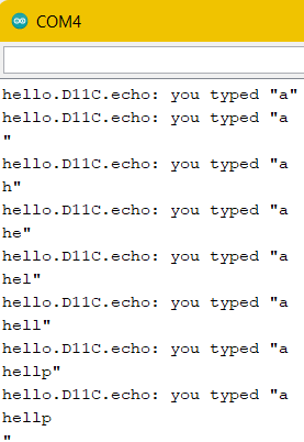
I also had some bad contact messages…
Group assignment with Luc Hanneuse from Agrilab
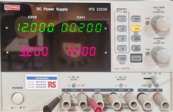
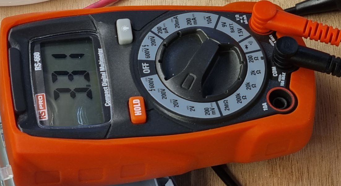
We measured the power on the board with different tools to see if the electrical circuit is working :
- RS Pro DC Power supply IPS 3303S at 5V :
Mistakes
- Kicad : parameter the trace isolation parameters and diameters. Distance between the outline trace and the internal trace.
- Mods : put the interior in white and the exterior in black by clicking on the “invert” button or you could have an offset.
- Milling machine : broken mills, bad X/Y settings
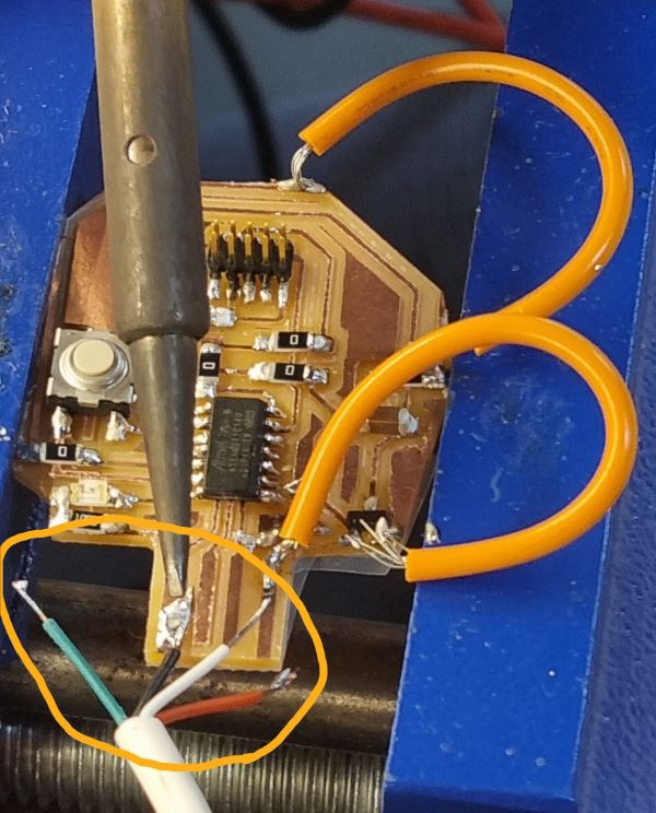
- soldering : I soldered on the USB port and so it wasn’t working anymore. We had to solder an USB port to make it works
Files
Useful links
- Kicad
- Gitlab Kicad Fabcloud
- Mods
- instructions
- Hello world File
- EDBG file
- Arduino IDE
- Instruction Video
- RS Pro DC Power supply
- RS Pro compact digital multimeter