6. Electronics Design
I. Group Assignment
II. Individual Assignment - Designing my own PCB
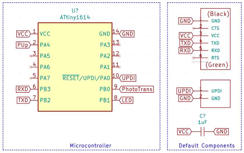
I aimed to design a board around an ATtiny 1614 that would contain the following four elements:
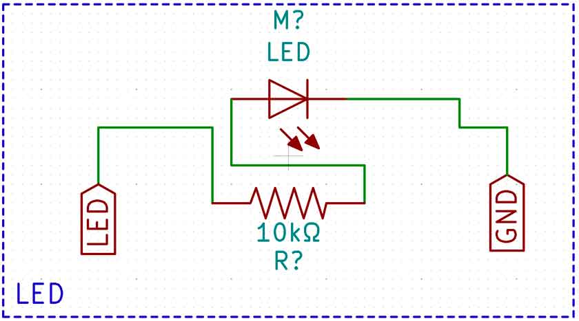
- A programmable LED
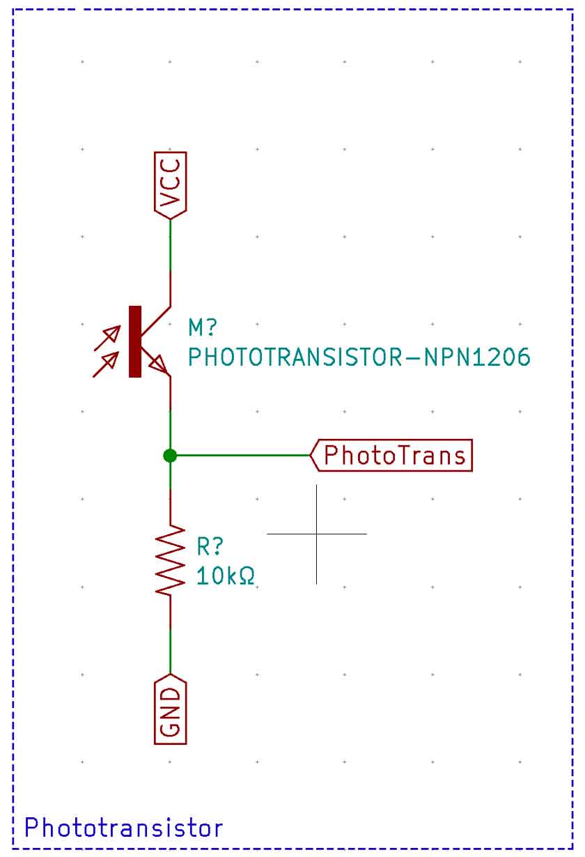
- A phototransistor
- A Switch button
- Some sort of logic gate
A. Sketching the circuits
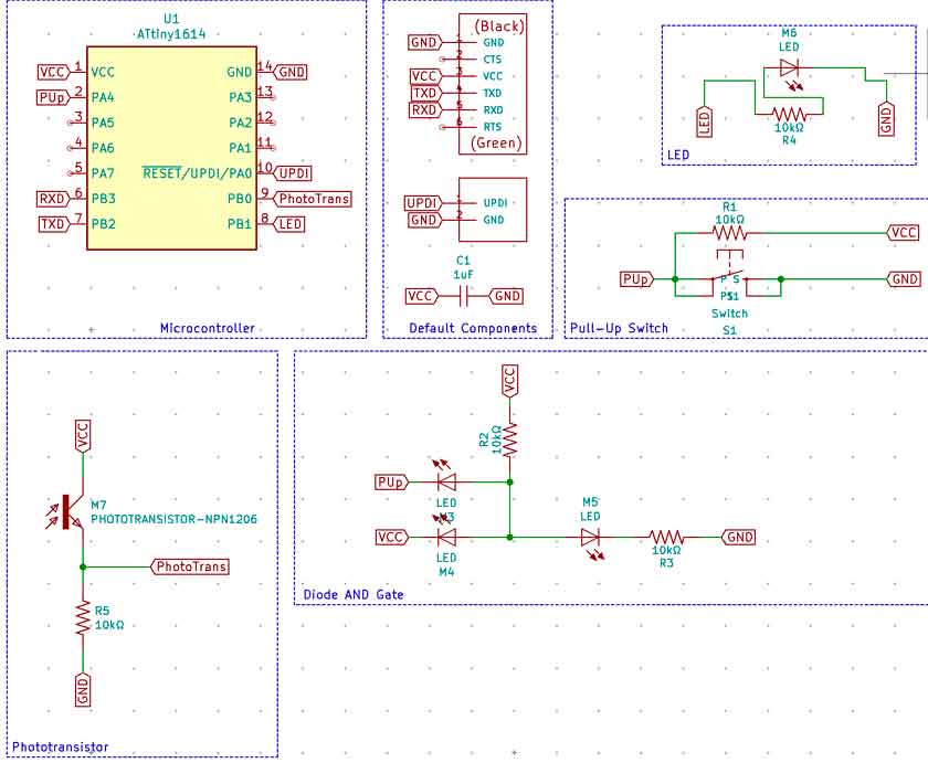
On Kicad’s Eschema module, I first placed and linked the Central components (Microprocessor, FTDI, UPDI and 10uF Capacitor)
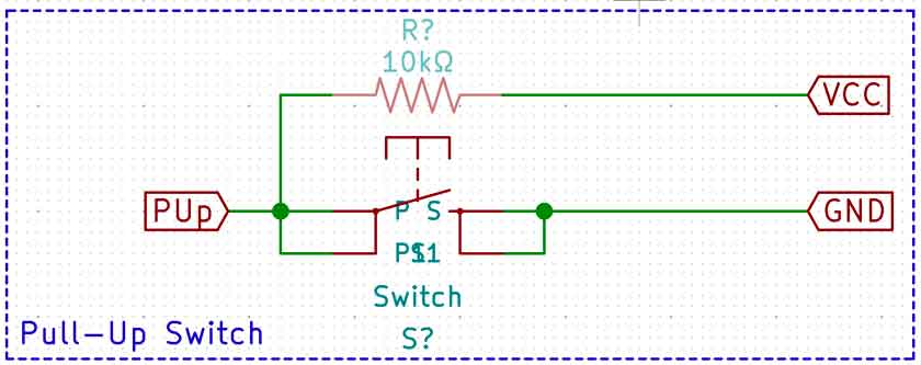
I then added circuits for an programmable LED, a phototransistor and a pull up Switch
Logic gates perform logical operations on one or more binary inputs, producing a single binary output. In other terms, logic gates can be used to impose conditions on the flow of current through a circuit. The 7 categories of logic gates are described below where True indicates a potential difference greater than 0.7V, and False, a potential difference smaller than 0.7V.
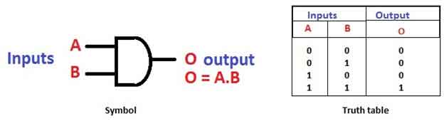
The output of this gate is true only when all the inputs are true. When one or more inputs of the AND gate’s inputs are false, then the output of the AND gate is false.
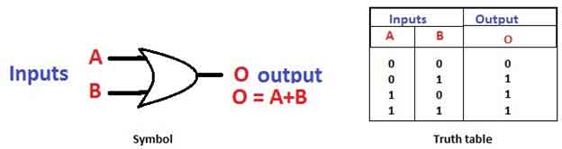
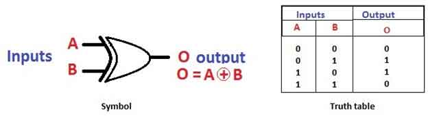
The output of the OR gate is true only when one or more inputs are true. If all the i/ps of the gate are false, then only the output of the OR gate is false. The symbol and truth table of an OR gate with two inputs is shown below.

The output of the NOT gate is the reverse of the input. When the input of the NOT gate is true then the output will be false and vice versa. The symbol and truth table of a NOT gate with one input is shown below. By using this gate, we can implement NOR and NAND gates
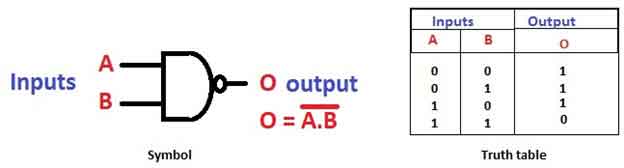
The NAND gate is designed by combining the AND and NOT gates. If the input of the NAND gate high, then the output of the gate will be low.The symbol and truth table of the NAND gate with two inputs is shown below.

The NOR gate is designed by combining the OR and NOT gate. When any one of the i/ps of the NOR gate is true, then the output of the NOR gate will be false. The symbol and truth table of the NOR gate with the truth table is shown below.
If any one of the inputs of this gate is high, then the output of the EX-OR gate will be high. The symbol and truth table of the EX-OR are shown below.
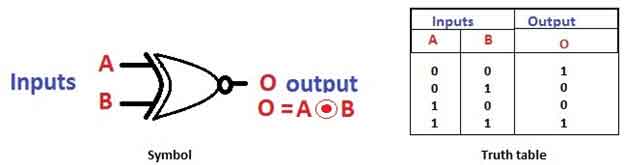
When both the inputs of this gate are high, then the output of the EX-NOR gate will be high. But, if any one of the inputs is high (but not both), then the output will be low. The symbol and truth table of the EX-NOR are shown below.
Transistors are commonly used as central components in logic gate circuits as shown here. Diodes can also be used to produce AND & OR logic gates. However, compared to transistor logic (TL) gates, diode logic (DL) gates offer limited isolation between input and output. Furthermore, the amount of inputs (Fan in) and outputs (Fan out) DL gates can handle is relatively low. Nevertheless, I decided to design a DL circuit as wanted to determine its characteristics for myself.
My aim in implementing a logic gate was to test the functionality of parts of my board, namely the power delivery throughout as well as the switch.
Pull-up switches deliver a constant voltage as an output. when the switch is activated, the output voltage falls below 0.7V. As such, I have decided to use a AND DL gate. The gate would provide an output voltage greater than 0.7V should when the switch is in its neutral state and power is delivered to the board. However, should one of these conditions not be met, the output voltage would fall below 0.7V. I based my design on the following resources:
The gate is composed of three LEDs. The output LED will turn on if all conditions are TRUE. On the other hand, should one of the inputs be False, its corresponding LED will turn on and the output LED will remain off.
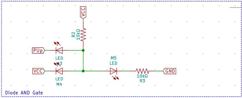
| Switch | VCC | Output |
|---|---|---|
| 0 | 0 | 0 |
| 0 | 1 | 0 |
| 1 | 0 | 0 |
| 1 | 1 | 1 |
Overview of Circuits
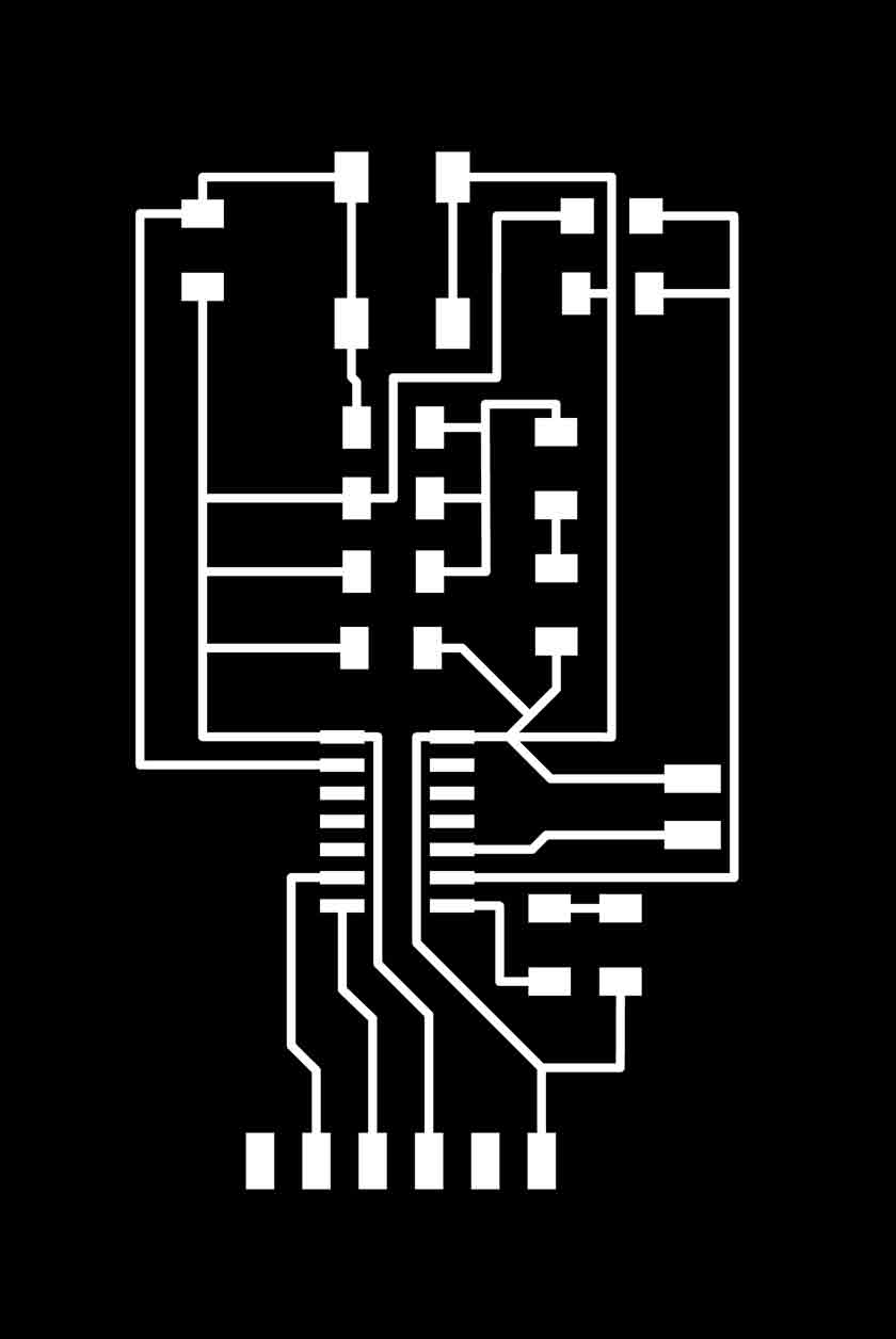
B. Designing the Board’s layout
Having completed the circuits, I then moved to placing components around the microchip. I set the track width to 0.4mm, developed multiple iterations and ended with the below.
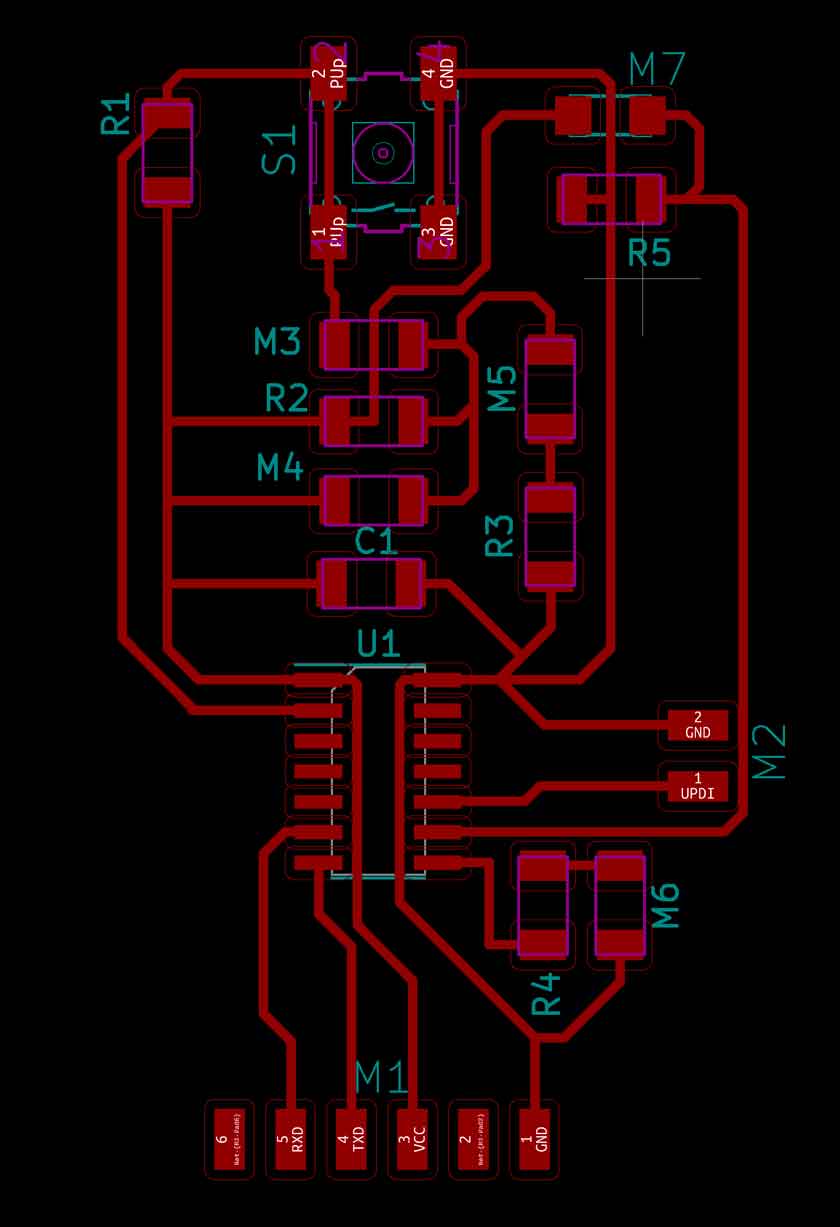
List of Components
| Reference | Component |
|---|---|
| Cx | Capacitor |
| M1 | FTDI |
| M2 | UPDI |
| M3 | DLG LED 1 (Input = Switch) |
| M4 | DLG LED 2 (Input = Power Source) |
| M5 | DLG Output LED |
| M6 | Programmable LED |
| M7 | Phototransistor |
| S1 | PullUp Switch |
| Rx | Resistor (See circuit) |
| U1 | ATtiny1614 Microchip |
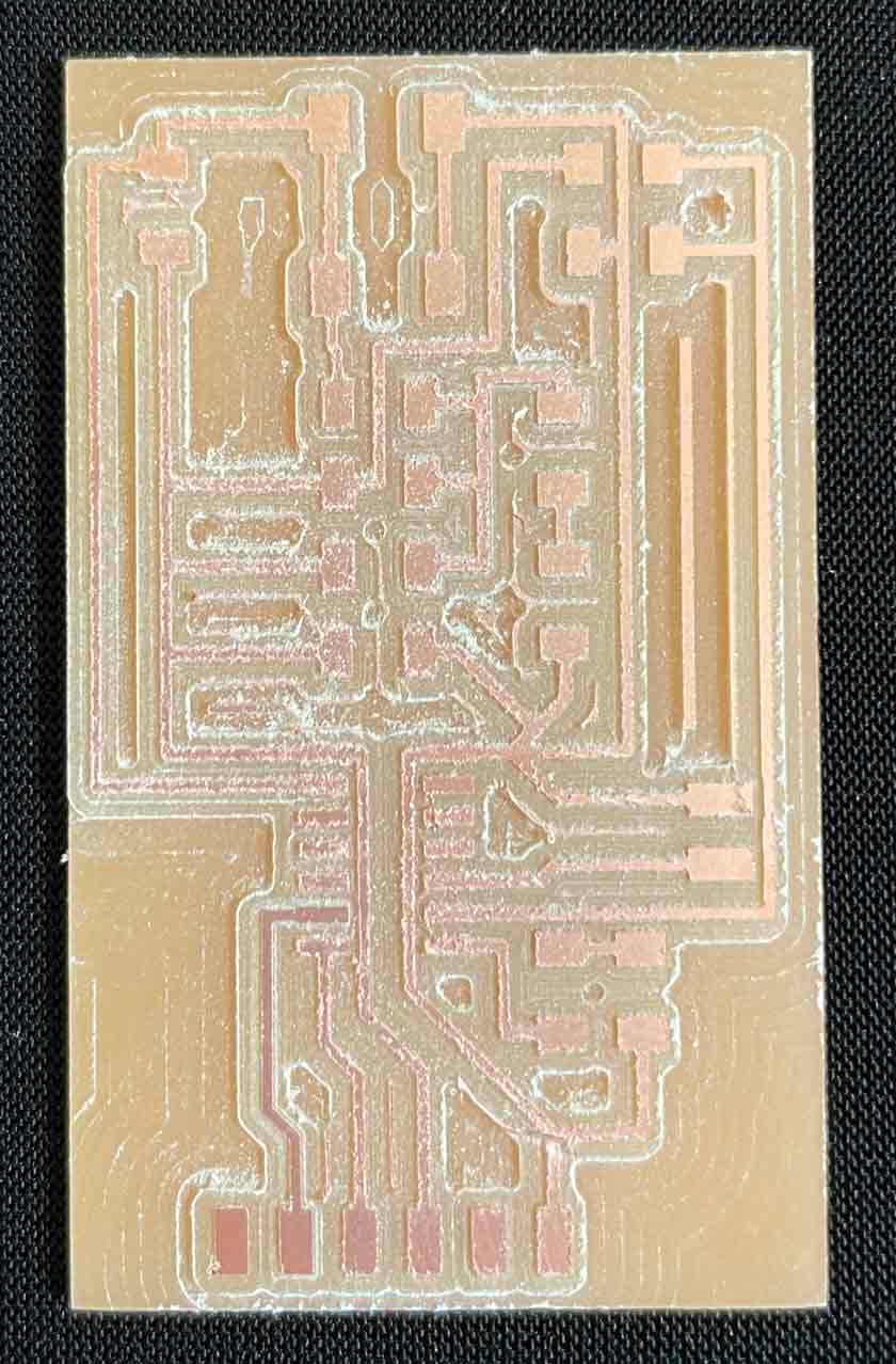
C. Milling the Board
Trace milling was setup in climb mode.
Broken end-mill
My 1/64 end-mill broke while it was milling the traces. The board was therefore incomplete.
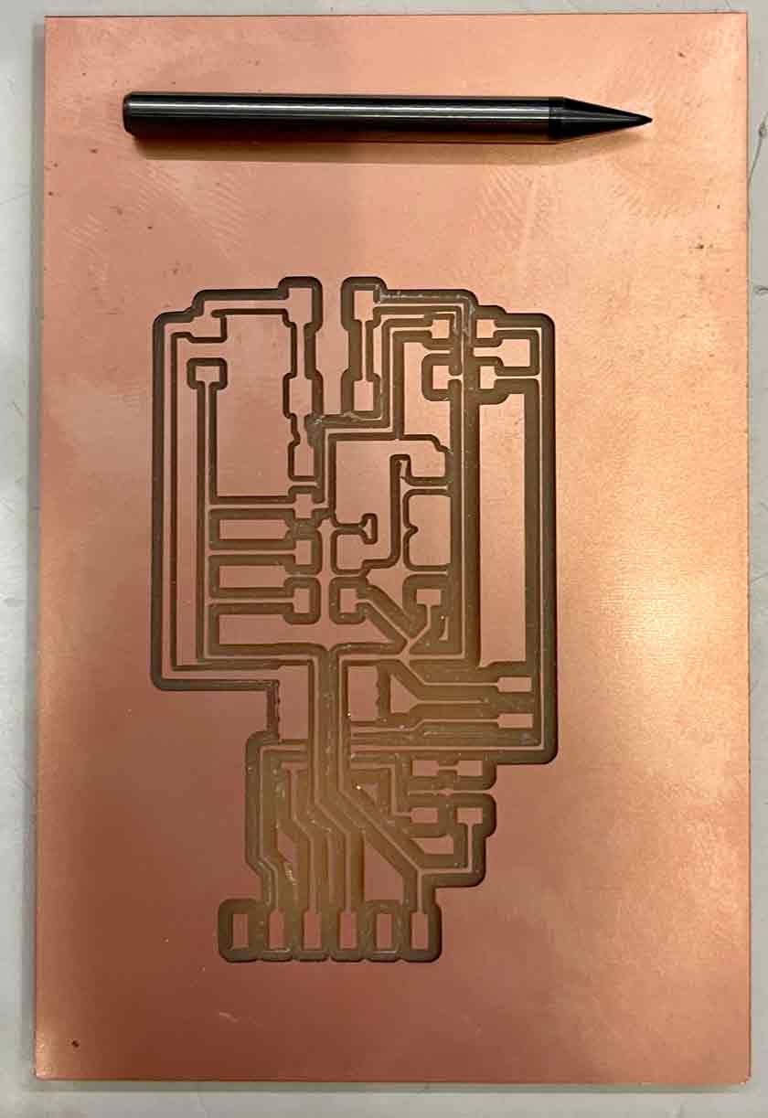
I obtained a new one and started over. The second try worked perfectly (No pictures sadly).
I attempted to use the 1/32 end-mill to remove all unecessary copper within the board. To do so, I prepared a cut file on mods which used the parameters listed in the below table. As suggested by Diego Diaz
| Parameter | Value |
|---|---|
| end-mill | 1/32 |
| cut depth | 0.004 |
| max cut depth | 0.004 |
| offset number | 0 (fill) |
| offset step-over | 0.9 |
| speed | 4 mm/s |

Ensure Z-axis zero and cut paramters are properly set before milling excess copper
For some reason, the end-mill seems to have sunk into the board when I was testing the zero point I had set. I didn’t notice it at the time. However, the traces it made were much deeper than those previously made. I believe this could be due to the fact that I had used the same X/Y coordinate as for the 1/64 mill to set that of the 1/32. That point must have been slightly lower than the surface of the board du to the presence of a surface hole I had made to ensure the 1/64 mill was in-fact touching the board’s surface.
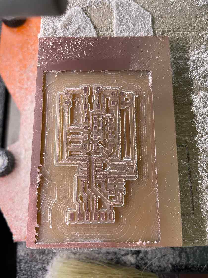
Further to this, the tracks of each passage are clearly visible. This is most probably due to the offset step-over value being too high.
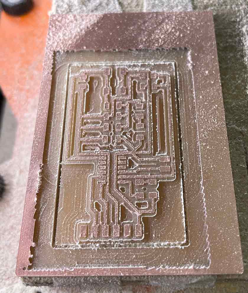
Nothing special here. I reset the zero point in the Z-axis to ensure the end-mill wouldn’t cut too deep and reach the wooden platform underneath the board.
D. Soldering Components and Testing the Board
Once the milling process had been completed, I soldered the different components onto the board.
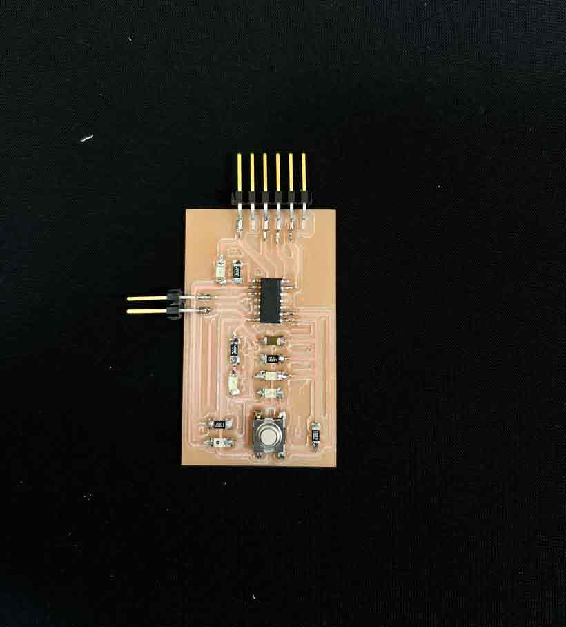
I used a multimeter to ensure all connections and paths were working as intended, which they were.
Finally, I connected the board to a computer through an FTDI board.


As shown above, the logic gate’s output LED was on, indicating that all conditions were therefore True. When the button was pressed, and the switch therefore closed, its corresponding LED would turn on, and the gate’s output LED would turn off.
However, I realised that the circuit I had designed for the gate made no sense. Should power be provided to the board or not, both the input and output of the power LED would have the same potential difference. As such the LED would remain off. Moreover, I can’t even short the circuit to light up the LED. Not very logical reasoning for a logic gate.
Nevertheless, the switch’s LED proved that it worked. In the end, it was not all for nothing.
E. Programming the board
I attempted to program the board with a simple blink LED Arduino sketch using Arduino IDE and got the below error. I researched it and found that it was probably due either to Arduino FTDI drivers clashing with existing ones on MacOS, or the USB3.0 connection Hub dongle I need to use to connect the board to my Macbook.
I therefore tried using a PC with windows installed, and it worked. It seems that I will need to use a windows pc until I figure out how to get it to work on
Appendix
###### Abbreviations and Common Terms

SMT - Surface Mount Technology

SMD - Surface Mounted Device

Through-Pin

###### Components

|Component|Function|
|-|-|
|Actuators|

Battery
Button
Capacitor (Polarized & Unpolarized)
Crystal/Resonator
Diode (Regular, Zenner, Shottky + Other?)
Inductor
MicroController
Op-Amp
Regulator
Resistor
Sensors
Switch
Transistor (bipolar/mosfet)
Wire

###### Standard units, Laws & Formulas

KCL/KVL

Power + Power across regulator

###### Common Circuits

LED

Pull Up/Down Resistor

###### Design Rules

Minimum thickness of traces and gaps