Electronics Production
2020
Sumary
This week we started learning electronics production. We are tasked with a group assignment, to characterize the design rules for your PCB production process, and an individual assignment, to make an in-circuit programmer by milling and stuffing the PCB, testing it, then optionally try other PCB processes.
Fab Lab FCT has two precision CNCs, a Shapeoko 2 and an Inventables Carvey 2. The shapeoko is losing steps in one of its axis, so it’s not really carving precisely enough to produce PCBs yet. The process of troubleshooting it is ongoing, but it has the advantage of open hardware and using GRBL, an open source firmware that is easily configurable and compatible. Once it’s mechanically reliable, it should be the best option available. The Inventables Carvey 2 can be very precise as its mechanics are robust, but as a hobbyist machine, it’s meant to be used with an online software called Easel. Easel isn’t precise enough to produce PCBs. It is important to be able to do auto-leveling, as the cut depth is so shallow and the slighted deviation can lead to no cut at all, or a cut that’s too deep, or both on the same cut job, as the material may be slanted. Easel doesn’t seem to contemplate auto-leveling.
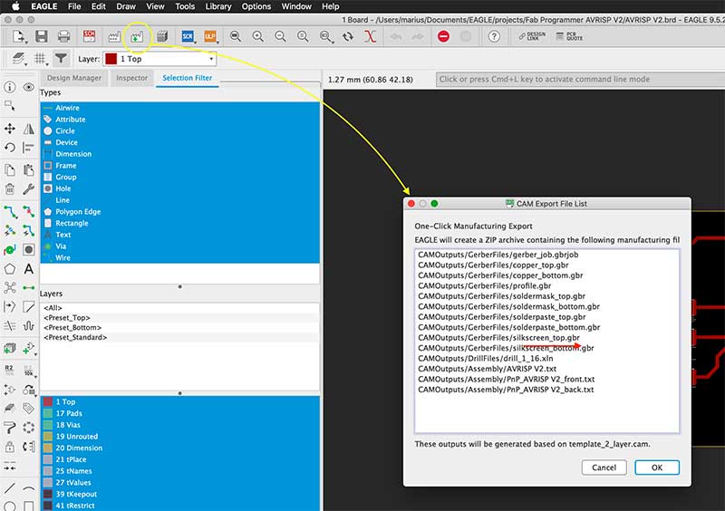
Usually the process is to create the electronics and schematics in Autodesk Eagle, then generate and export CAM data as a series of Gerber files. These are then processed in FlatCam to produce G-Code, then imported into Chilipeppr GRBL Workspace, an online GRBL parser and machine controller, which does support auto-leveling and allow for greater control of the machine. Yet, Chilipeppr doesn’t seem to work well with Carvey’s version of GRBL gCarvin, so we were kind of stuck at the beginning of this week.
One alternative we’re considering it to use the y-Cutter to create the electronic vias, and with a mask of kapton tape, protect it from the heat necessary to solder the components.
Group project: Design Rules
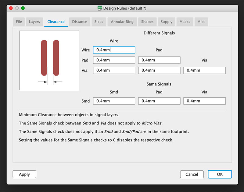
The Design rules for milling a board are conditioned by the size of the bit or “tool” used on the CNC to cut the vias, which in our case is of 0.4mm, so we set the Clearance to that value in Eagles’ design rules, leaving all other values at Default.
Individual Project
I’m producing am FabTinyStar AVR ISP based on Brian’s design, which is a one layer, milled PCB, populated solely with surface mounted components and ATtiny45.

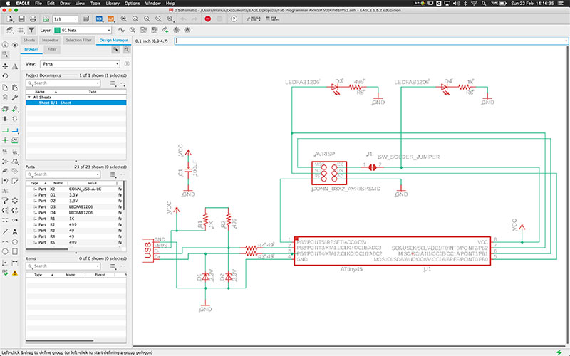
We started by getting to know the process of drawing an electronic schematic in Eagle. We first downloaded and imported a Fab component library, so we could populate our electronic project in Eagle with components that are available at FCT FabLab.
We then proceeded to list all the components needed onto the sheet, placing them so that it is easier to understand the logic of the circuit. Then the connections were made between all the components with so called airlines.
Once that part was complete, we turned to the board layout view, where all the components need to be placed in such a way as to allow them to be connected by all the vias, or “electric roads” that are then laid out between them with the Route Airwire tool. It’s a bit of a puzzle to figure out as some vias need to be routed in the available space between components. Also, the width of the vias needs to be set to the router tool width, because that width is what will be produced on the CNC. I made the mistake of forgetting that and laying out thin vias which I had to widened out later with a command “Change width” and selecting each of the vias to do it.
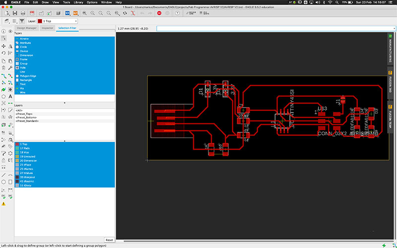
Finally, on my second attempt, the board was ready to export.
Vinyl Cutting the circuit
As out Carvey wasn’t working yet, we tried cutting the circuit on the vinyl cutter. For this we exported the board schematic from Eagle as a PNG file
This was then converted to a vector file in Inkscape using the trace bitmap command, followed by Object to Path. A bit of cleanup is needed to remove some double traces, and after that the vector file can be sent to the Vinyl Cutter. A length of copper tape was laid out on top of a piece of leftover vinyl we had around and aligned in the Vinyl Cutter.
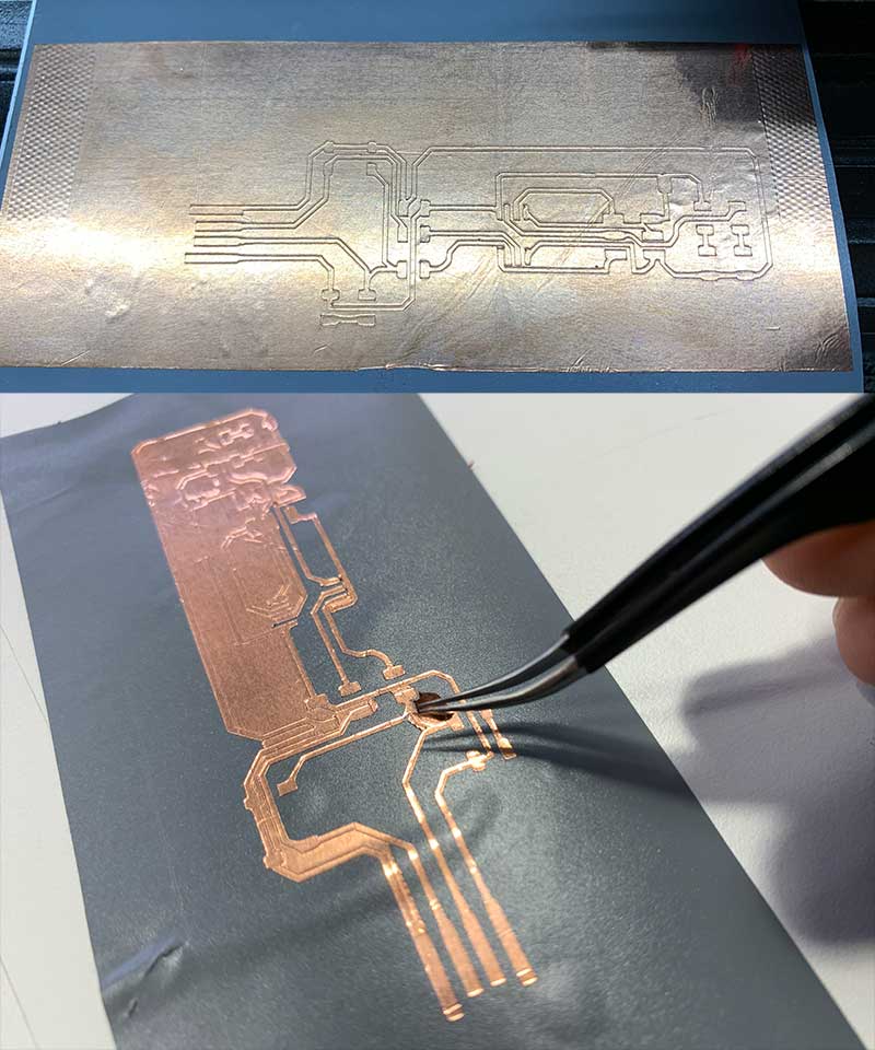
At this point I removed most of the excess copper, but botched some via. I could have restarted the cut, but it was apparent that the process is finicky and yields a fragile circuit for my unpracticed hands to work on, so I decided to quit and move on to the milling process, as that was working by then.
CNC Milling the Board
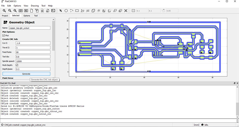
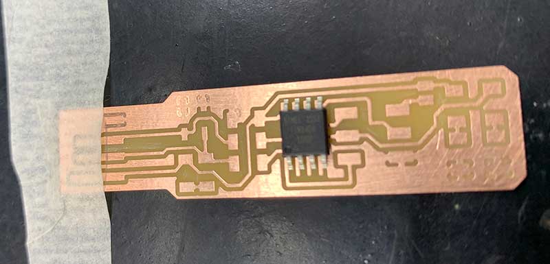
The Gerber files include each layer in the Eagle board schematic as separate files, but in my case only the Copper Top, for isolation milling, and Profile, for cutting the boards shape, were relevant.
These Gerber files were imported into FlatCam, where many parameters are set for each file:
For isolation milling these were the values set, which were tested by our Fab Manager and confirmed to be good.
- units are set to mm (because reasons - international standards and all - our bits are measured in mm)
- tool diameter = 0.2mm (out smallest end mill)
- width, or number of passes = 3 (we could increase this value to remove more copper, but it’d take longer to mill and the vias wouldn’t be any more isolated)
- pass overlap = 0.1mm (half the mill width, to make sure)
- Cut Z = -0.065 (so as to go through the the copper layer of the board but not so deep that we’d have to reduce the feed rate to preserve the mill bit)
- Travel Z = 2 (lift value when traveling to another part of the milling job so as not to interfere with copper burr on the board)
- Feed Rate = 100mm/m (milling speed during x & y movements)
- Spindle Speed = 12000 rpm (rate at which the spindle turns)
Press Generate and Flatcam generates the paths for the endmill
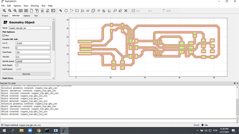
It’s important to verify that all the vias are separated from each other by examining the paths carefully.
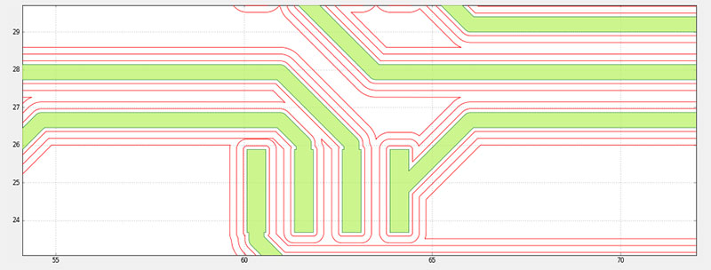
If satisfied, the paths can be exported as GRBL files.
For the Cutout, the process is the same, but the parameters change according to the necessary cut (in this case the rectangular shape around the circuit)
- Cut Z = -1.9mm (to actually go through the board)
- Travel Z = 1mm (not a complicated shape, won’t actually need this much)
- Feed rate = 80mm/m (slower than before because we’ll be plunging more into the material)
- Tood Diameter = 0.8mm (this tool is stronger and can plunge deeper into the material without as much risk of bending or breaking)
- Spindle Speed = 12000 rpm (same rotational speed as before)
- Muti-depth = on or checked (as we’re repeating the pass at different depths)
- Depth per Pass = 0.3mm (depth of each pass)
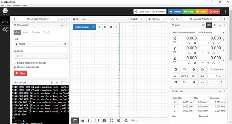
In out case, we still resort to another piece of software called CNCjs, which controls the CNC, to move the spindle to where we want Zero to be, Zero out those coordinates, then turn Carvey off (or use the reset button that was being developed at the time as a modification for this purpose by out Fab Manager) and turn it back on again, make sure Carvey reports the current coordinates as 0X 0Y 0Z. CNCjs doesn’t natively do auto-level, which is crucial for PCB isolation milling, so we then resort to ChilliPeppr for that and the milling.
The GRBL files are imported into ChilliPeppr, a Java WebBased Application that controls the Inventables Carvey 2 CNC through a serial port JSON Server connection that needs to be previously started, just like CNCjs. We make sure the connection is active and proceed with the auto-leveling of the are we need to mill. Once that is over, the values are applied to the original gcode. After confirmation by analyzing the gcode, the milling can proceed.
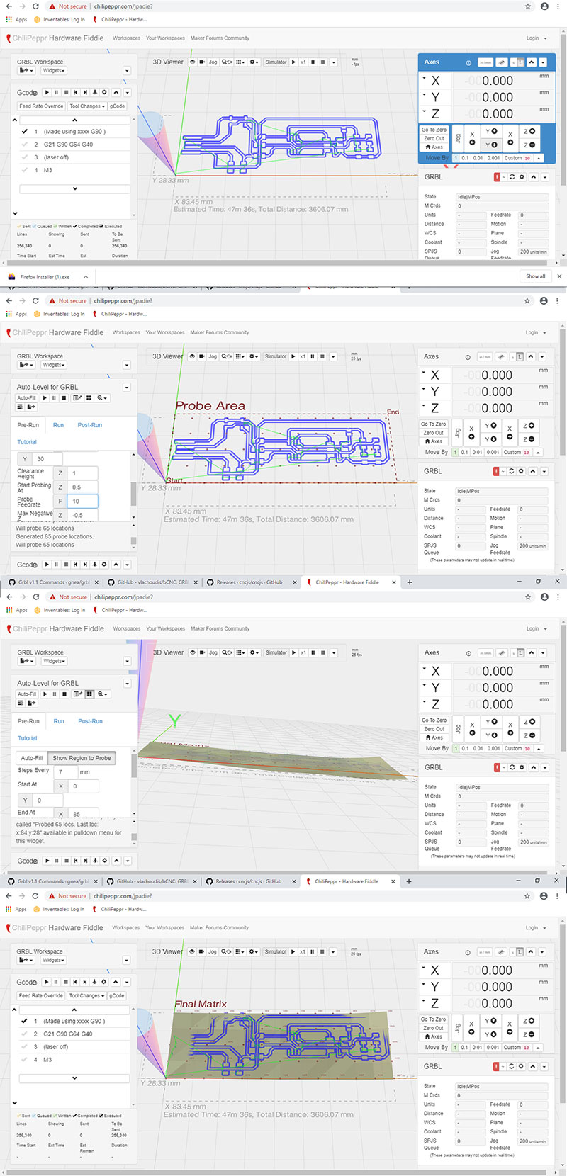
For milling out the profile, we import the profile gcode previously generated in flatcam, change the bit on the mill and proceed with the milling, as no further leveling is needed.
Stuffing the Board
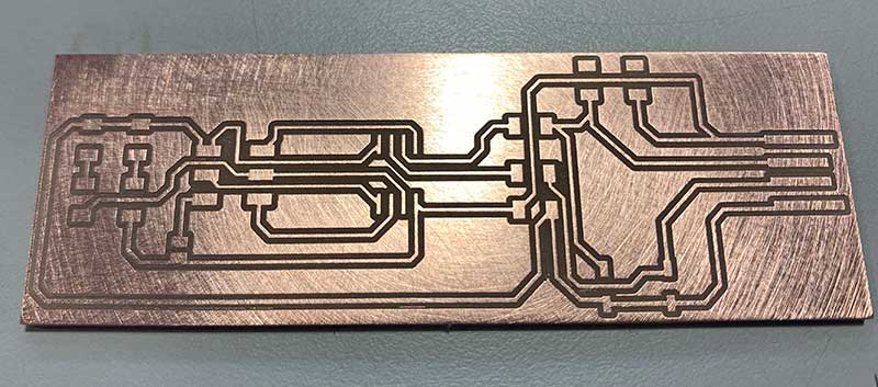
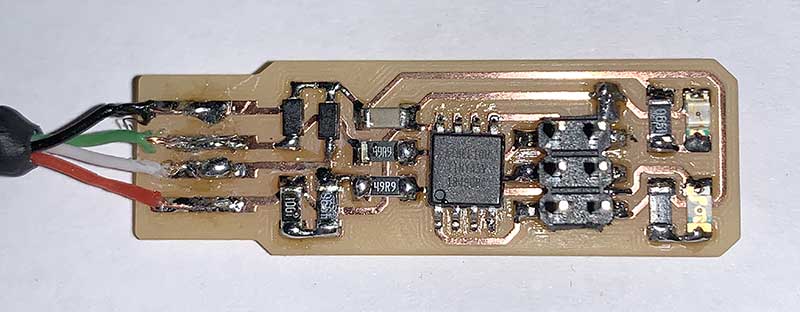
After cleaning out the burr from the mill, and removing some of the thinner copper lines and islands lift behinf, this was my first milled pcb. I didn’t worry too much about the shape of the board as it was recommended that I solder a usb cable to the terminals. In later attempts I did measure and cut the board so it would fit a usb socket or extender cable.
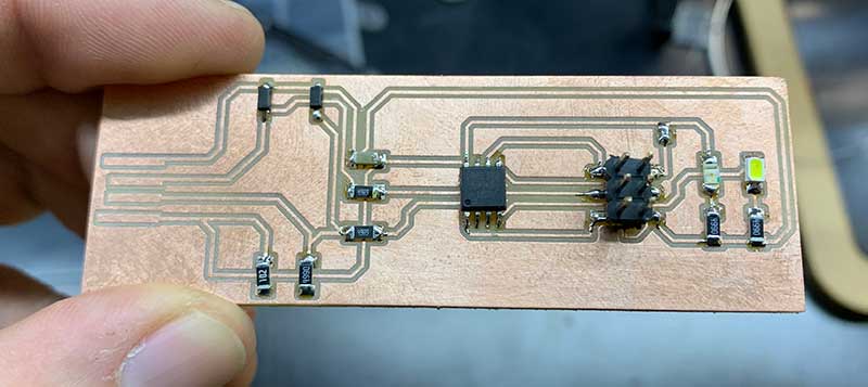
After the components had been soldered to the board
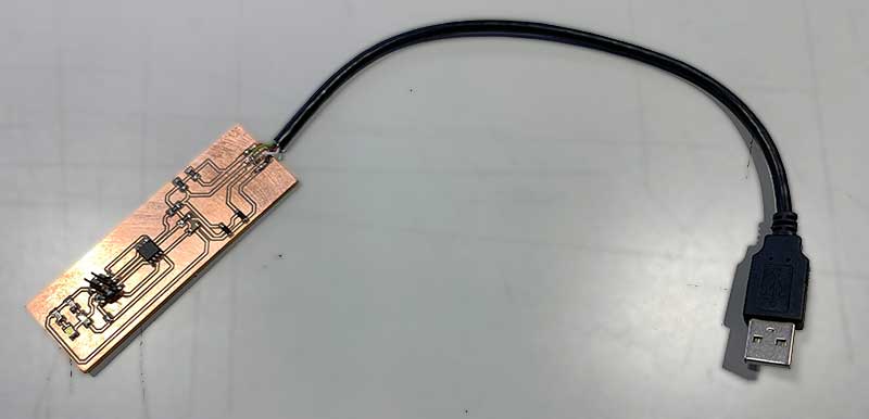
With USB Cable soldered
After visually cheching the solders, traces and components, I followed up by testing each connection using a multimeter on the continuity position. Once satified, I moved on to the next step.
Programming the Programmer
Following Bryans instructions, I downloaded and installed CrossPack as I’m working on a Mac, then downloaded the Firmware. Using the default values in the Makefile, as it matches my programmer, I ran the make all command, which produces the Hex file that would be flashed onto the ATtiny45. after it had compiled, I plugged both the existing ISP Programmer and mine with an ISP Connector and to both USB ports on my computer, and flashed mine using the command make flash in terminal, which ran without errors. Yet, when I had only my newly flashed programmer connected to the computer, it would not show up. Fail. I thought I messed up some solder joint, as it was my first attempt. I tried re-flowing the solders, but it got so messed up that I decided to start again.
So I started redrawing the circuit in Eagle, making it smaller as my first attempt had quite a large distance between components ant took a while to mill. I added a common ground and this time I also made the exterior cut so that it would fit in the USB extender.
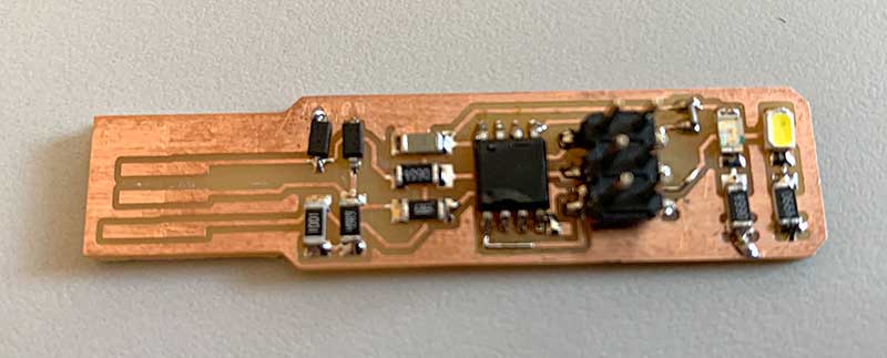
I can’t remember exactly what went wrong with this one, maybe I didn’t manage to flash it, or I did but it wasn’t recognized, or I botched the soldering, something happened, because I redid the whole thing, redrawing the circuit without the common ground. After a lot of trial and error, soldering, re-flowing, testing, and some dark wizzardry from my Fab Manager Filipe Silvestre, we finally got a breakthrough, getting it to be recognized in the computer.
Final Version, working!
This was a hard week.
2022
Repeating Electronics Production
I had trouble with electronics production and completing electronics related projects in 2020, so I decided to start from scratch in 2022. Because of the pandemic, in 2021 I ordered some of the equipment and electronic components to be able to do this independently, but the dificulties persisted.
Now I want to make a modern programmer, explore other design tools and use different software/hardware pipelines, in order to become more flexible in my prototyping abilities.
Deciding which Programmer to make
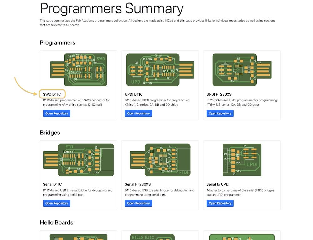
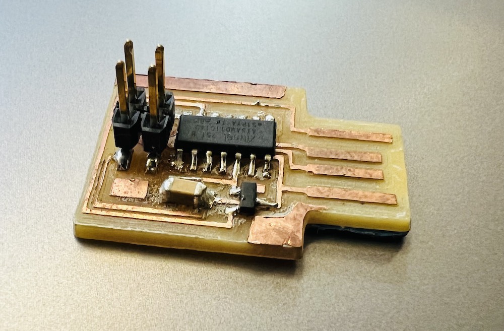
Neil keeps saying the ISP Programmer is old and deprecated, so I decided to make a newer Atmel SAMD11C programmer, as I have 3 of those chips to work with. I checked Programmers Summary to try and decide which one, but there were several different ones.
During Global Open Time, I explained that I didn’t have an initial programmer at hand and asked for suggestions on which programmer to make. Luckily, Quentin Bolsee was on that call and mentioned he was redesigning the SWD SAMD11 programmer, and that if I had access to an Atmel ICE, I could use it to program the programmer. I knew my instructor at FCT Fablab had one, but it meant I had to take a day off of work to go there. Nevertheless, Quentin was just fixing his design so it could be programmed with the Atmel ICE by adding a 10KOhm pull up resistor on the Reset line, and a 100uF from Reset to Ground. I couldn’t quite understand why, but he mentioned the Atmel ICE likes it better that way. Quentin also mentioned that it would be an useful experiment for the Fab Community as a whole if I managed to program his SWD Programmer with the ICE (no presure), so… I took the challenge.
Preparing the Board design files
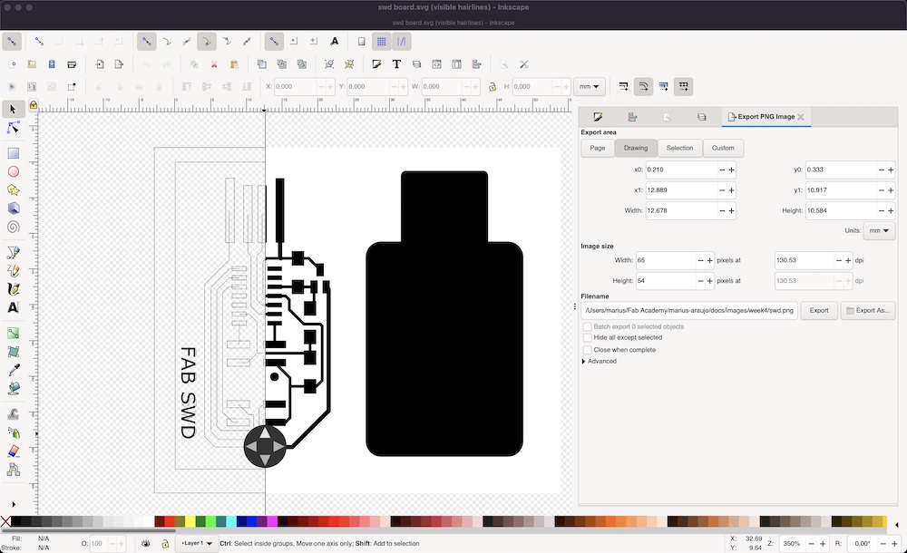
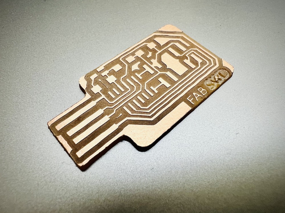
Quentin shared his new design with me, which I then cloned from gitlab. I then checked the schematic in KiCad, opened the board design and exported the front copper and board perimeter as SVG to use in Mods.
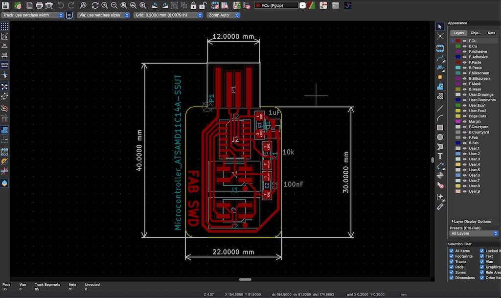
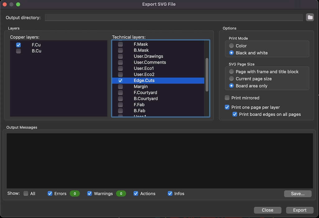
I then edited the SVGs in Inkscape to clean them up, as the Edge Cut layer didn’t come out right from KiCad; it was just a thin line, which Mods didn’t identify propperly. The Front Copper traces worked fine in Mods, but the Edge Cuts needed to be made into a nice black shape.
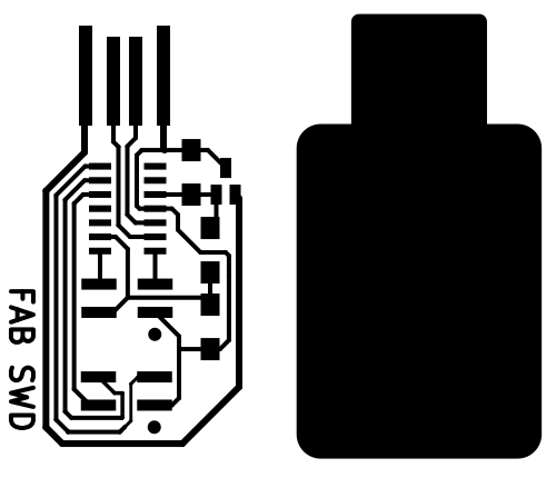
Front Copper SVG
Board outline SVG
Board outlines
I didn’t know it then, but Rico Kanthatham, from Fablab Kamakura, explained during Global Open Time that you can export a nice SVG for the Edge Cuts from KiCad, but you need to create a closed shape in one of the user layers, and not the edge cut layer. The edge cut layer really only allows for a thin line to be produced; the user layers allow for shapes do be drawn, so those shapes can be filled, which is what Mods needs to find the edges and generate milling paths. Nevertheless, if, like me, you like a nice curved shape, it’s much easyer to draw that in Inkscape than in KiCad, at least in my experience.
Machinning the Board
Once I had nice SVGs (or PNGs) of the front copper mill traces and the board edge cut, I decided to use Mods Comunity Edition to prepare the actual milling files to send to the CNC Machine.
The CNC Machine I have is a Genmitsu 3018, which I bought as part of Danielle Ingrassia’s excelent FAb Academy Kit.
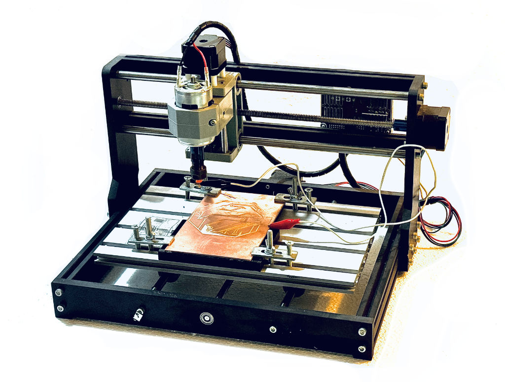
The Genmitsu 3018 has the following specifications:
- Work Area of 300 x 180 x 45 mm (hence the number in the name, 30cm x 18cm)
- 1.3 A Stepper Motors, 12V, 0.25 Nm torque
- 12,000RPM Spindle motor, 3.175mm millbit collet
- Able to sense Z0 on metalic surfaces, with the appropriate Z-probe cable, as well as auto-leveling if the control software is capable
- T-slot 2040 Aluminum Profile working area, with T-Track hold down clamps for work-holding
- 8Bit CNC GRBL Controller
- No inbuilt emergency stop switch, but able to connect one as an upgrade
- No stepper motor jog wheels
- No home or limit switches, but upgradable
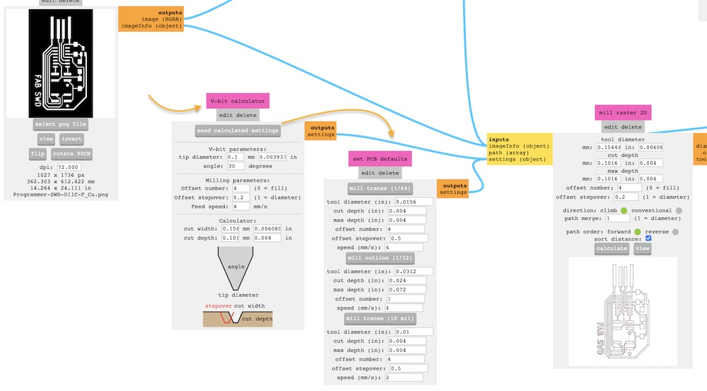
It is a simple GCode machine, so in Mods, I started by opening the GCode > Mill 2D PCB program.
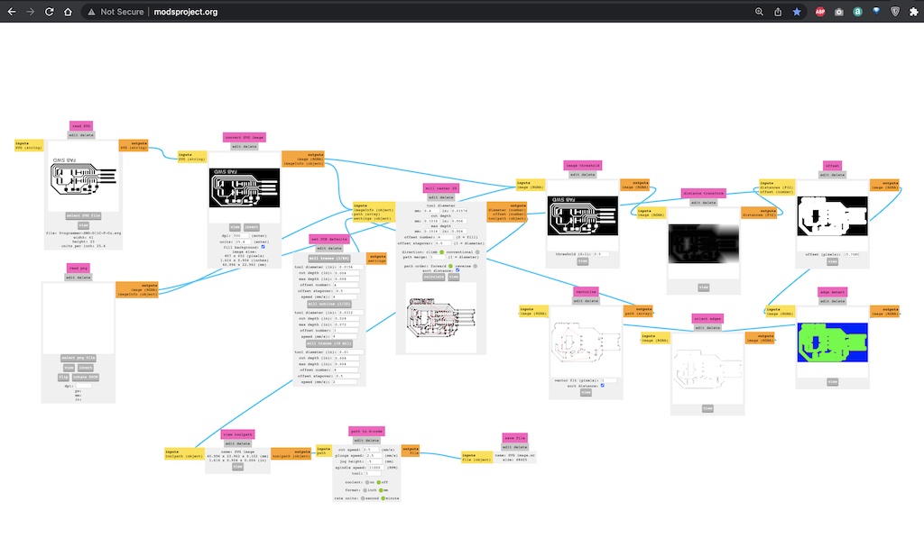
Then I proceeded with these steps:
- Import the front copper traces SVG file
- Changed the DPI to 1000
- Invert the SVG image so that Mods calculates milling paths outside of the traces, not inside
- In the Set PCB Defaults module, press Mill Traces (1/64)
- In the Mill Raster 2D module, change tool Diameter to 0.4 mm, which is what I figured out at the time for my V-Bits, through trial and error (lots of error)
- Leave Cut Depth at 0.1016 mm
- In Path to GCode module, change cut speed:3mm/s
- Jog height : 0.5mm
- Spindle Speed: 12000 (Max of 3018)
- Calculate
- Save resulting .nc file
V-Bit Calculator
I didn’t know it then, but I later dicovered the V-Bit Calculator Module that can be added here and help calculate the width that these bits are going to mill, according to their tip diameter, v-angle and how deep one wants to mill. Given these values, it then sends the width of the mill to the Mill Raster 2D Module, in order to accurately calculate the milling paths. This might have saved me a buch of errors in my trials.
Once I had the gcode files from Mods, I had to send them to the CNC. There are a few options for this, like Universal Gcode Sender, ChilliPeppr, cncjs or even Mods itself.
I had had experience with ChilliPeppr and it’s auto-leveling, which I thought was important, but as it is an online tool, I was having trouble getting it to talk with my Genmitsu 3018 through nodeJS for some reason. I’m sure that given enough time I could have gotten any of these tools to work, but I had to be pragmatic: my internet connection at home isn’t great and I needed as little interference from external issues as possible.
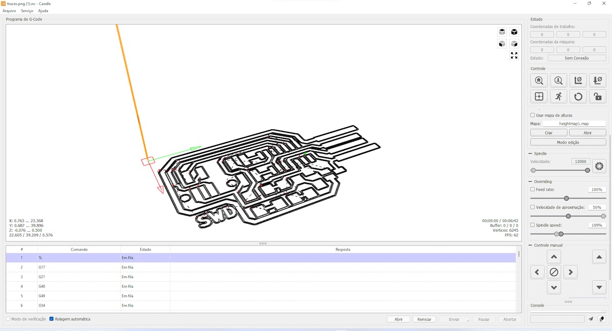
I turned to Candle, an OpenSource program that can be installed on Windows, Linux and even Mac, but most importantly, that also does the autoleveling on the copper board. I thought this was important, as many of my experiments had turned out quite poorly, due to uneven boards. In some areas the mill would go too deep and wide, and in other areas, hardly touch the surface of the copper.
Once I had installed Candle, I proceeded as follows:
- Go to Preferences and select appropriate port (cu.usbserial or tty.usbserial in Mac, or relevant COM port in Windows, baud rate: 115.000)
- Open .nc file saved from Mods
- Set origin XYZ manually (Z-Probe did not store Z0 position in my Mac verion, but did work fine in Windows)
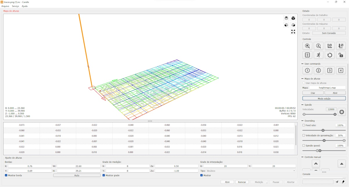
- To Create Height Map: Set border to Auto, probe grid: 10 x 7 or whatever makes sense; Zt (Ztop) 0.4mm (larger distances just take more time going up and back down); leave Zb (Z bottom) at default -1,00.
- Connect Z-probe cable + to the endmill and - to the copper board. Press Probe and wait while Candle does its thing, probing the area that will be milled
- Once finished, press create and Candle will prompt to save the current height map. I think it’s a bug, it should be automatically saved, but you just save a new height map file, then open it again. Exit edit mode and press use height map check mark; it’ll be applied to the gcode.
- Make sure the mill is 1 or 2mm above the copper plate, and press send. Wait while Candle does its thing, milling the board.
- Check results.
When I finally got a nicely milled Front Copper, I repeated the process with a stronger endmill for the edge of the board. I went back to mods, opened the board outline SVG or PNG, inverted it, selected Mill Outline and repeated the steps above to release the board from the FR2 copper plate.
Most importantly, one has to be very careful while changing the mill bit, not to force the mechanics too much, so that we don’t lose X and Y axes origins. We will also have to find a new Z-zero position for the second endmill, so that the edge cuts allign nicely with the milled board traces.
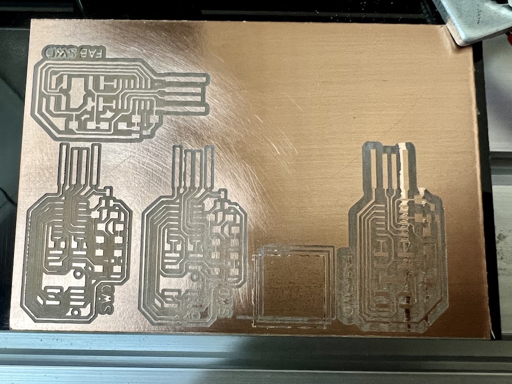
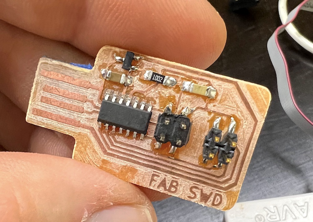
Stuffing the Board
Once I had a milled board, I tried a different technique of stuffing the board. I had bought an SMD Rework Station, which has a hot air blower, and solder paste. I applied some flux and solder paste to the contacts on the board, carefully placed the components on their respective places and let them have it. As soon as temperature was sufficient, the gray paste turned silver and the components slid into place. It was really impressive how much easier it was to solder these tiny parts this way. I did go back with the soldering iron and some more solder to reinforce the joints, but I suspect it might have been enough with just the solder paste. Quite Happy with the results, but still had to program the board.
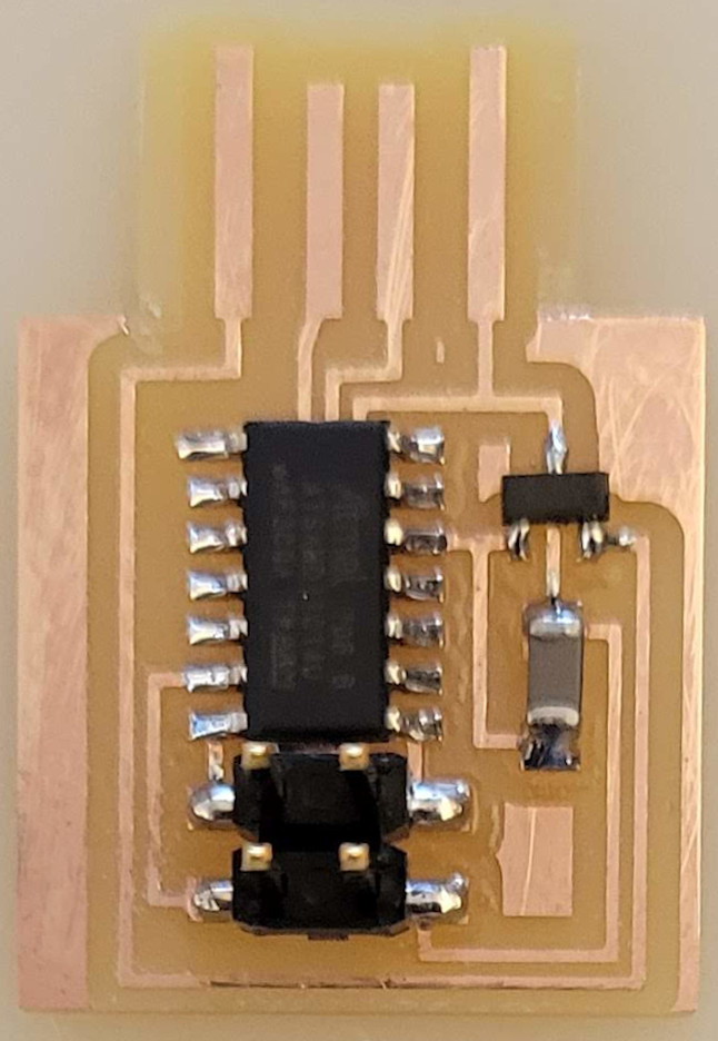
I then milled and stuffed another board, a simple SAMD11C Echo board from Neil’s examples, just so I had something to use my programmer on in case the Atmel ICE actually worked.
Programming the FAB SWD Programmer with ATMEL ICE
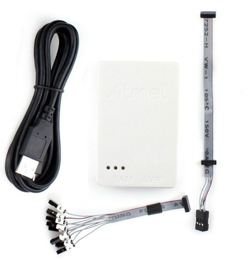
I then arranged to go to the FCT FabLab, a few days later. Once there, the first thing was to figure out how the ATMEL ICE works. It connects to a computer via USB, and it has a cable that splits into 10 little pin header plugs, numbered 0 to 9.
I knew my board has a 4 pin JTAG connector, labeled HOST_DIO, GND, HOST_CLK and HOST_RST. So I had to figure out which of the 10 cables on the ICE orresponded to which of these pins on the SWD. A quick google search led me to this picture.
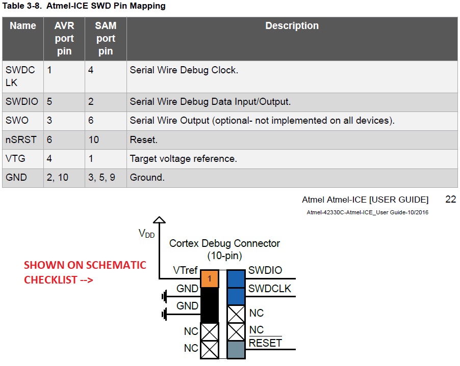
In that picture, nSRST (Reset) is labeled port pin 10, which wasn’t one of the lables. I guessed it had to be the plug labeled 0, so I tried it.
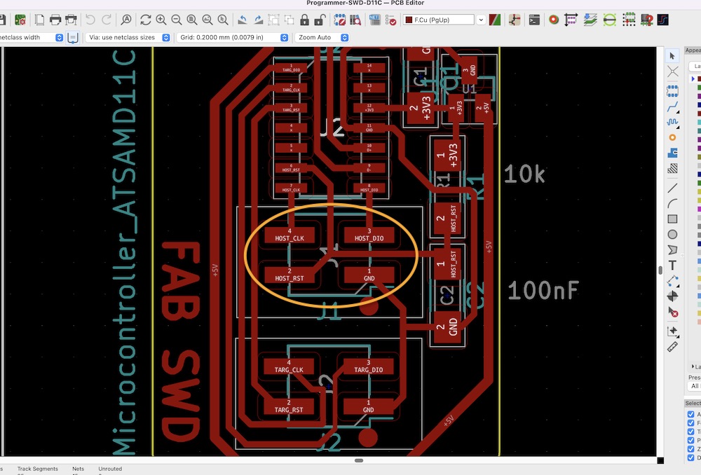
Looking at the Board Schematic, I searched for pin correspondence and connected them with those of the Atmel Ice, in this order:
| Atmel ICE SAM Port Name | Pin | FAB SWD JTAG Name | Pin |
|---|---|---|---|
| SWDCLK | 4 | HOST_CLK | 4 |
| SWDIO | 2 | HOST_DIO | 3 |
| nSRST | 0 | HOST_RST | 2 |
| GND | 5 | GND | 1 |
Alright, the devices are connected, so how do I send a program to the programmer?
While googling the Atmel ICE, I came across Atmel MicroChip Studio, which seemed like a tool to upload firmware to microcontrollers with the ICE. Nearly 1Gb installer download, and it seemed to install a bunch of drivers as well.
I opened the software, but it seemed really complicated to use, so I went back to Quentin’s instructions on how to flash the firmware. He mentions two methods, EDBG and OpenOCD. I decided to try EDBG first, and if that failed, try the other one. I followed his links to download Alex Taradovs Free DAP binary, which is the firmware that will live on my programmer and make it function as such, and also EDBG, of course, which is a surprisingly 527Kb small command line application.
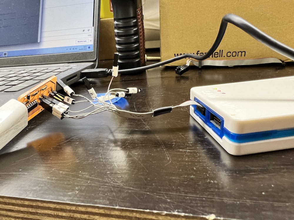
Atmel ICE was connected to my virgin board via the pin header plugs, to my computer via USB, and my board was also connected to a USB extender to the same computer, because it also needs power in order to be programmed.
I opened a terminal, navigated to where I’d downloaded edbg and the .bin file, typed the command like Quentin describes (I did change the command to reflect the edbg’s name as installed, edbg-windows-r32.exe instead of just edbg), and the result was pretty much immediate:
C:\> edbg-windows-r32.exe -ebpv -t samd11 -f free_dap_d11c_mini.bin

Debugger: ATMEL Atmel-ICE CMSIS-DAP J41800058652 1.0 (SJ)
Clock frequency: 16.0 MHz
Target: SAM D11C14A (Rev B)
Erasing... done.
Programming.... done.
Verification.... done.
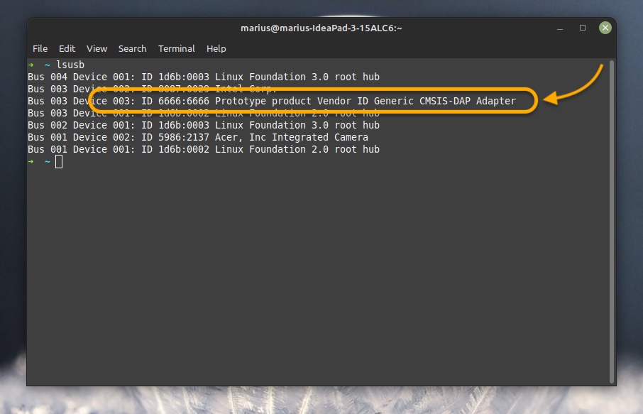
I checked windows’ device manager, but I couldn’t find where the programmer was. Yet, when I plugged and unplugged the USB extender, windows would make that sound like when you plug in an usb device. I checked on a linux machine, opening terminal and typing
lsusb
and sure enough, a generic CMSIS-DAP adapter would show up
I was really stoked. I then proceeded to use it as a programmer. I downloaded the Sam BA Bootloader as Quentin described, and proceeded to connect my simple hello world board to the new programmer, and both to USB. Then, repeat the command EDBG to flash the bootloader file to the new board.
It was flawless. To be continued on Electronics Design week.
Checklist
Group assignment
- Characterize the design rules for your PCB production process: document feeds, speeds, plunge rate, depth of cut (traces and outline) and tooling.
- Document your work (in a group or individually)
Individual assignment
- Make an in-circuit programmer by milling and stuffing the PCB, test it, then optionally try other PCB fabrication process.
Learning outcomes
- Described the process of milling, stuffing, de-bugging and programming
- Demonstrate correct workflows and identify areas for improvement if required
Have you?
- Linked to the group assignment page
- Documented how you made (mill, stuff, solder) the board
- Documented that your board is functional
- Explained any problems and how you fixed them
- Included a ‘hero shot’ of your board