Electronics Design
Assignment List
- Group Assignment ☐
- Use the test equipment in your lab to observe the operation of a microcontroller circuit board ☐
- Individual Assignment ☐
- Redraw the echo hello-world board, add (at least) a button and a LED (with current limmiting resistor) check the design rules, make it, test it. ☐
- Extra Credit: Simulate its operation. Render it. ☐
- To Conclude & Reflect ☐
Group Assignment
We had a short but intensive review of the basic components that we might encounter while designing the PCB board. As follows
Dc vs Ac Power source. Where the common house hold uses AC and the common gadget uses DC. The diverence in voltage change each has, where AC is always a sinusoidal wave around the 0v mark and Dc is more of a square drops and increases (never under 0v)
One great confusion I had : What capacitors actually do. Resulting from the schematic on the 7.1 tutorial I followed. The overview was helpful but my electronic preparation is a tad weak still. As a result I found this Youtube Channel that added to my knowledge: AddOhms
Individual Assignment
The development of this week: Create a Self designed electronic design.
In this case I decided to use the circuit form the "fabacademy Tutorial Section" One that was recently brought to my attention and plan on use continuously form now on. Either way: I followed every step of 7.1 - Introduction to eagle.
The reasoning behind it was: It has several inputs and outputs I'm going to use in the following weeks. It can be used in the Arudino environment (I later learned) becoming super advantageous. Its not too big of a project and will be able to complete in time.
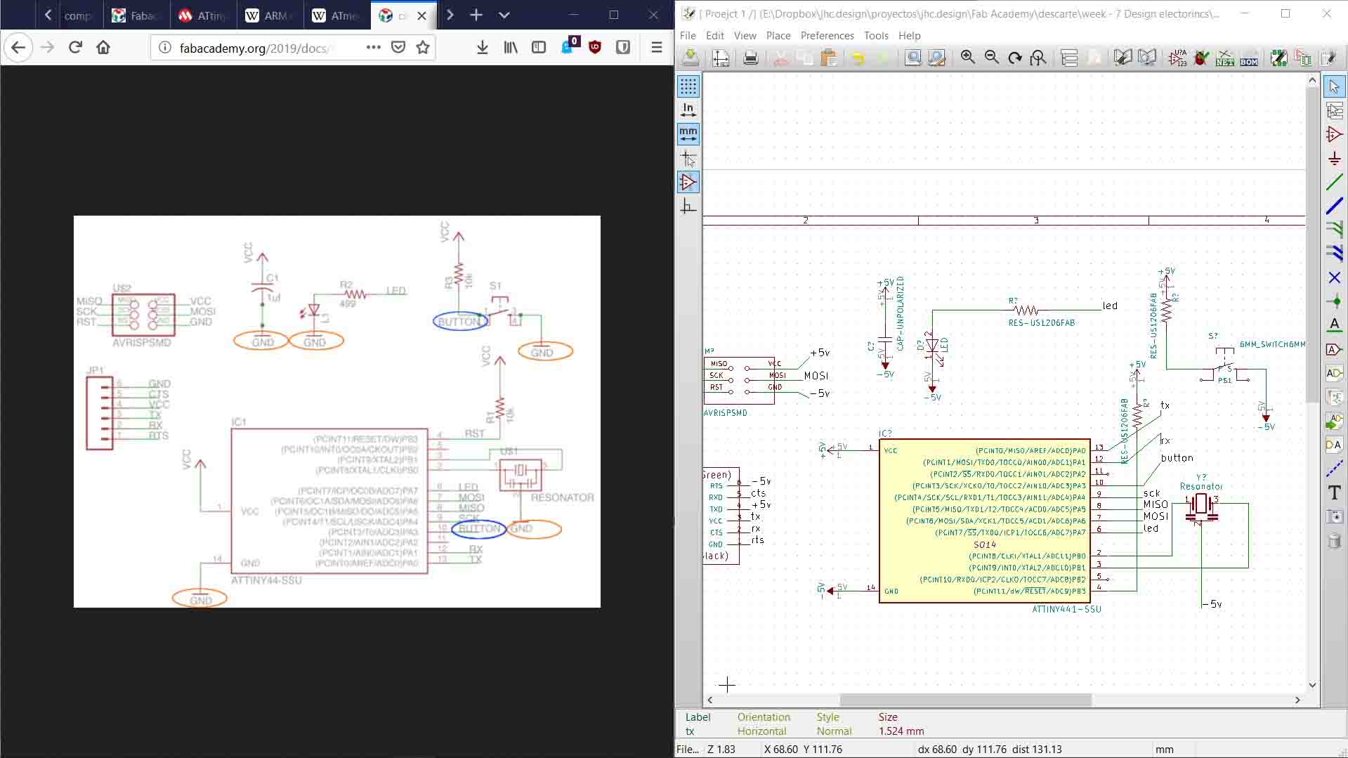
The Components list.
| 1 | 1 uf capacitor |
|---|---|
| 1 | Atmega 328p |
| 1 | 6mm button switch |
| 2 | 10k resistance |
| 1 | 499 k resistance |
| 1 | red LED light |
| 1 | 20k hz resonator |
| 1 | isp 2x3 pins, males |
| 1 | ftdi header 1x6 pins, females |
I started on drawing the schematics in Kicad, an open source software for electronic design. The Schematic portion was very easy and well.
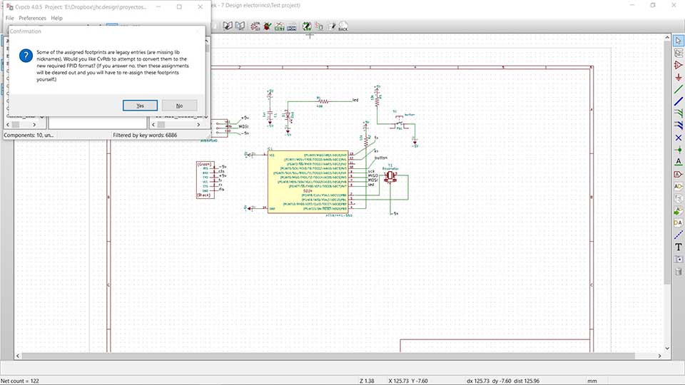
However, at the moment when translating from the schematics to the footprints and the actual path connections I had a big problem that stoped me from doing so. Kicad recognized the connections as not properly engaged. Opening the Electrical Rule Cheaker it seemed so. But after the 3ed re-drawing the same cable and zooming in as far in as possible, somethigng smelled wrong. I was not alone, as my classmates also found themselves in a similar position.
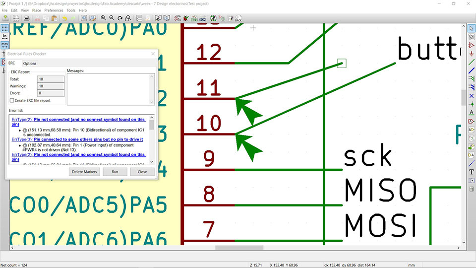
Without the connecting paths correct, the softare will not let you switch to the footprint section of the pcb. After many hours stuck in the same position it became clear a better option was to start again in eagle. Due to the specifics of this problem and lack of mention of it online it seemed pointless to guess the actual problem.
In this case, we as a group used Kicad (the currently open source version of EDA).
We followed the tutorial with slight modifications in the circuits. With this EDA we encountered a hard time translating the finishied schematics and into the actual path PCB design. We found plenty of support about the program, though blog commnets and little about our problem with the official soruce. The source documentation glaced over the issue and i could no follow, or could my classmates. We gave up with using Kicad. It was still early in the week and found greater support for eagle.
In this case we did manage to get the Earlier Eagle version (where it was not yet owned by Autodesk).
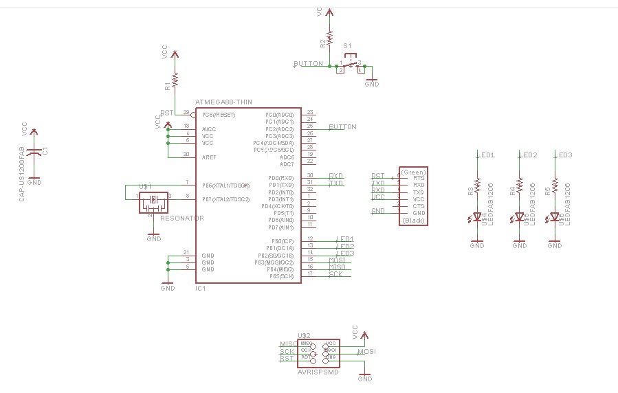
The process between the schematics and the later PCB path drawings was seamless.
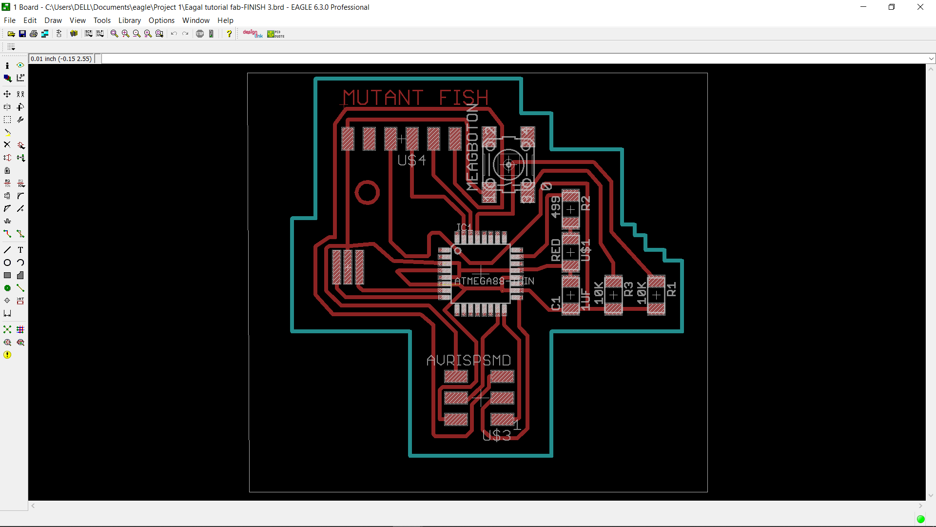
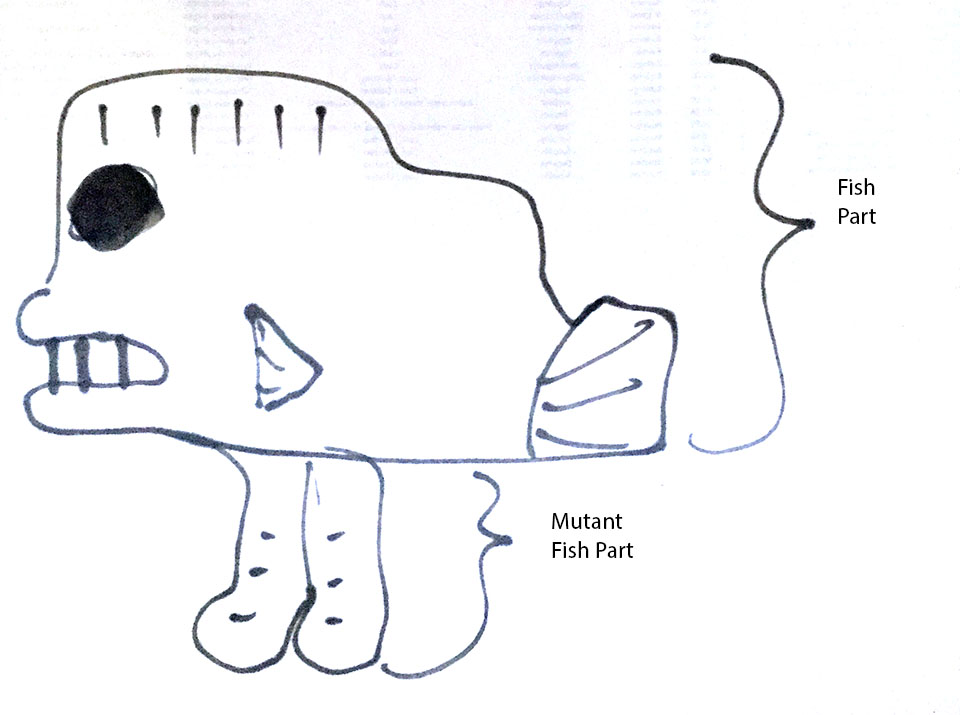
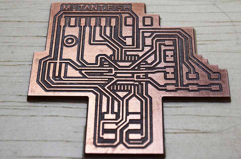
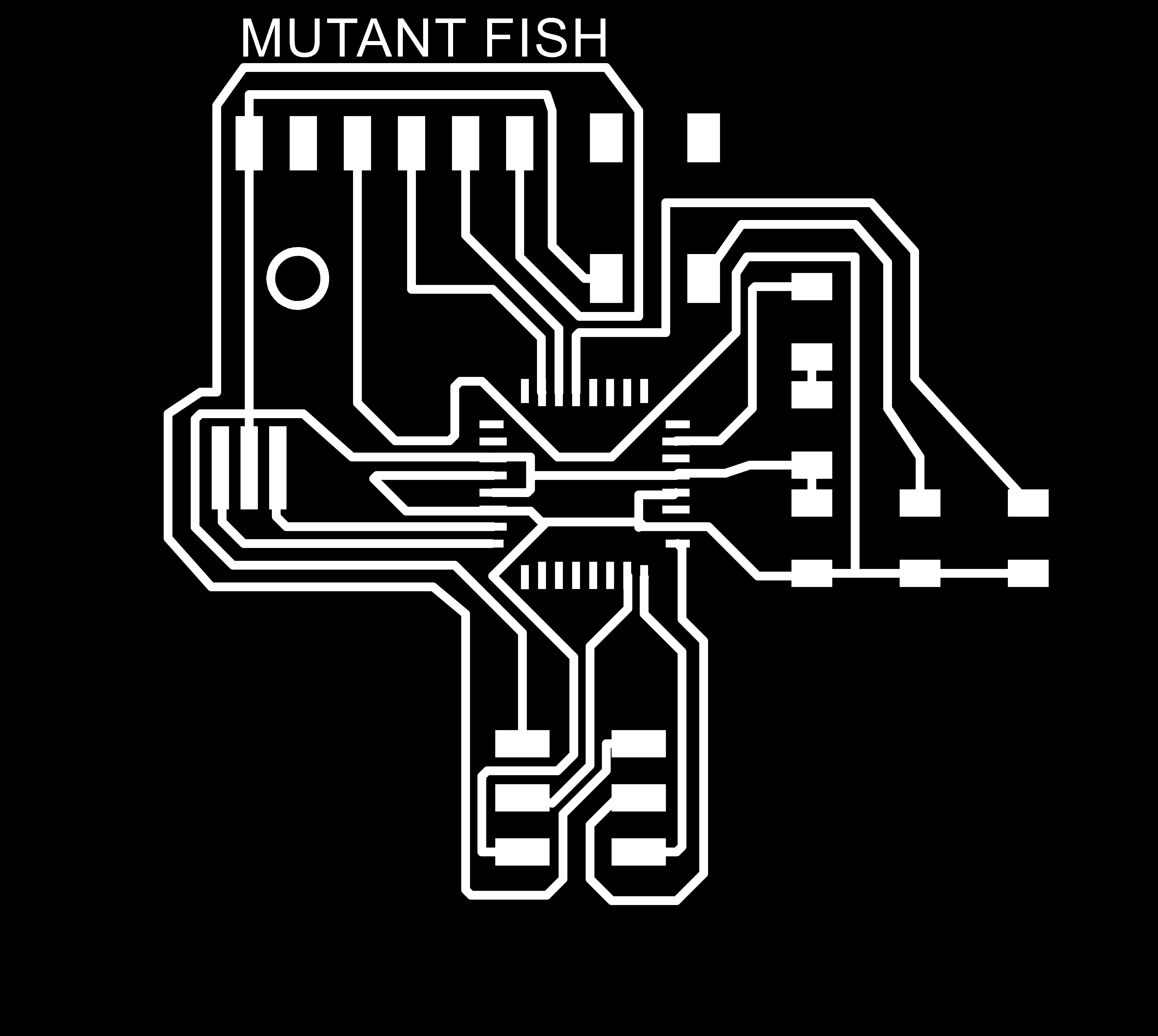
The hardest and most amusing part of the exercise begun. The puzzle of creating a 1 faced PCB with all the components. It was an on going discussion with the group, as everyone had one theory of how to make it easier. The instructors later pitched in with great advice and minutes to midnight the final path for my PCB was created. I did refine it a little to have the paths somewhat more efficient. In the end I saw a mutant fish as such. Either way the "eye" was great pointer to define the Attiny 238 orientation.
.jpg)
.jpg)
.jpg)
.jpg)
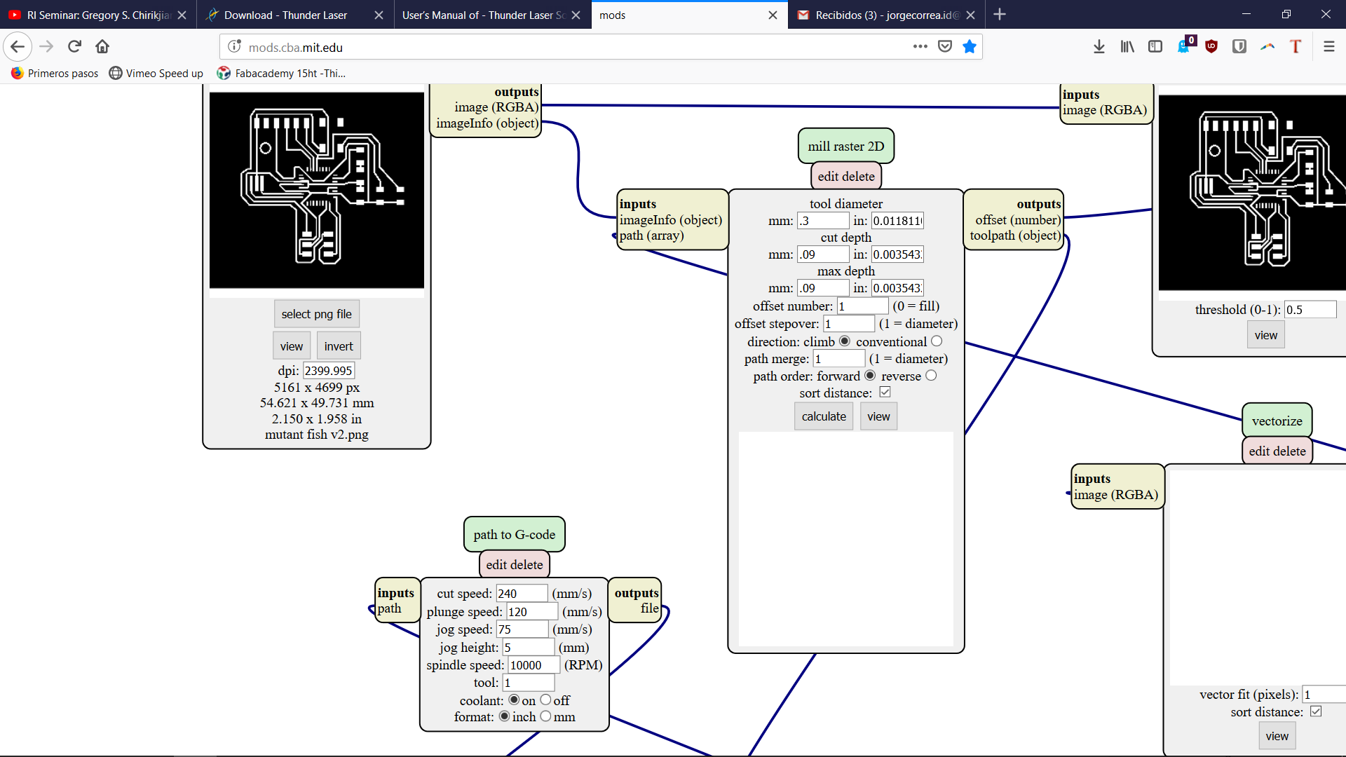
The final design looked like so:
After we load it up into the cnc linux.
Engraved the paths into the pcb creating this monster. The settings where kept form the week 5 electronic production.
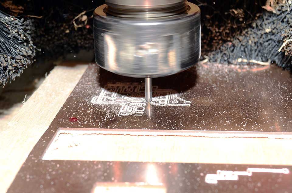
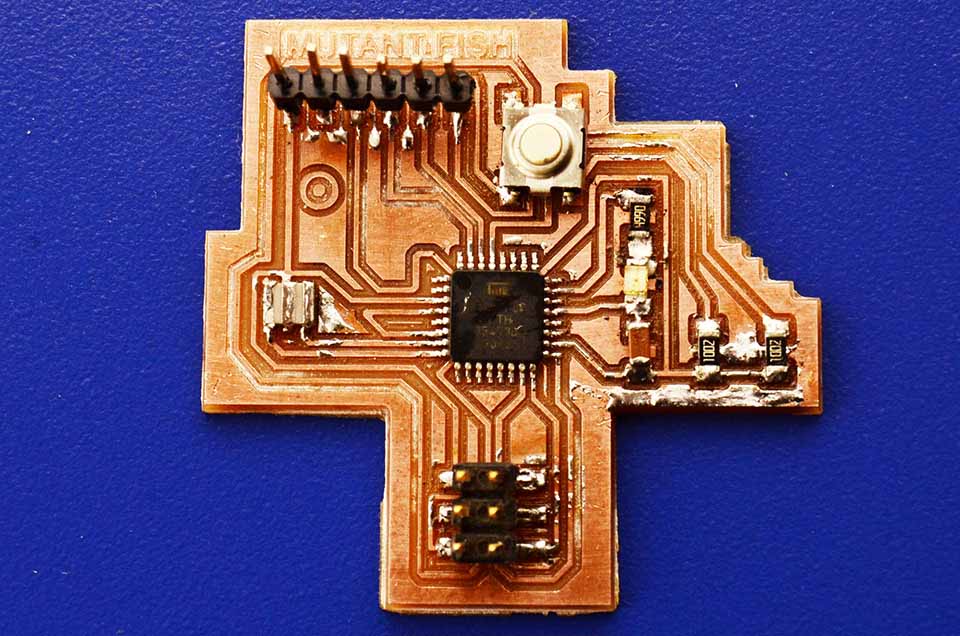
After the final design was edged in the cnc, I sent the same bit to cut. A 60 Deg Pointed V Bit Engraving tool, it was however too thick and actually cut through some of my outer paths. So engraved and cut the PCB board again. And this time made the engraving with a 60 deg pointed v bit tool and the cut with a 30 deg pointed v bit tool, aside in mods I sent a 1mm tool instead of a .35 mm tool bit in order to make the offset of the cutting path add more room without actually modifying the png file. Too bad later on I was not able to tell the distinction and acctually used the broken path pbc soldering on all components and found it easier to fix the broken path with extra sodering material rather than changing the pcb.
To Conclude
This week was a hard yet very interesting week. Much more creative than the electronic production week, and at the same time it all build on that week, highlighting the importance of getting the concepts straight on that week.
Design was supper cool, and the part of placing the paths was oddly satisfying. I think like design, creating multiple iterations was the best way to solve for the problem.
When instead of constantly modifying the paths to fit a specific need, restarting when i got sort of stuck and repeating was the best thing i could have done to solve the path connections quick. With the help of taking a snapshot of the path I could not solve. When i did solve for it, i did the same process and it kept refining until i had something much more condense than the beginning.
I freaking love to sawter picess so small and of my own creating into the board. Headphones on full blast and the window open as the twisers and iron make their thinkg giving electronic life! Yeah I have had probelms, and solved them. As is creating a specific path onto the pcb where there was non, but it was so much fun Im actually glad it happened as my ssawtering abilities and time ot create is only reducing. It is however important to create a case and have a tuperware or soemthing to protect the pbcs otherwise they are so easy to creack the copper off the board is not amussing. Ill be making 3d printed cases from know on for everyithing i create.
I still have to focuse harder in order not to make silly mistakes as cutting the pcb with the wrong bit would be restated. A big loss of time mostly.