Electronic Production
Assignment List
Group Assignment
- Characterize the design rules for your PCB production process ☑
- Make an in-circuit programmer by milling the PCB, program it, then optionally, trying other processes. ☑
- To Conclude & Reflect
Individual assignment
Group Assignment
Defining workflow pcb cnc process
- Drawing / aquire PNG footprints and cutting
- Creating a output for the machine in mods (g-code)
- Earprotection and Eyeglasses and the setupt the pcb board and bits.
- Turning on the machine
- Connection with g code file
- Defining 0x,0y,0z
- Run the auto-level (cnc linux)
- Run engraving code for pcb
- Run cutting code for pbc
- Soldering electronic components
- Test connections in acordance to schemaitcs
- Program final beutiful programer
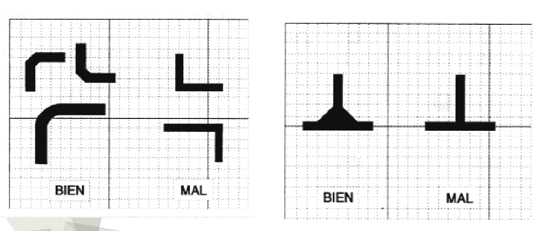
Design Rules for pcb's
So, some practical guidelines that might come in handy earlier on than later are some practical design rules to take into consideration while drawing paths and schematics in the pcb. Find this clever pdf of the DTE University Here. All gread advice given by out instructor Alex.
Soldering tutorial
The initial group was a general review about the concept and key points for soldering. As a group and the instructors, we talked about past experience and great tips on soldering.
- Understand that heating too much will brake the pcb useless
- The importance on maintaining cleanliness in the tip, and the proper amount of soldering material (flux) for different components.
- Understand the point where the flux and the soldering material changes from solid to liquid (by surface brightness) and the concept of the surface tension going on that creates a abrasive bond between metal components and a replant action with the pcb's core fibers.
- We later had a hand on tutorial on the subject in order to properly understand.
.JPG)
.JPG)
Line test - The G code
- The line test is meant to show the accuracy and limits of the tool and tool bits. It's a relevant learning approach to actually creating a PCB boards and a simple way to using a cnc
- We joint as a group with the instructor and analyze the different features the mods programing had to offer
- Reviewing the diverse options and wide range that this snippet of code could do. I was honestly impressed, as I was already a lot of CAD and Technical Drawing work that would have had to be done to replace the .png. It will still be done, yet a picture as an output is brightly simple and exact at the same time.
- Either way we also went through the parameters and the functions to use in t♠he mods tool.
- In the end, every person ended downloading its own png and creating their own g code to try.
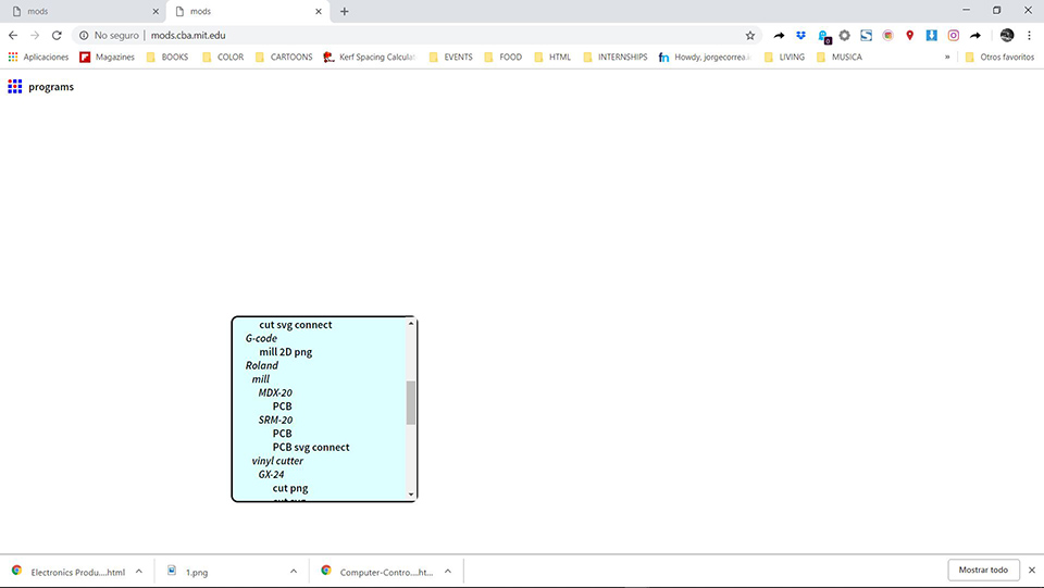
Entering the mods menu
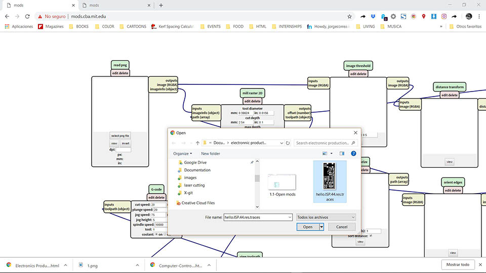
importing the 1st file
General purpose documentations about the engraving parameters
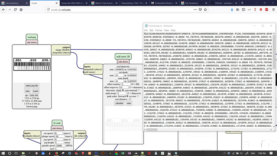
exporting g code
The parameters for Engraving are: (Using a 30 Deg bit)
- tool diameter: .35 mm
- cut depth: .15
- max depth: .15
- offset number: 3-5 (depending on time at hand)
- direction: climb ☑ conventional ☐
- path merge: 1
- path order: forward ☑ reverse ☐
- cut speed: 300
- plunge speed: 150
- jog speed: 75
- jog height: 5
- spindle speed: 1000
- tool: 1
The parameters for Cutting are: (Using a 60 Deg bit)
- tool diameter: .35 mm
- cut depth: .6mm
- max depth: 1.8mm
- offset number: 1
- direction: climb ☑ conventional ☐
- path merge: 1
- path order: forward ☑ reverse ☐
- cut speed: 300
- plunge speed: 150
- jog speed: 75
- jog height: 5
- spindle speed: 1000
- tool: 1
Line test - The Making!
.JPG)
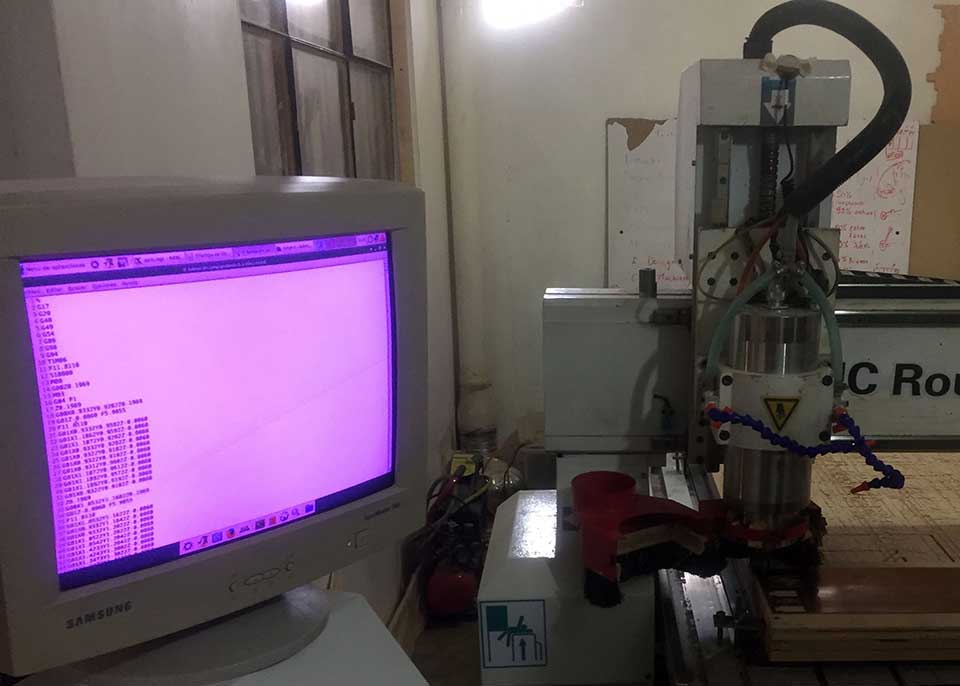
Opening the file in Linux was a slight turn of events from the windows base OS I'm accustomed to.
.JPG)
Loading the software in the CAM, setting the x,y & Z coordinates to Zero in order to start the machining process.
.JPG)
.JPG)
Placing the spindle into it's tightening screw before placing the bit becomes not only a commodity but a safety measure for the bit and the operator's hand.
On the left we see the 30 deg bit, we used to engrave. On the right we see the 60 deg bit. In this case we used the longer bit in order to cut because the 30 deg bit cuts much thicker line and using it only on copper preserves the edge.
In order to set up the Z-axis, to zero we added a bit of code inside the g-code. This part of code created an electrical close loop when the bit touched the pbc board. Below we see the brass sensonr on top of the pcb board.
.JPG)
.JPG)
We did hoverer had to play around plenty in order to get the right milling parameters. Bottom left was too light, bottom right was to deep and top left was the final PCB we cut off and shown under. Mostly we tinkered with the bit's depth from .1-.15. Later modified the bit's tool diameter: from .1 to .3 and finally to .35. We see the burr as a result of too deep of a cut.
Time to set up the tooling for the milling to occur. In this case a v Milling bit at 60 deg of inclinations. The grat advantage of this bit was the option of cutting and engraving. It was later revelied flat head milling bits are hard to find in Quito. Most lightly as a relult of lack of technological manufacturing and high import taxes in place.
In this case, to fully define the Zero Axis we used contact with the bit. As part of the programming CAM (added by linux cnc) the machine recognized the zero after the initial instructions.
.JPG)
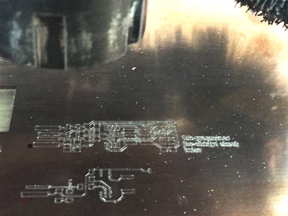
Here we see the final product: The Line Test. Unfortunately we did the engraving tests all at once, and then the cutting resulting the cut to be slightly un-aligned with the PCV's engagements. It is still readable. We are able to see how the resolution we managed to get was 2 lines before the .001cm line (white space). And the thinest coper path was closer to .010 cm. Still very impressive. I doubt that any component we will be using requires such precises and thin connection.
In this case the limit of the resolution is dictated acording to the soldering technique of the craft peroson (me) and the components.
Engraving Production
The final cutting parameter where experimented by the group but could not have been proper wihtouht the help of Alex, and his final parameters for each bit. Super Important
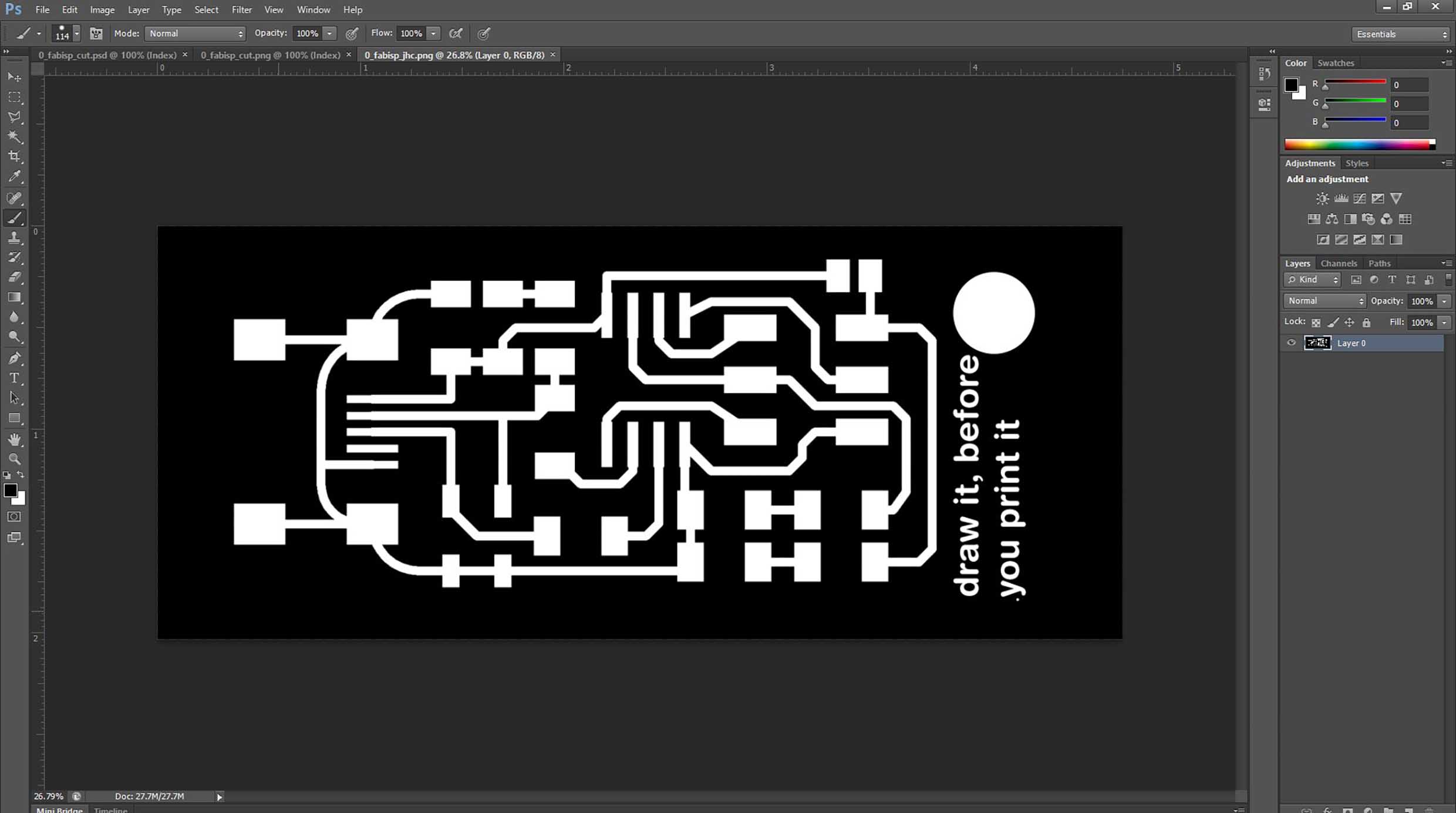
After the group assignment, it was individual turn to create our personalized pcb. In my Case, I dedided to initially modify Alex's ISP programer.It all went south when After prepering the png eddition you see on the side, the cutting time came and we realized the pcb format was x2 bigger. A simple error in pre-process that hold me back.
As a result of this falure, i decided to go and use Brians Ips - programmer instead as it required 1 less component to salder. And I was getting shorter on time.
Initially the paths became to thin with the png image inverted. Later with the cutting tool too close to the png, so we switched the paramenter from .1 to .3mm.
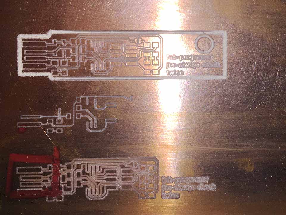
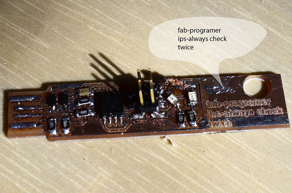
When I finally got to the production of 1:1 scale pcb, I had some later errors as the pahts of the engraving became too small. Due to the unproper post processing in the Mods. Re-processing the image, and inverting the colors at the mod's 1s module the g code was finally ready to cut. What you see on the left is boxed in red the thin paths. Finally we see the ISP proceesor bord. Engraved on it: "Always cheak twice".. Aparently twice is not enough. Let that be the lesson.
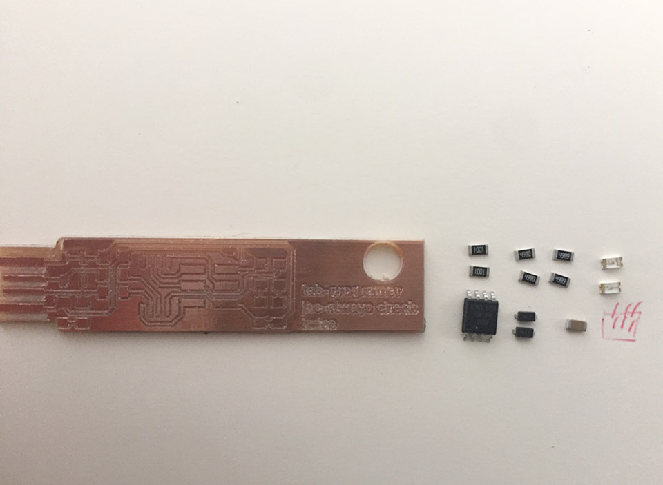
Here are all the components to solder in the board.
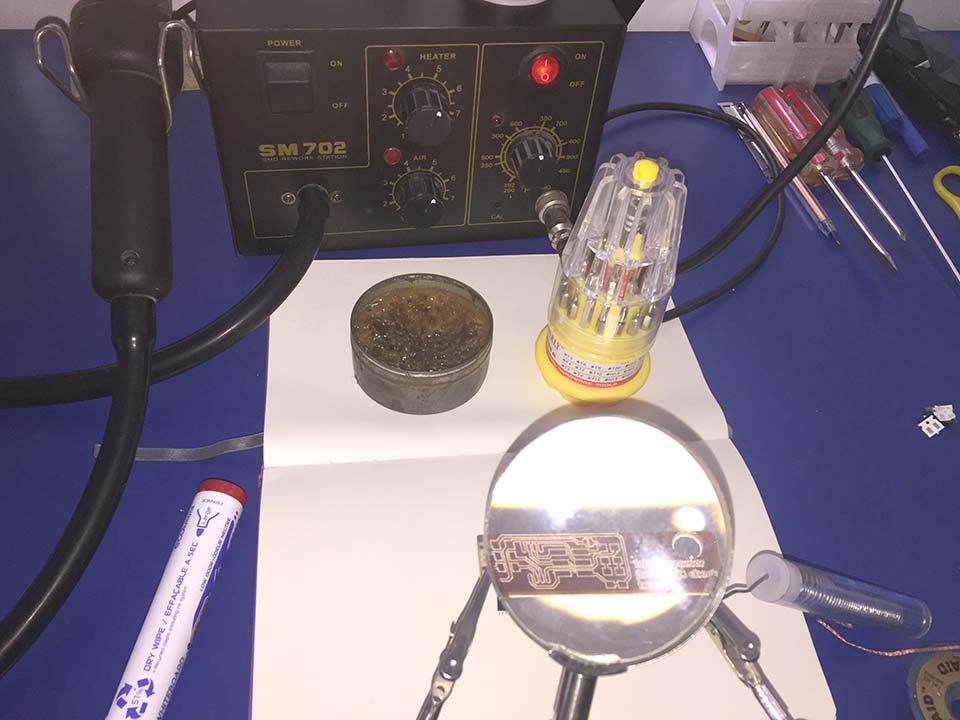
The soldering station setup. It was a couple of hours of figuring out the soldering.
- 1 ATtiny 45
- 2 x 1 kΩ resistors
- 2 x 499Ω resistors
- 2 x 49Ω resistors
- 2 x 3.3v Zener diodes
- 2 x LED
- 1 x 100nF capacitor
- 1 x pins of 2x3 pins
Here is the final result of saldering. If you see in the brige, it was soldered and unsoldered al least 3 times.
Here is the 1st attempt to programming my ips. It failed.
In this case it falied because i did the command res too soon and the ISP's atminy 45 microcontroller was fully blocked.
Later I got a new one and placed it on, only to discover the paths had lifted due to unproper placement inside the bagpack.
The solution in this case was to create another pcb due to its hard damage. You will later see the final result with its corresponding files.
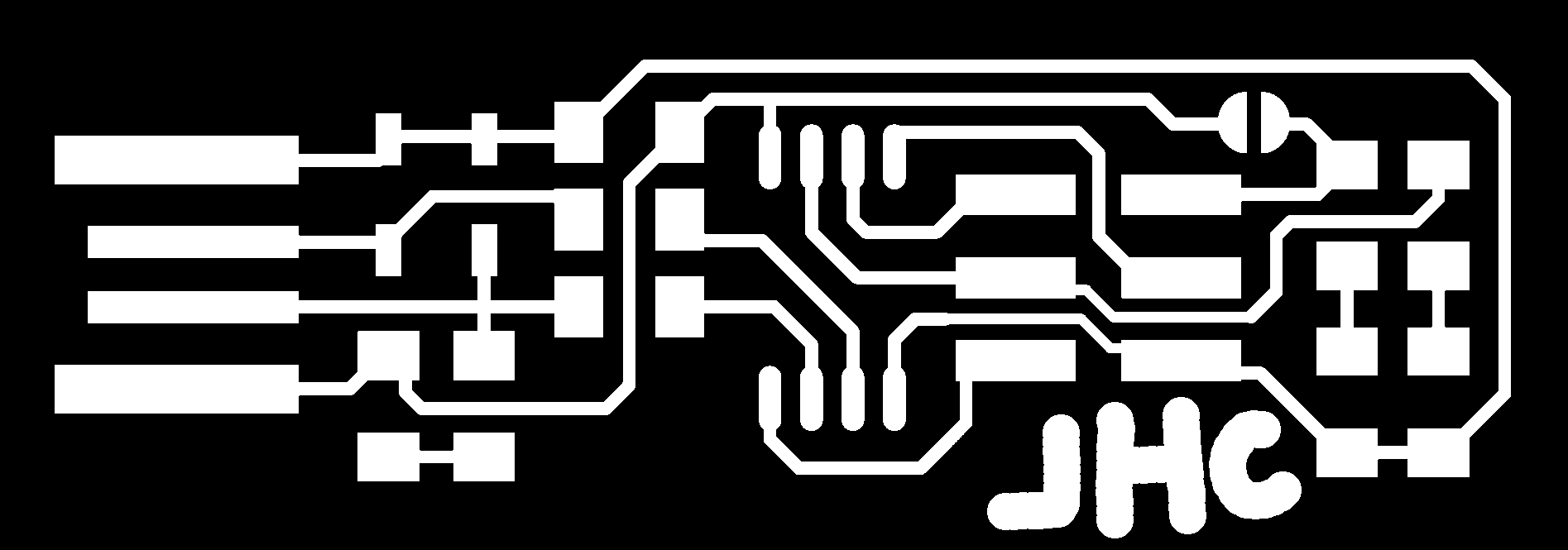
Here is the newly adpated png to send to mods:

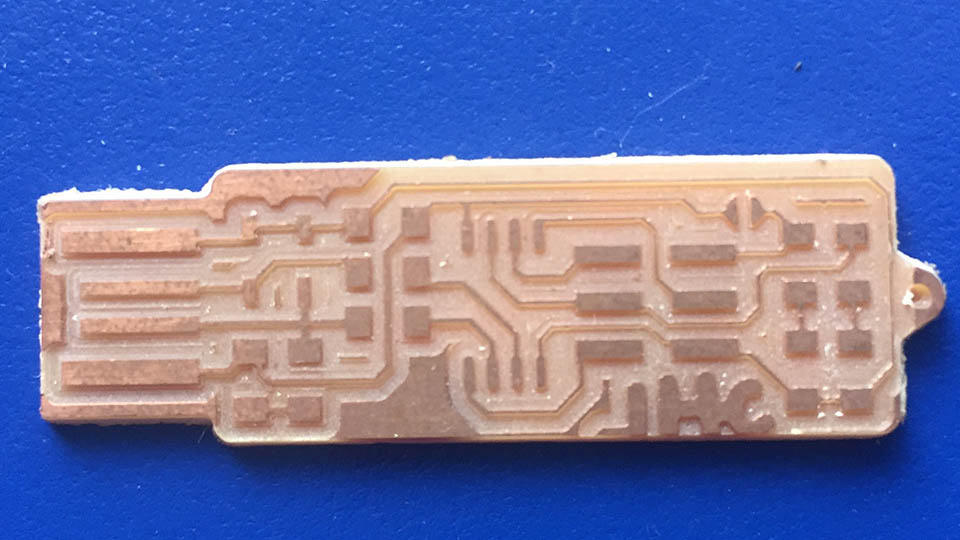
I later unmounted all the componenets from the previous pcb and mounted them on to this final version. (with the exception of the Attiny 45)
.JPG)
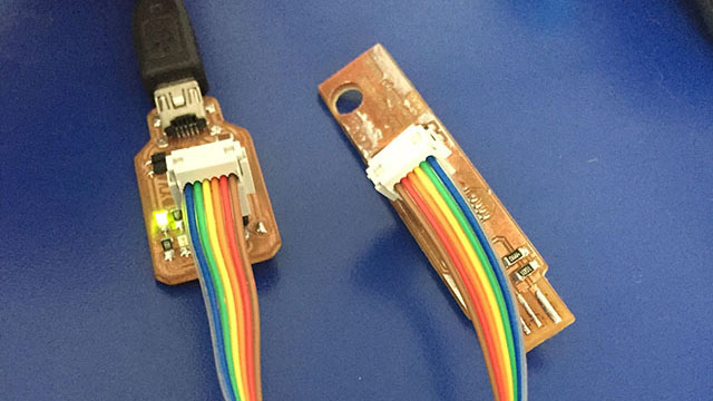
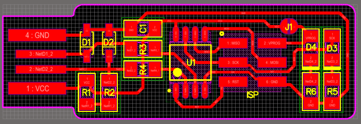
Here is a picture of where everything goes, taken from Brian's page the author of this design.
I later added an aditional 3d Printed protection in order to protect the IPS.
.JPG)
Hero Shot!
Programming
My pc was faulti for some reason and would not let me program in it. I ended programing the pcb in my classmate Danny.
For this programming portion, it became indispensible to follow a tutorial of somebody that had done it beofre. In this case Alex (for all the software portion of the exersice) intially and later Brian (for all the hardware electronics)
0. Install the following programs or paste the files inside the paths require:
- Git (if you dont already have it)
- Atmel GNU Toolchain (AVR 8-bit GNU Toolchain 3.4.3)
- GNU Make
- Avrdude
- Zadig
- Usbtiny driver
& add inside:
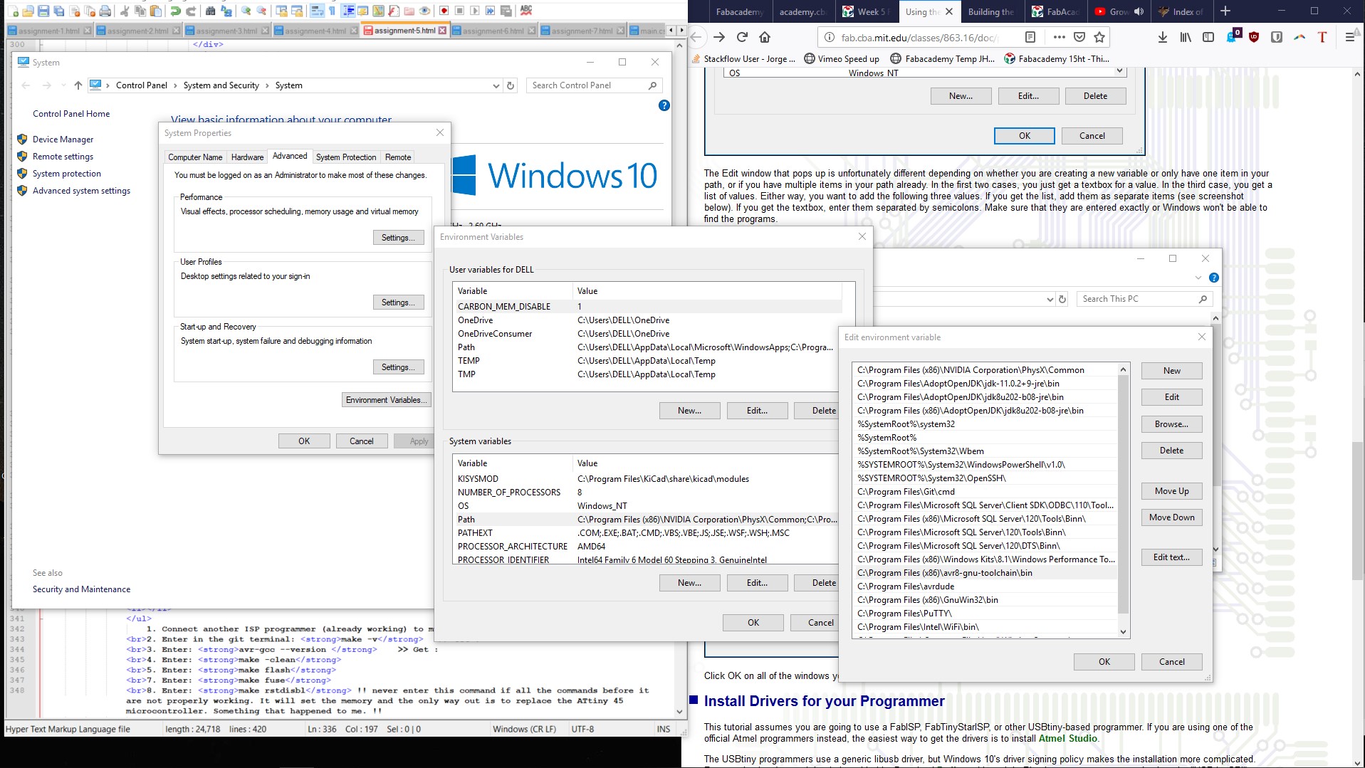
PC folder(right click)
>> System (Advance system settings)
>> Under Advanced tab (Settings)
>> Environment Variables (User variables for dell)
>> System Variables (path: Edit)
New
Inserted the following paths:
- C:\Program Files (x86)\avr8-gnu-toolchain\bin
- C:\Program Files\avrdude
- C:\Program Files (x86)\GnuWin32\bin
2. Enter in the git terminal: make -v >> Get :
3. Enter: avr-gcc --version >> Get :
4. Enter: make -clean
5. Enter: make flash
7. Enter: make fuse
8. Enter: make rstdisbl
!! never enter this command if all the commands before it are not properly working. It will set the memory and the only way out is to replace the ATtiny 45 microcontroller. Something that happened to me. !!
Debbuging
.jpg)
.jpg)
.jpg)
Installed the paths in the wrong directory thinking they all looked the same, the are not the same. Install it in the correct place and with the correct path.
.jpg)
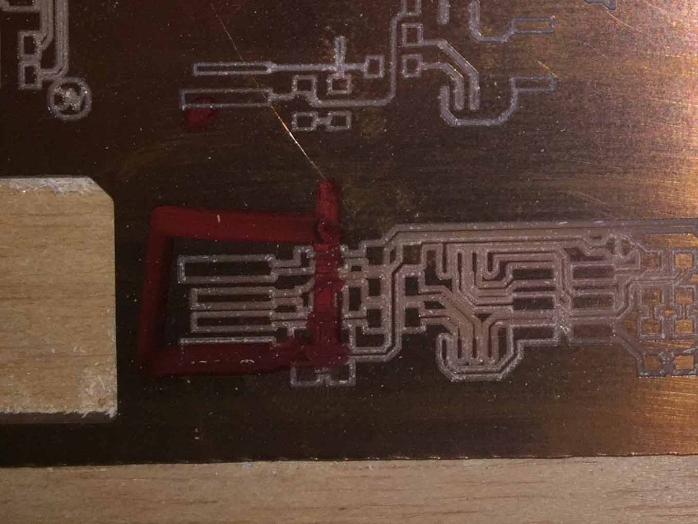
Make sure all the connections in the electronic's side are correct with the schematics. In this case a path on the far end of the usb had broken as a result of using the unproper pcb cutting tool and as a result I had to solder it with excessive materal and lots of pacience.
To Conclude
Cheaking Twice is not nearly enough. How about like 5 instead?
It was a wild week's assignment I actually extended it for about 2 -3 weeks more due to unexpected events that happened along the way. From the initial png image all the way into the assembly and later programming portion. I ended building 2 pcb's and tons of wasted time to get a fully functional pcb. When I saw the final: Reading | ########... | 100 % I knew I was in the right path, but for the final thing to get it to run the make rstdisbl at the proper time to make the ISP work was a lot of reading, guidance and especialy saldering involved.
So much so that it will be a good idea to have a better understanding what the class might be about before the class starts, to be sharp and actually get assignments on time and not weeks later.