5. Electronics production
This weeks assignment is to characterize the design rules for your in-house PCB production process: document feeds, speeds, plunge rate, depth of cut (traces and outline) and tooling. Then we document our work (in a group or individually). We document our work to the group work page and reflect on your individual page what you learned
Group Assignment
The requirements for the group assignment were:
-
Characterize the design rules for your in-house PCB production process: document feeds, speeds, plunge rate, depth of cut (traces and outline) and tooling.
-
Document your work (in a group or individually)
-
Document your work to the group work page and reflect on your individual page what you learned
The group work page including the documentation is here.
Individual assignment
The individual assignment was to make an in-circuit programmer that includes a microcontroller by milling and stuffing the PCB, test it to verify that it works.
The requirements for the individual assignment were to: * Make an in-circuit programmer that includes a microcontroller by milling and stuffing the PCB, test it to verify that it works.
Converting format
The circuit board .svg files were provided by the instructor. The files can be found here.
Creating the traces milling file for the circuit board
In order to cut the circuit board, we need files for the milling machine. The conversion from svg files to a form which has the required information for milling for the machine we are using is done in mods.
I opened mods in the address http://mods.cba.mit.edu in my browser. It is important to select the right browser. I used Microsoft Edge and it appeared to work. Using incompatible browser, for example Firefox, may cause problems. The problems may include images displayed incorrectly or mods not working at all.
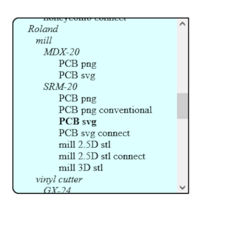
The correct program was open by clicking right mouse button and then selecting in sequence programs -> open server program and then selecting PCB svg under Machines and SRM-20.
The server program opens as a collection of connected modules.
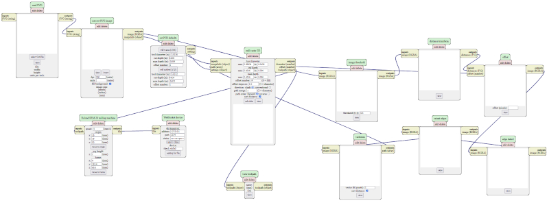
The modules have parameters and the parameters can be adjusted. New modules and connections between modules can be added.
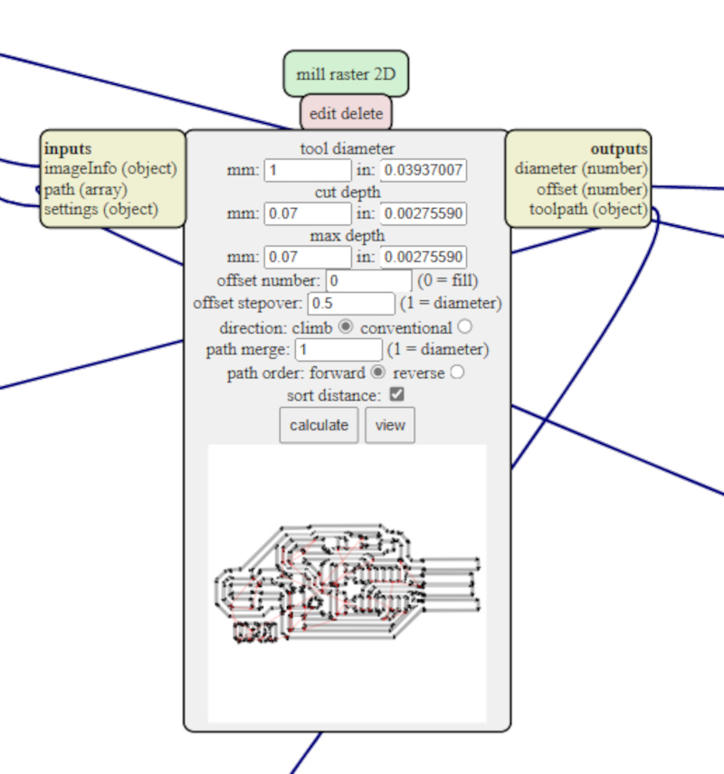
We made some adjustments. We pressed select svg file in the first module (shown in the upper left corner in the previous picture).
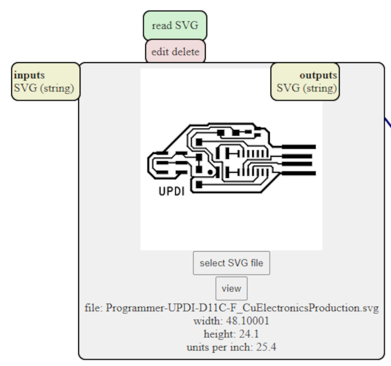
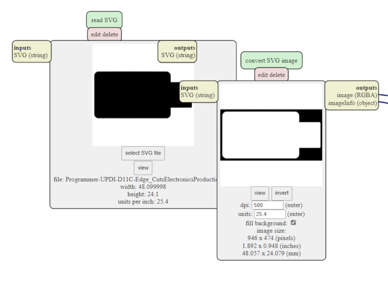
We added Programmer-UPDI-D11C-F_CuElectronicsProduction.svg file. The file contained the trace information of the programmer. Image of the traces is displayed in the module.
Then we pressed view button and added invert to the second module. Inversion was required, because black color in the picture is removed. We want to leave the copper on traces and remove it elsewhere. The convert SVG image module with the inverted traces image is shown in the image below.
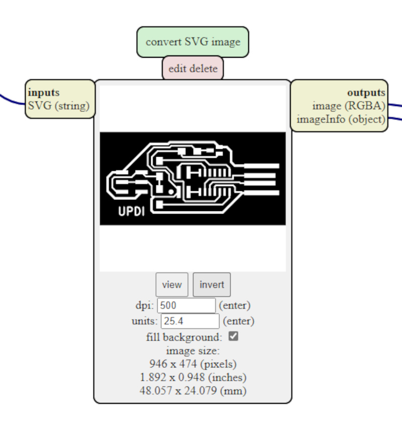
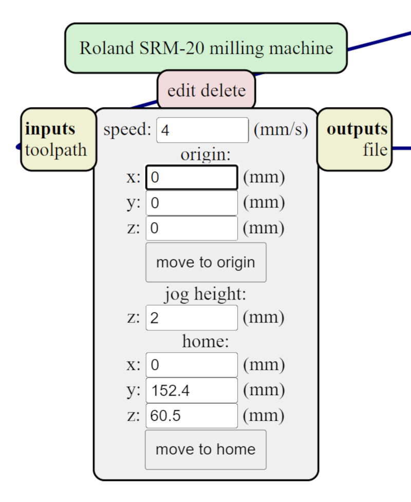
Then we added origin to (0,0,0) in Roland SRM-20 Milling machine module, because it was set to (10,10,10) as default. The bit would not have touched the circuit board with default values.
At this point, the overall view to the image looked like this:
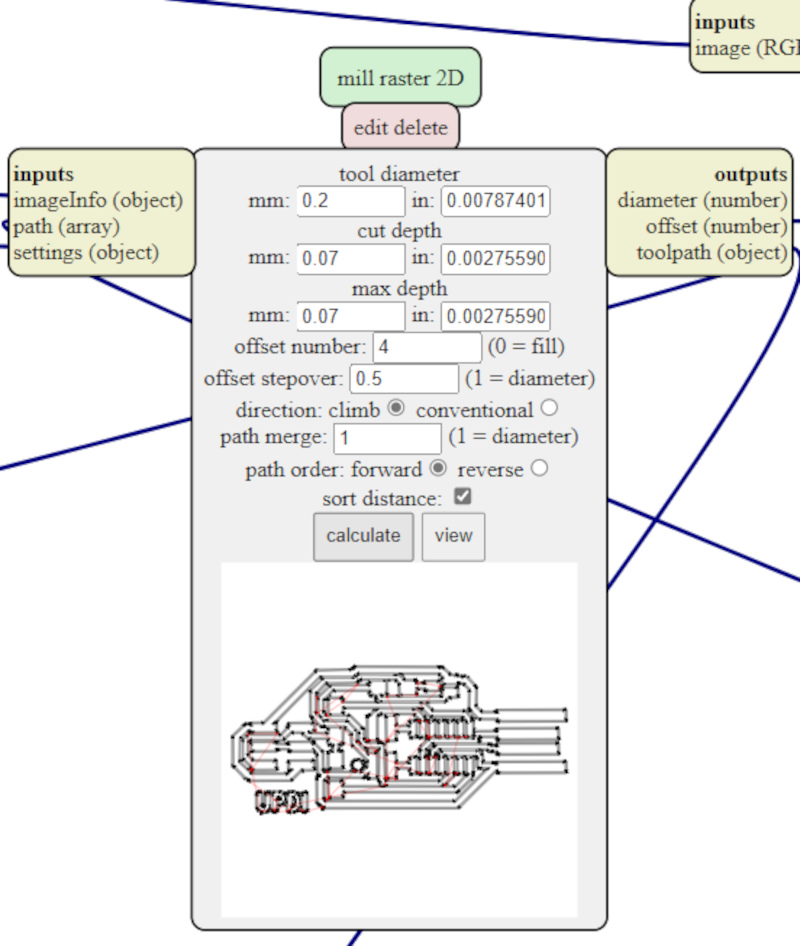
I experimented with different tool diameter and max depth options. Too wide bit could not cut the traces. It appears that in this phase I finally set the tool diameter to 0.2 mm and set the cut depth and max_depth to 0.07 mm.
Then we added a module for exporting the file in the correct format(modules -> open server module* -> file -> save and saved the milling file to usb.
Web socket module was removed and save file module was connected to its place after Roland SRM-20 milling machine module.
Then calculate was pressed in mill raster 2D module. .rml file was automatically saved and the toolpath was shown in the display.
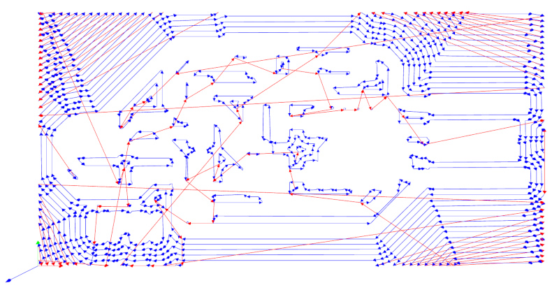
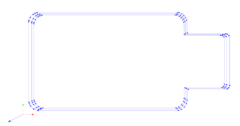
The toolpath is shown below. Blue lines denote the toolpath, red lines show where the drill is moved off the board in order to move the bit over the saved traces. Coordinate axis show the location of the origo and the directions of the coordinates. :
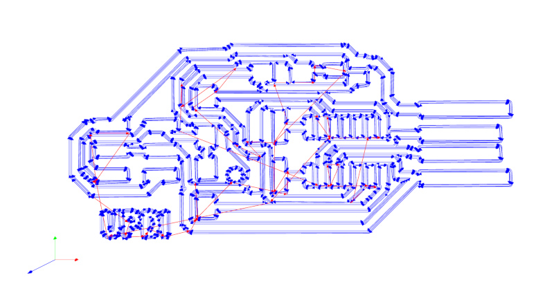
We checked visually, if the traces really were there. It looked ok. The details were there. The saved file was renamed and stored for milling the traces.
Creating the mill file for removing the extra copper
Removing the extra copper around the circuit board was necessary for avoiding the short circuit in case that cutting the outlines would leave some copper on the connector.
The tool path calculations for the removal of areas with 1 mm end mill were performed by the same mods setup but with different parameters. We used offset number of 0 and 1 mm tool diameter in the calculations. Offset number 0 is interpreted as fill.
The toolpath was then calculated and observed. The created .rml file was saved for milling. The toolpath is shown below.
Creating the outlines mill file
The second .svg file was for edge cuts and the outlines. It had to be converted to .rml format as well.
The edge cuts svg file (Programmer-UPDI-D11C-Edge_CutsElectronicsProduction.svg) was selected in the read SVG module. The image was inverted in the convert SVG image module.
Mill outline was selected in set PCB defaults file.
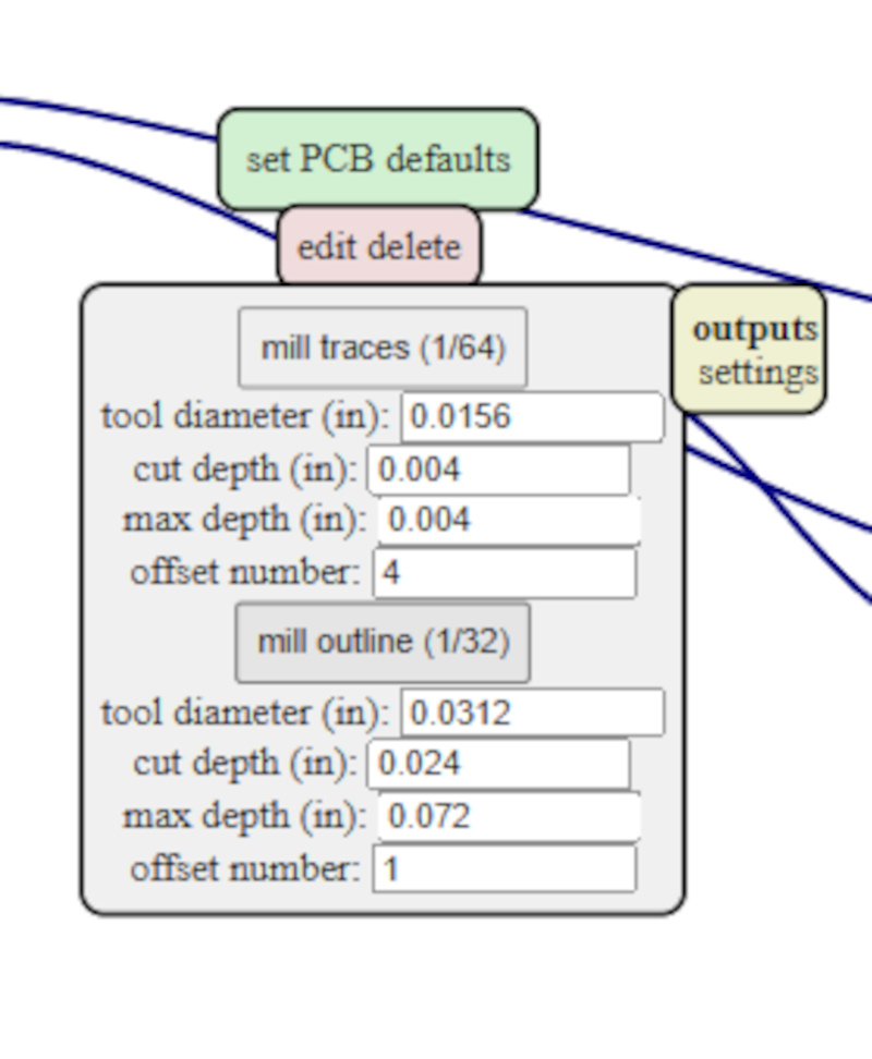
In the mill raster 2D module, cut depth was set to 0.6 mm and maximum depth was set to 1.7 mm. Tool size was set to 1 mm.
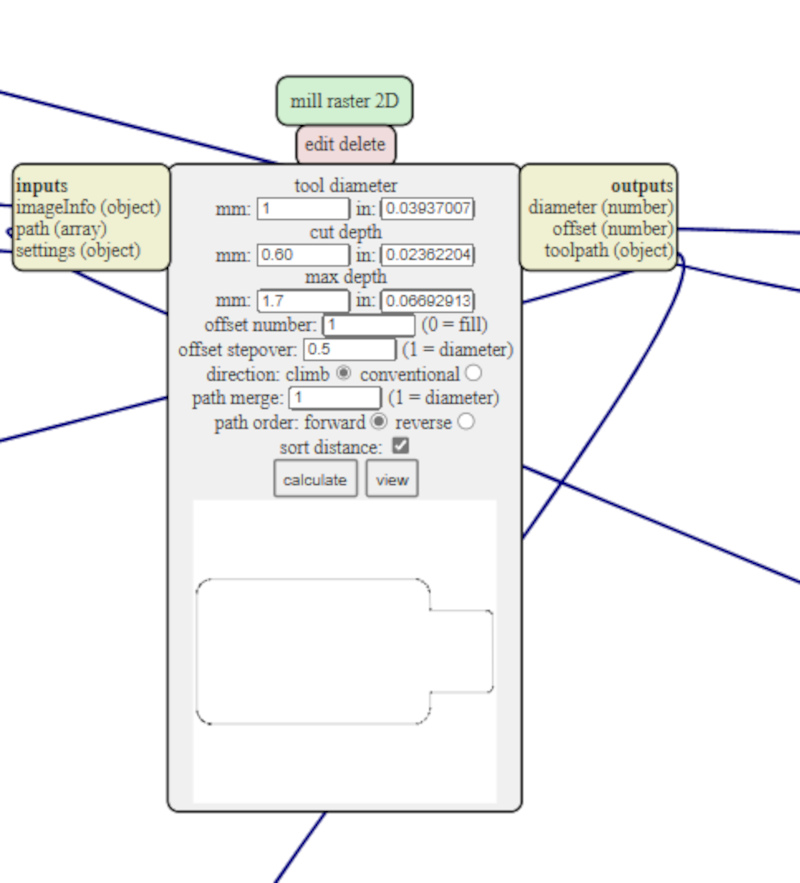
Calculate was pressed in mill raster 2D module. The resulting file was saved for cutting the outlines later. The toolpath was displayed and visually inspected. The toolpath for cutting the outlines is shown below.
Milling the board
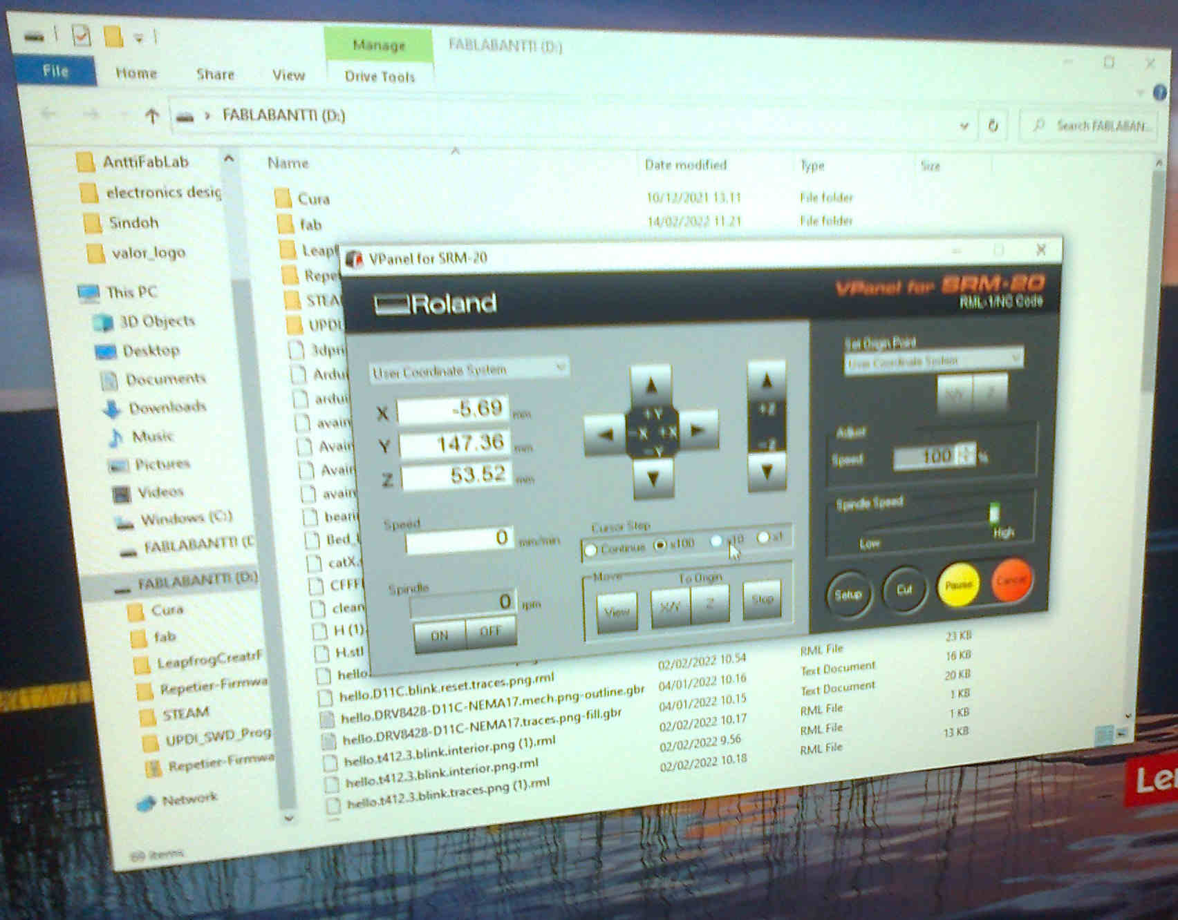
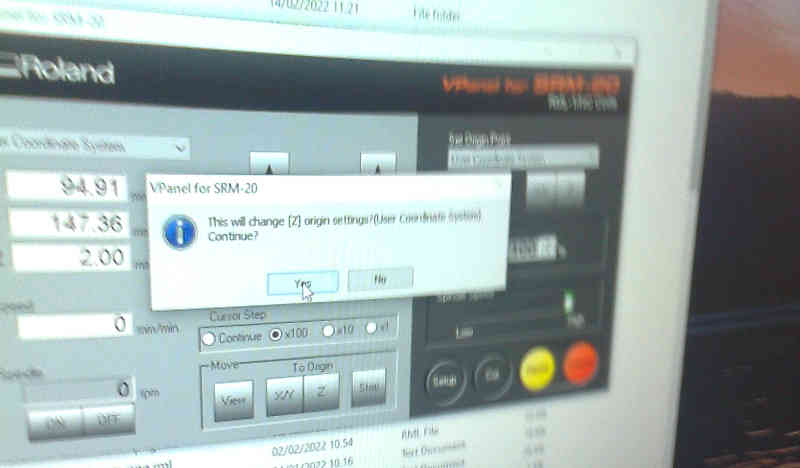
The SRM-20 was controlled by Vpanel program.
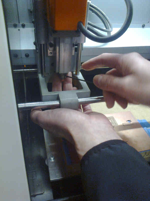
The bit was installed by hand.
The bit must be fastened by a specific tool.
If the machine is open, none of the controls will work. It is important to operate the door correctly.
The milling bit was moved to area where there was enough room for the bit. There was move to origo for coorinate axis and x/y button.
It was important to check the height and the different bits may require different settings. Checking the z-coordinate outside the milling area is important, because the moving head will break the bit and scratch the board if it moves over the object too low. When the Z-coordinate was checked on the safe spot, the bit was moved to selected x/y origo. The origo can be set separately from z-origo. This is important, because different heads requiring different settings for Z can and in this case will be used in milling or cutting the board.
When X and Y coordinates are moved to the beginning point of the milling, the door was opened, special tool was used to lower the tip of the milling bit on the top of the board. This must be done carefully in order to keep the bit in one piece. Dropping the hard tool probably will break it. The bit must be fastened then again and the z-coordinate zeroed after closing the hatch. The special tool must be returned to its place.
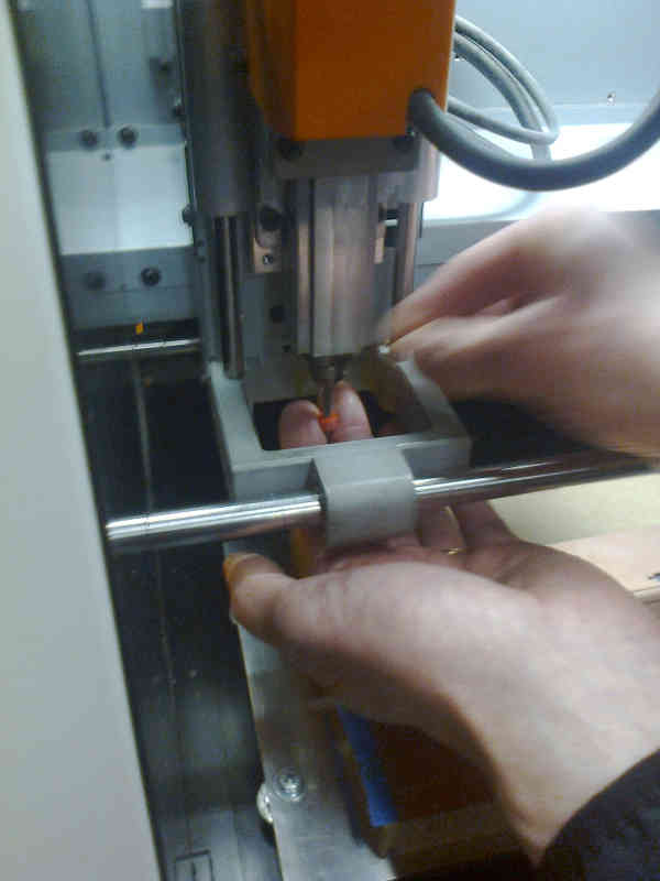
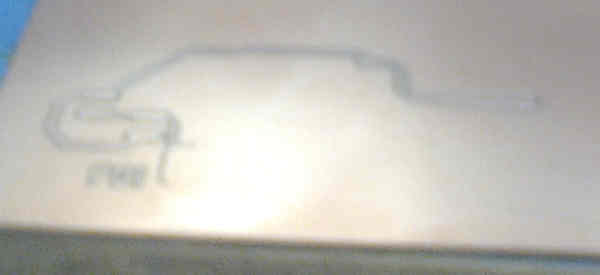
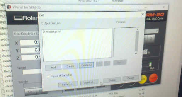
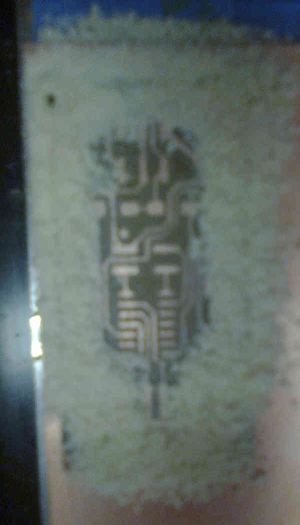
The first milling file to run was traces.rml. Orange mill bit was used. It contained the information for cutting the traced for the board. After reading the instructions file, Cutting was initiated by pressing the Cut button.
The traces were milled with a V-bit (0.2 mm). The depth of the milling had to be adjusted. It is possible to deepen the cut progressively until enough copper is milled retaining the x and y settings of the mill.
Example of the traces milled.
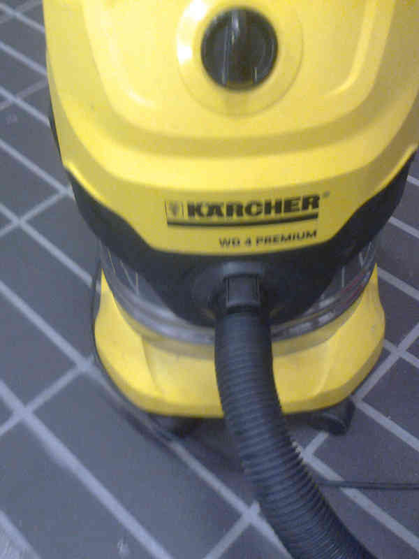
The dust was removed with a vacuum cleaner.
After the traces were milled, it was time to clean up the extra copper by using cleanup file (cleanup.rml). A purple milling bit was used.
 The new bit was installed and Z coordinate was adjusted accordingly. (1 mm end mill).
Then the cleanup was initiatized and the special tool was used for removing the dust. After adjustments, result was quite nice.
After the cleanup, outline milling file was loaded.
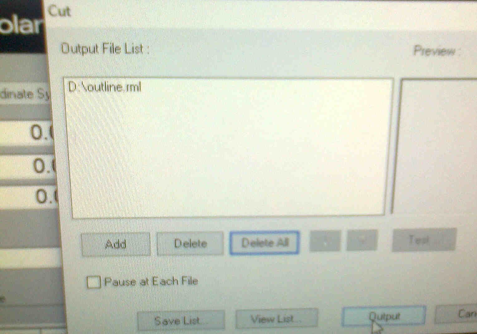
This time the installed contour milling bit (yellow) was clearly longer than previous milling bit. adjusting the z coordinate outside the milling area, as described earlier, was really important to do before moving the bit to x/y origo. The risk for breaking the bit was real. The cutting of the board was intitialized by using the .rml file previously created for cutting.
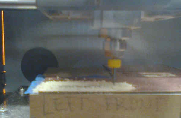
Cutting seemed to be worked and the cutted board was still firmly fasteded to the blue Scotch tape.
A vacuum cleaner was used again and the circuit board was removed with a screwdriver.
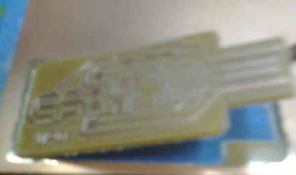
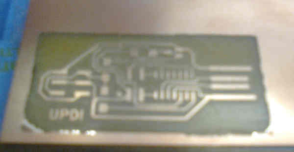
Closer observation showed that the circuit board lookes just fine.
The milling bit was removed and the machine was cleaneed.
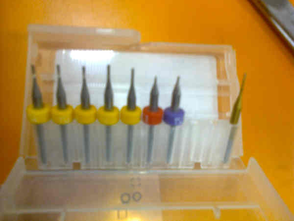
Here is a view to the milling bits used in the process.
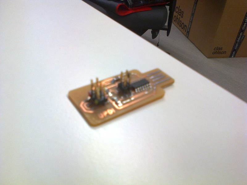
Soldering the components
The component were collected and soldered. The components included one ic, two caps, 3.3V voltage regulator, one capacitor, two resistors and two connectors. The components were soldered under magnifying lens using traditional soldering tools. The wire included flux.
The solder wire was too thick for the purpose. I managed to do the job by adding too much solder in order to get enough flux. Then I removed the extra material with copper sock. This left enough flux on the board and the extra material was gone.
After soldering the board I washed it under water and brushed the extra flux off with isopropylalcohol. I inspected the board under magnifying glass for short circuits.
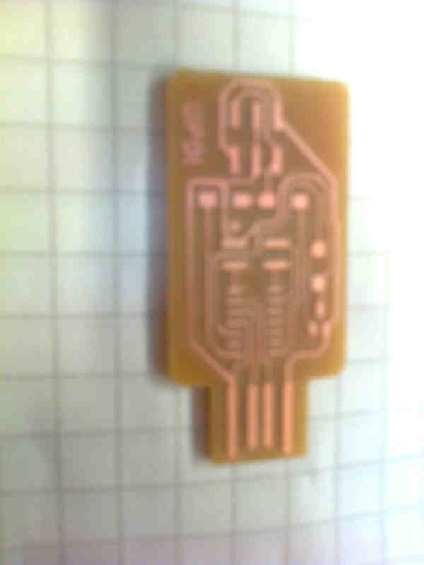
The populated board is shown below.
Programming the device.
Before programming the device was checked against shorts. None was found and the resistance values were nominal. The device was programmed in Instructor’s laptop for test purposes The stick was detected after the programming and gave correct responses in programmer. It apperas to be working. I also checked the stick in Ubuntu and lsusb showed the device.
I re-programmed the device. The programming of the USB programmer is covered in the Week 09 Documentation.
What did I learn?
Well, I learned how to mill a small circuit board. I learned, how important it is to make sure that the board is on level. I learned how to program a programmer. I soldered the components to a circuit board, but I actually have done it before.