Week 6:
Electronics Design
This week looks promising, I won't say what motivates me, but I think I finally have the opportunity to learn about real electronics. During week 4 we learned how to manufacture but not understand how PCBs work.

I think it will be the first time in my life that I can translate my electronic designs into reality. In some projects that I have worked on, I was able to design the systems, but they were far from being manufactured.
This week I hope I can learn a lot about electronics. I believe that electronics, although not a direct part of product design, is an additional element of enormous interest. Personally he loves lighting and many times I have found myself in front of great ideas, which due to lack of knowledge in programming and electronics I have not been able to do.
The three assignments for this week are:
Group assignment:
• Use the test equipment in your lab to observe the operation of a microcontroller circuit board.
Individual assignment:
• Redraw an echo hello-world board.
• Add (at least) a button and LED (with current-limiting resistor).
• Check the design rules, make it, and test it.
• Extra credit: simulate its operation.
Group Assignment
For this week's group assignment we have taken advantage of one of the clubs offered by our Lab. Last week we started working, as an additional task, on a website powered by sunlight. We think we can use the assignment to learn about microcontrollers, and more specifically about the ones we are using in the solar server.
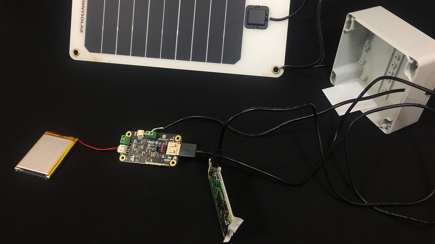
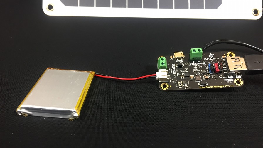
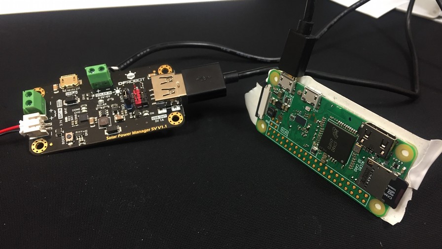
The hardware-level solar web is made up of a solar panel, a Li-Po battery, a power manager and a Rapsberry Pi Zero. We will focus our efforts on understanding the operation of the power manager.
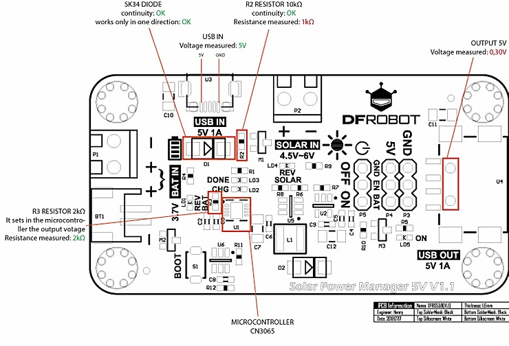
The first thing we did was find all the specifications, datasheets and possible diagrams on the manufacturer's website. In the following link you will find all the datasheets that make up this PCB intended for power management.
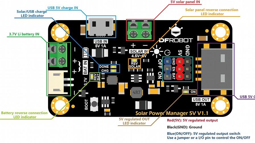
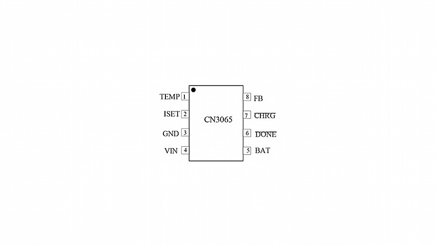
The next step was to find out which microcontrollers had soldiers and find the maximum information about them. When we had all the information we decided to focus on the CN3065. This is responsible for automatically directing the current and the system that surrounds it prevents reverse connections from occurring.
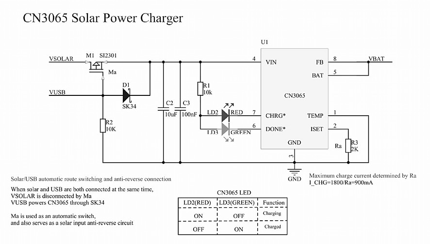
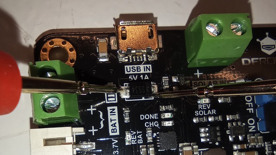
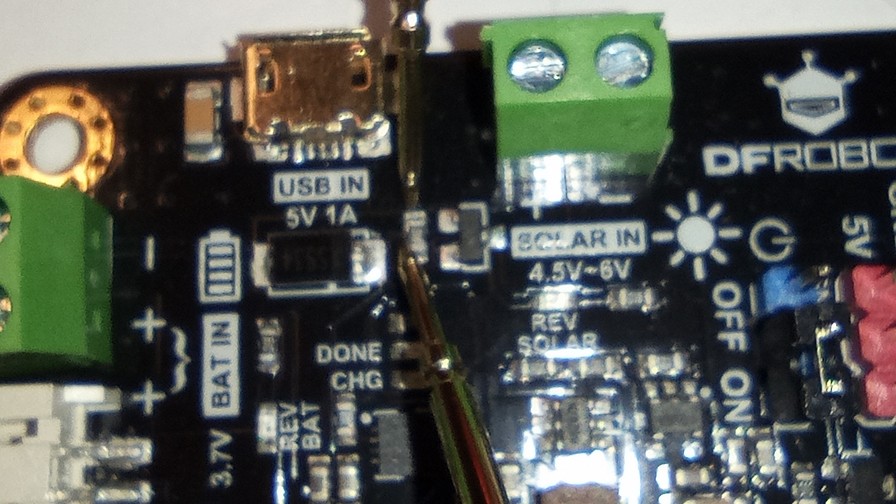
What we did then was understand the components it interacts with, but during that week something broke. We thought it would be great to look for the broken component, as a test for the web. But also as an excuse to use the multimeter and test the data that it can give us from the PCB.
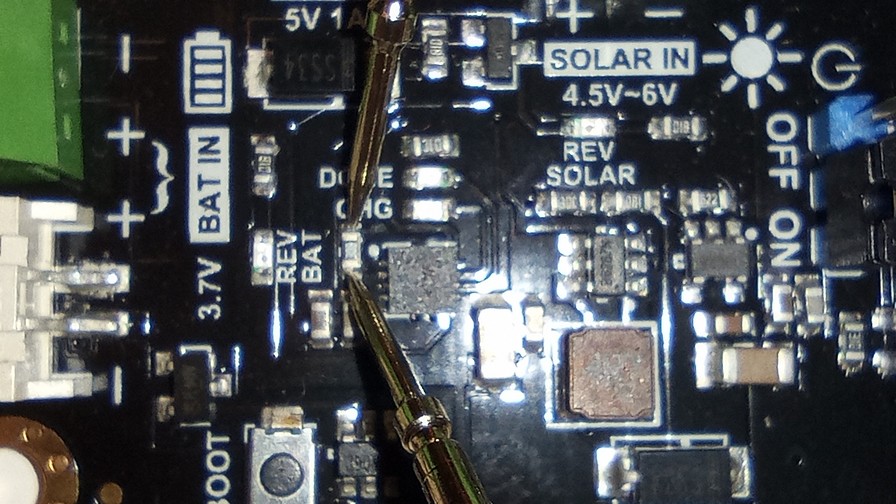
After many attempts and mistakes, we couldn't find the source of the problem, so Oscar our instructor gave us another power manager. Even so, we made the following graph as a conclusion to our analysis.
Individual Assignment
For the individual assigment I have thought of trying to be as efficient as possible. My knowledge of electronics is very limited at the moment and I think it is better to keep a low profile for now, but understand the basics of operation.
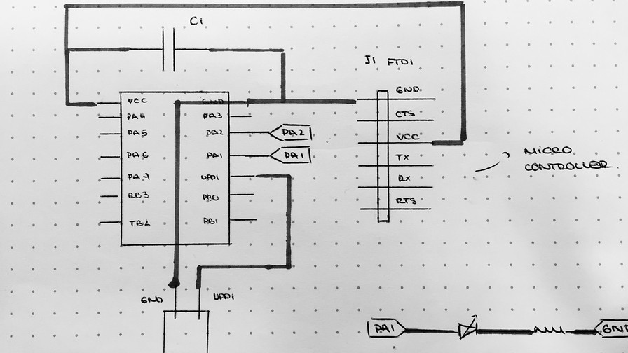
For this I am going to try to create a PCB that is useful to me with the ones we created during week 4. Those boards should allow us to work together with the one I made this week. If I'm not wrong making a simple hello board with a microcontroller, I will be able to solve some general doubts that I still have.
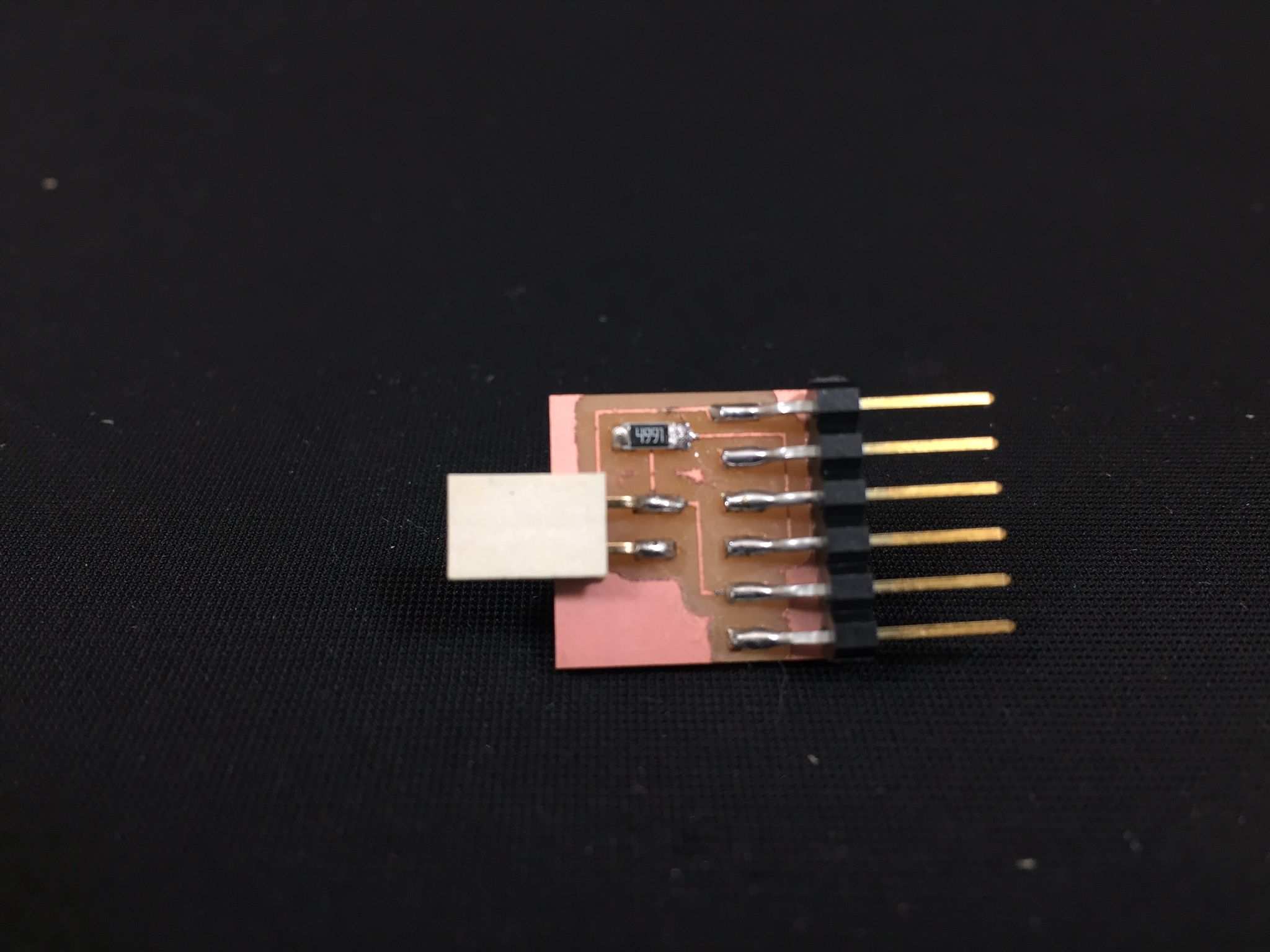
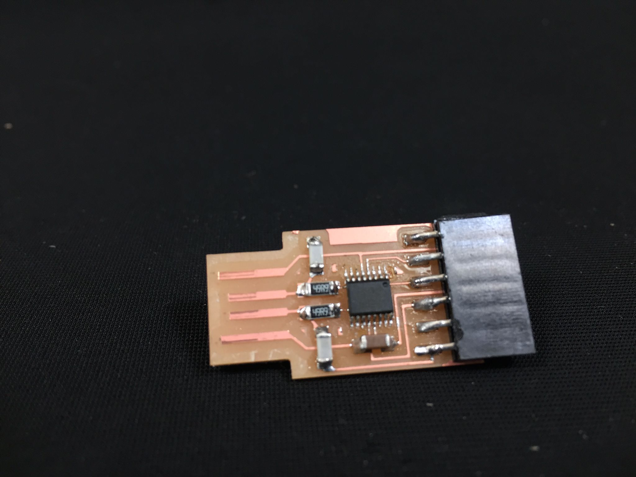
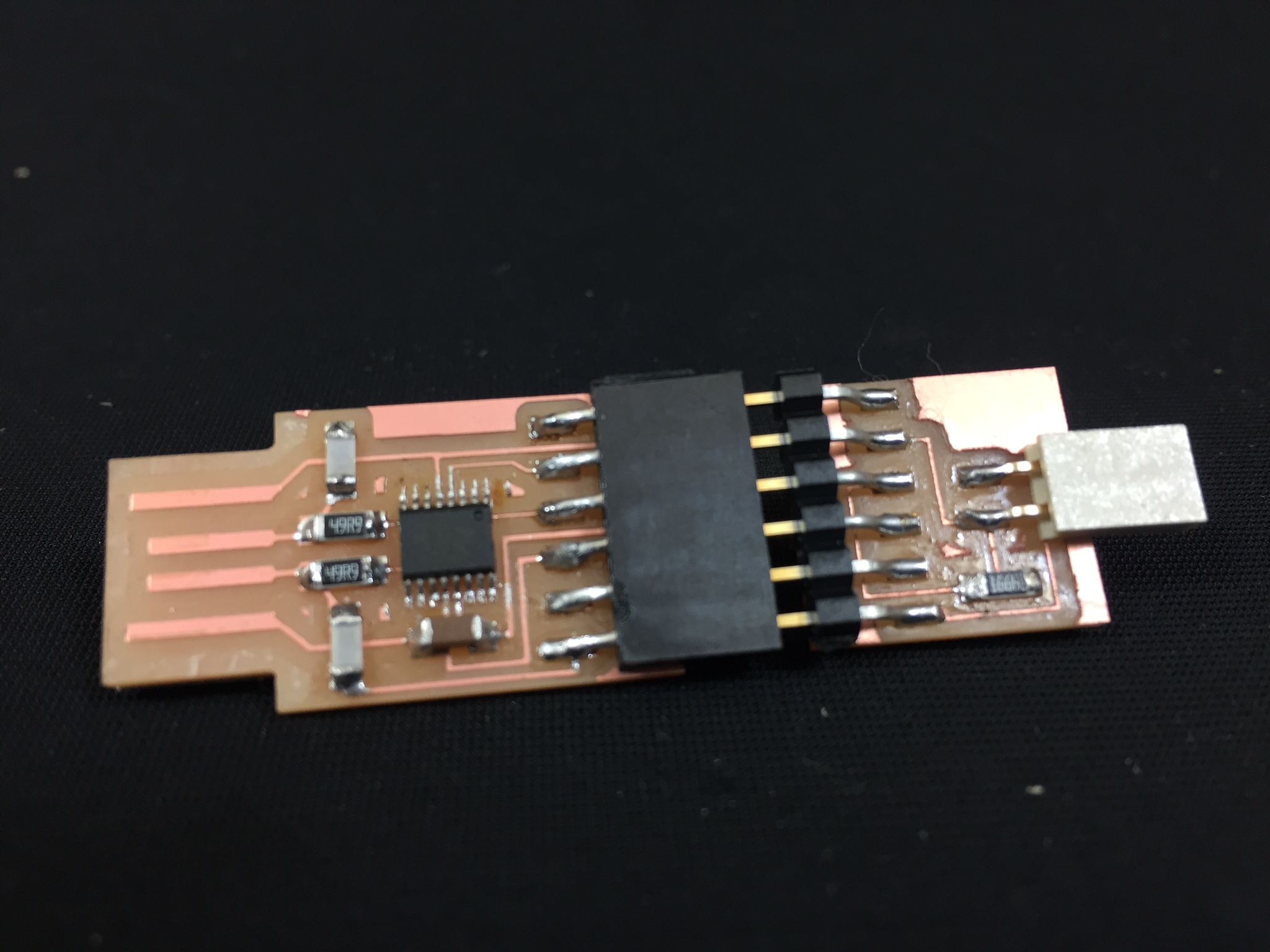
Last week's circuit boards were a UTDI and an FTDI which I believe are used to configure other microcontrolled circuits. The following images show the work from week 4, to create a foundation to work on.
For my final project, I want to work with various inputs, and try to generate outputs that move motors and dim lights. I am not sure that with the plate that I will do this week I can do that, but I think that the level of difficulty will be low enough to understand what I am doing.
Talking to Josep, one of my instructors, he recommended me the following workflow:
- Work with the ATtiny1614
- Start with the hello board that includes it
- Work in KiCad throughout the design process
- Add a button as input
- Add an LED as an output
- Make the physical board
- Work with the microcontroller and program something
As they have experience in the subject, I will follow the workflow trying to understand the maximum possible concepts. Let's do it!
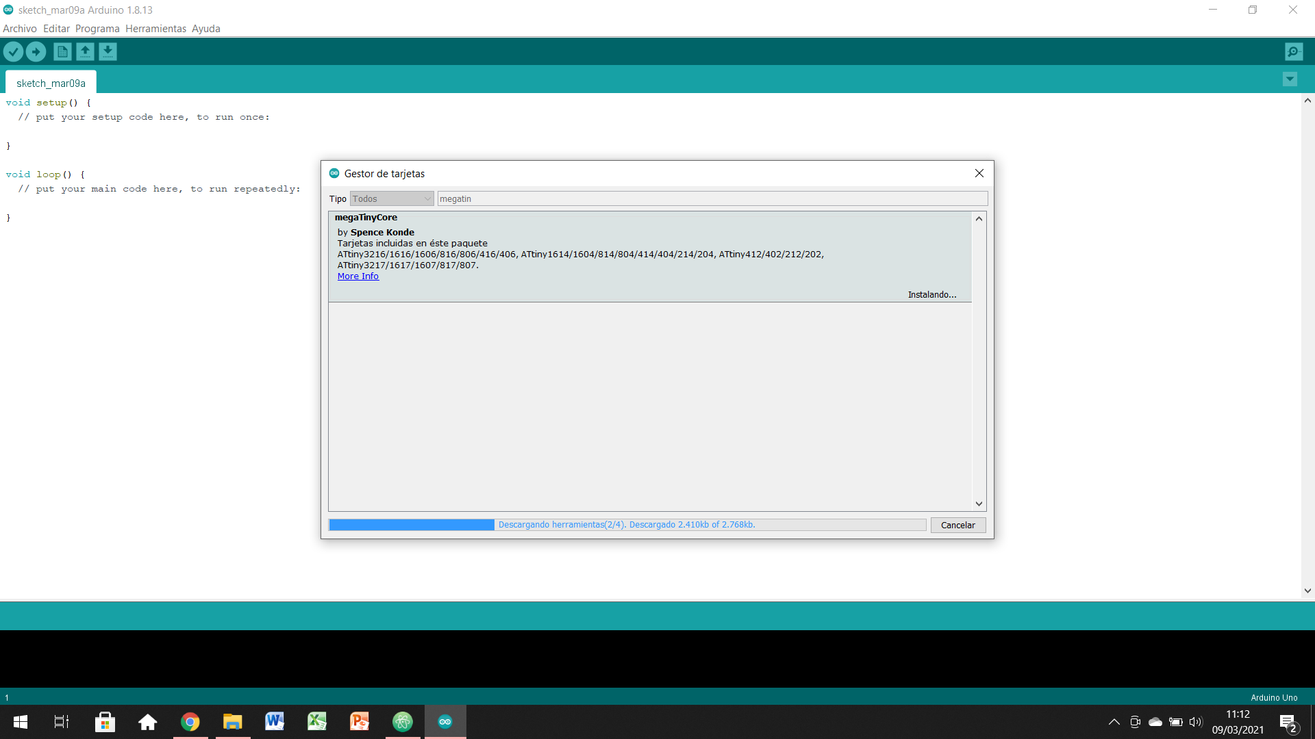
Download and understand the Hello-Board for ATtiny1614
The first thing to do was to find out which of the hello boards was the most suitable for me. For that, I discussed the simplest but adequate microcontroller with Josep. He recommended the ATtiny1614 for its versatility, but also because it is easy to use and weld.
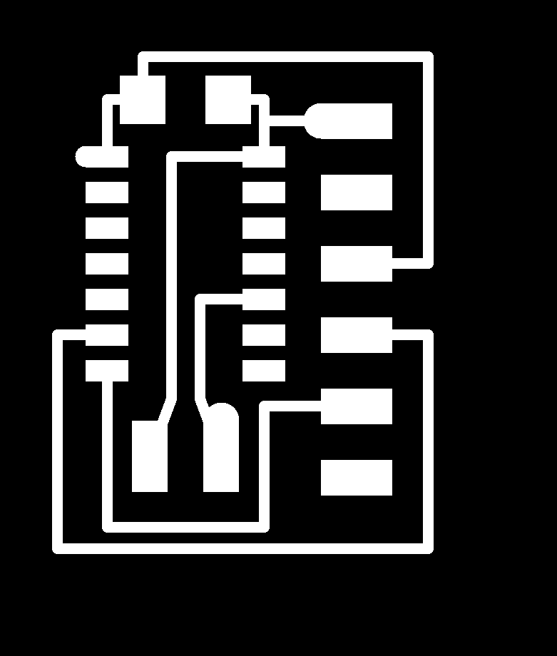
Once the operation was understood and the most basic way to add the LED (output) and the button (input), it was time to draw the system on paper, to understand it better. Since my background is engineering, I feel more comfortable working with a piece of paper first.
Design by hand the PCB
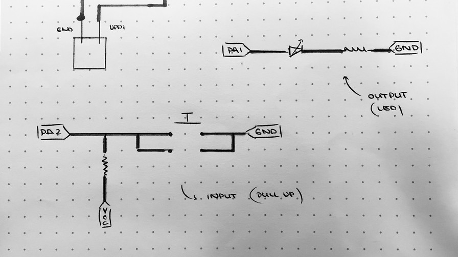
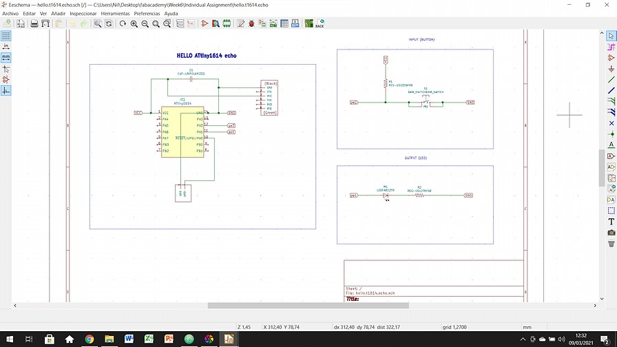
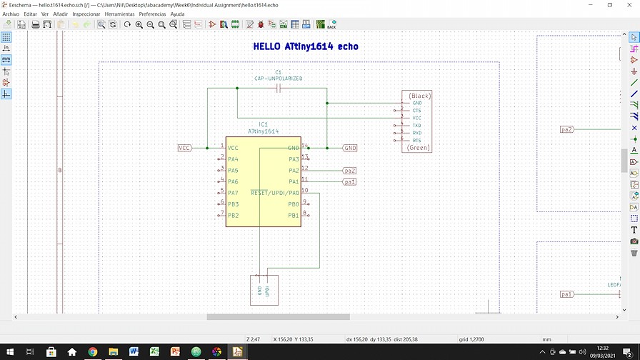
Working on paper helps me understand the connections between the components and makes my work easier and then takes it to the KiCad schematic. As you can see in the images, I add to the Hello Board, a pull up button to have a simple inout and as an output, a green LED protected by a resistor.
To decide which pins I need to use to redraw my board, I use the pinout scheme of the ATTiny1614 microcontroller.
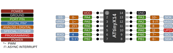
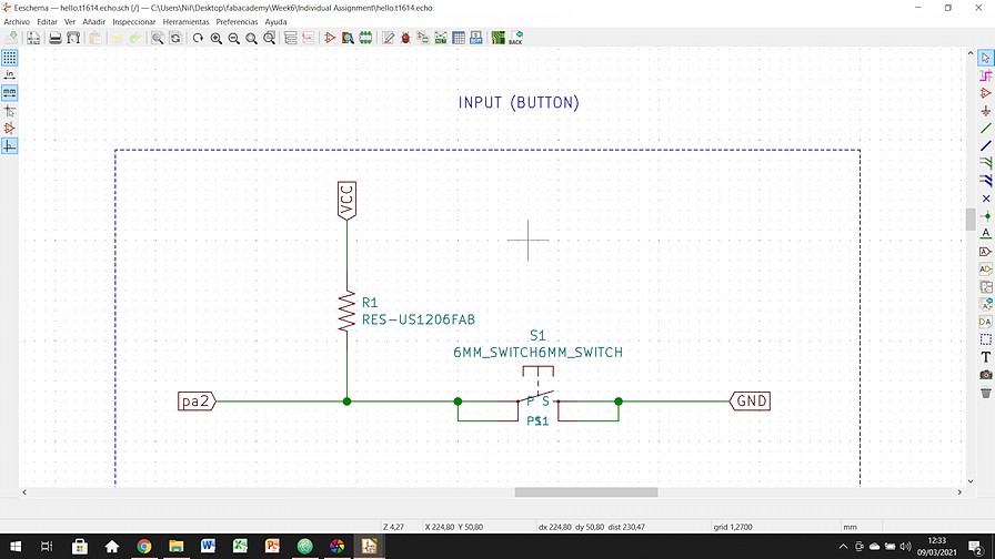
As you can see, for the button I use pin 9 and I will use it as INPUT. That pin can work as input or output so it's convenient for me for what I need to do.
In addition to the button, I put a very high value resistor to generate a pullup between the button and the pin. That allows me to get a clear signal between 1 and 0 or HIGH and LOW.
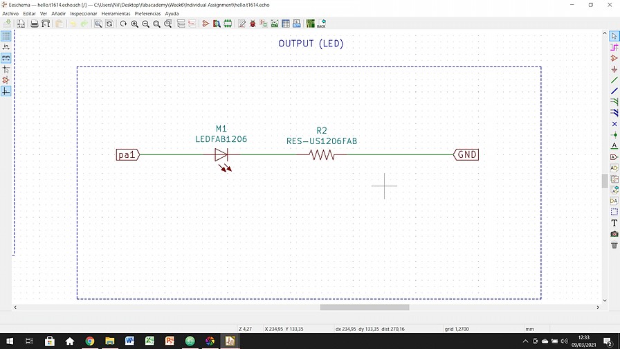
On the other hand I connect the LED to pin 8 that I will use as OUPUT. In the same way as 9, it can work as input and output so it's convenient for me again.
In addition to the LED, and as it will always be necessary when using one, I must put a resistor that protects the LED.
DRC: Design Rule Checking
I'm not familiar with these design rules to keep in mind but I think a definition is a good way to understand them. Quoting literal:
"Design rules are a series of parameters provided by semiconductor manufacturers that enable the designer to verify the correctness of a mask set. Design rules are specific to a particular semiconductor manufacturing process. A design rule set specifies certain geometric and connectivity restrictions to ensure sufficient margins to account for variability in semiconductor manufacturing processes, so as to ensure that most of the parts work correctly."
The three basic rules, and in which I will be able to pay attention for the designs from here on are:
- Width (100-400nm): specifies the minimum width of any shape in the design
- Spacing (100-400nm): specifies the minimum spacing of any shape in the design
- Enclosure (10 nm): specify that an object of one type, such as a contact or via, must be covered, with some additional margin, by a metal layer
These rules apply when you design the PCB at the geometry and layout level, so they will be taken into account in the next step. Basically to ensure that there are no shorts or problems related to connectivity and electricity.
These restrictions do not seriously affect my projects due to the measures that my tools allow me to carry out. For now I think it is possible to understand how to design and how to make PCBs to later start reducing the sizes, taking into account these design rules.
Workflow in Kicad
It was the first time that I have used the Kicad software, but I admit that I found it tremendously useful. Before to simulate circuits, I did not have any tool that allowed me to work with electronic components so clearly. The user experience is not very good, because the software is rigid at times, but the power is very good.
The process to develop a PCB consists of making the connections in the form of a schematic, and then passing it to the manufacturing module. The first step is perhaps the most complex. Making drawings of a PCB is something that I had never done but in a few minutes it was solved.
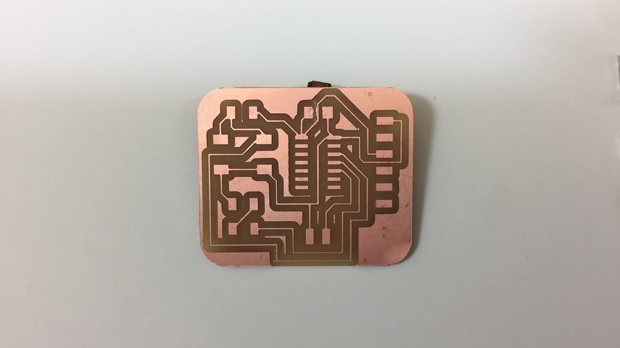
Once the schematic was done, it was time to work on the footprint module. Each component appears with its markings on the PCB and the wiring system is intuitive but not straightforward. After some horrible and too big attempts I got to the schematic that you can see in the images below.
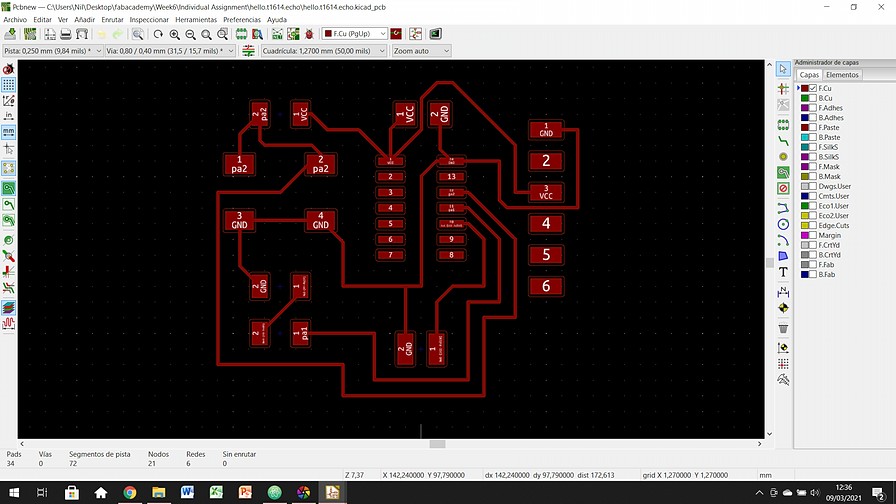
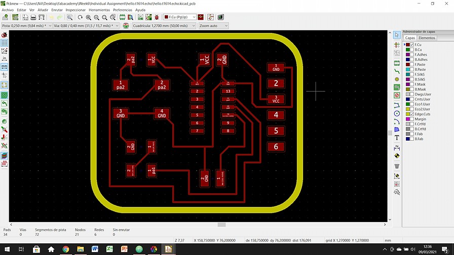
Looking for the best non-automatic alternative, I think I have achieved a pretty good result and I think it will be easy to weld by hand. The PCB is about 2.5x2.9mm, which I think is not bad at all.
The last step was to export the PCB documents in .svg format, so that they could be processed later with Illustrator or Inkscape. The saving options are not complex, but paying attention is important so that you export them in monochrome and all unified in the same file.
Prepare the files in Illustrator
To generate the pngs to take to ModsProject, it is necessary to treat the documents a bit with a vector rendering program. In my case, I have experience with Illustrator so the decision was clear. It gives a few more problems than Inkscape, but I feel more comfortable.
The process with Illustrator consists of inverting the colors of the .svg so that the machine understands that the white areas should be preserved. It is important that both black and white are as saturated as possible so that the software understands the border between the two.
Finally the files that I got are the two images that you have below. The first shows the PCB traces and the second shows the inside for the 1/32 "bit that will make the external cut.

Create the g-code files
ModsProject is no longer an unknown because during week 4 we fought enough haha. I load the pngs and configure the parameters with the same optimal values that we found during that week. Those values are: (insert data board).
Finally, it is only necessary to upload the documents in the IAAC cloud and prepare the origins and documents on the Roland SRM-20. Now I just have to wait for the machine to finish milling.


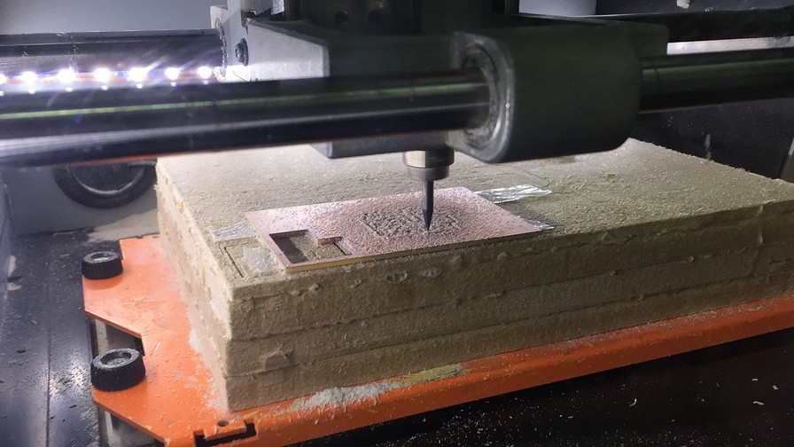
Milling
The milling process was not easy. In a first attempt the png files were not well done and the bit did not fit between the microcontroller pads. Making a few small changes to the thickness in Illustrator, there was no problem.
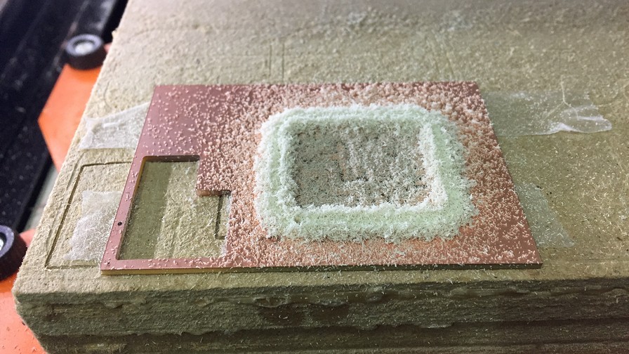
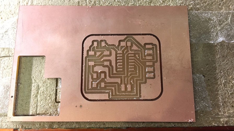
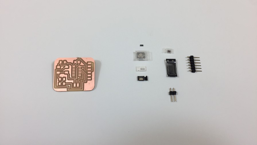
Clean and prepare for soldering
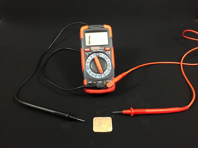
I cleaned the contacts and tracks with a little alcohol and a cotton swab. Everything seemed to be correct and after checking with the multimeter if there was continuity in all the tracks I started soldering.
Soldering
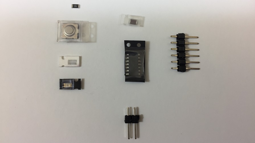
This microcontroller has been a thousand times easier to weld than those of the UPDI and FTDI. The pins are larger and are much further apart from each other. I will not say that it is simple, but comparatively it is much more so. Here you have some images to undestand the way easier soldering I came across this time.
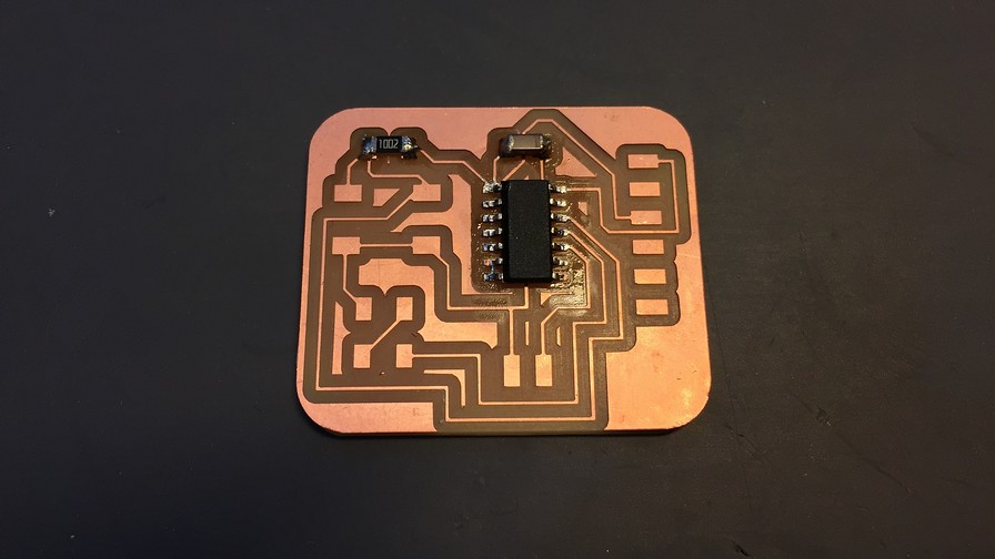
As you can see in the images below, I prepared a layout so that there were no errors during the welding process. I copied the PCB schematic, placing the components in their exact position.
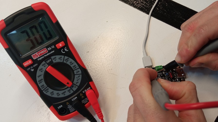
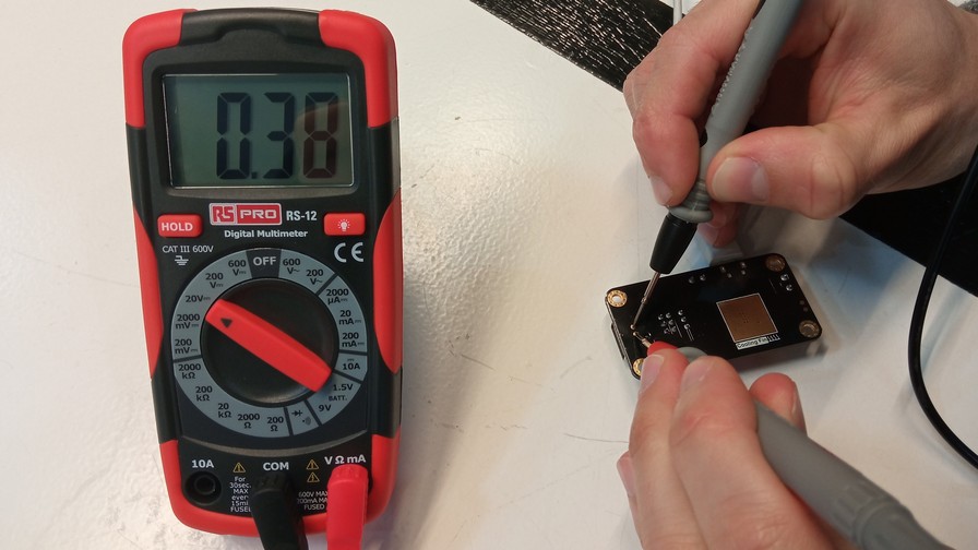
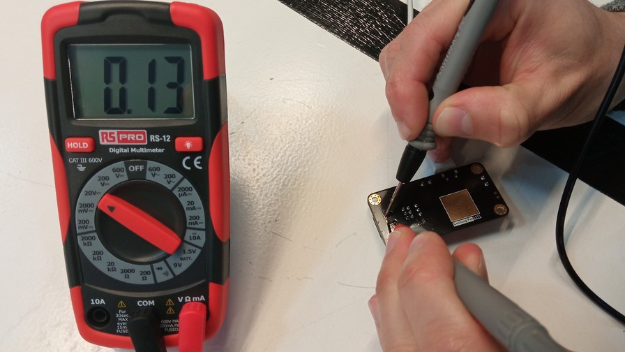
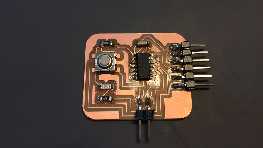
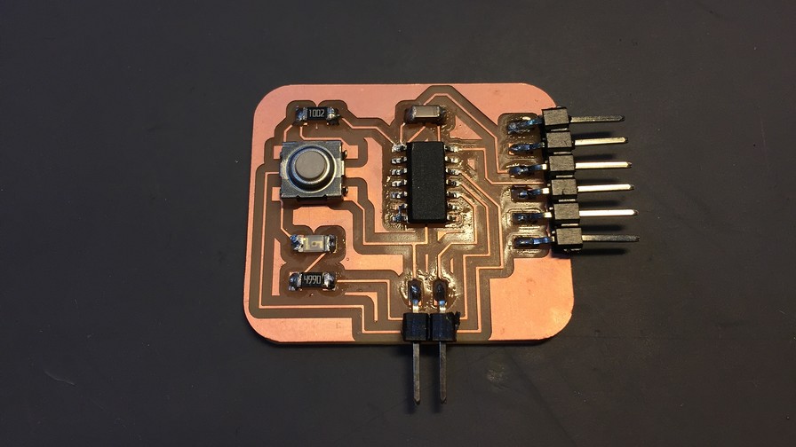
Testing
What I have done to test the PCB has been to study the continuity in all the tracks, to check that the components fulfill their function and that the button works correctly.
In order not to lengthen this point excessively, below you have a few images of how I have carried out the checks. You will also find a small table as a checklist where I was writing down the different tasks and their results.
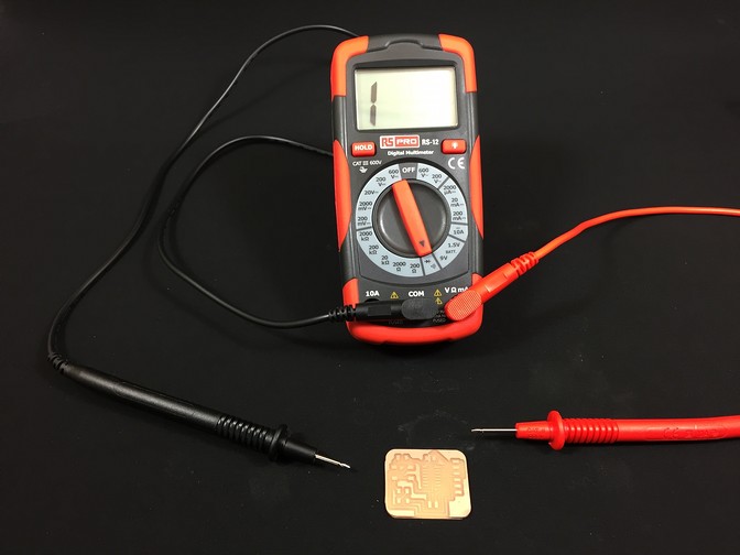
| Task | Expected | Value |
|---|---|---|
| Continuity tracks | multimeter beep | ok |
| Continuity pads | multimeter beep | ok |
| All GND connected | multimeter beep | ok |
| FTDI and UPDI input | multimeter beep | ok |
| Resistor values | 10k and 499 Ohms | 9,99KOhms / 499Ohms |
| LED and Button polarity | Visual check for LED and multimeter beep for button | LED /ok Press button / Multimeter beep |
Since all the multimeter and visual checks are positive, I think this week's weekly assignment has been more than fulfilled. More considering that I had rarely had such an experience with electronic components.
Programming
To program the board and check if it is working correctly, I followed the wonderful guide that Adrian Torres made during his Fab Academy in 2020. Within his website there is the Adrianino tab in which he explains the programming processes very well.
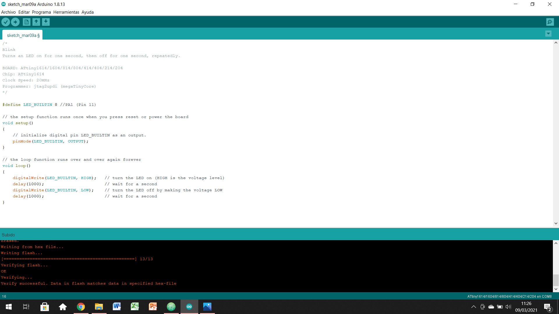
When the program was already uploaded to the microcontroller the LED was not lighting up. After looking at it for a while, I realized that I soldered the LED in the opposite direction. Logically when I checked with a multimeter it worked, but I did not realize the polarity. It was time to desolder, turn it 180º and solder again.
Here is the link to the programming Arduino website, where I got the lines of code.
	/*
	  Blink
	  Turns an LED on for one second, then off for one second, repeatedly.

	  BOARD: ATtiny1614/1604/814/804/414/404/214/204
	  Chip: ATtiny1614
	  Clock Speed: 20MHz
	  Programmer: jtag2updi (megaTinyCore)
	*/

	#define LED_BUILTIN 2 //PA1 (Pin 11)

	// the setup function runs once when you press reset or power the board
	void setup()
	{
	  // initialize digital pin LED_BUILTIN as an output.
	  pinMode(LED_BUILTIN, OUTPUT);
	}

	// the loop function runs over and over again forever
	void loop()
	{
	  digitalWrite(LED_BUILTIN, HIGH);   // turn the LED on (HIGH is the voltage level)
	  delay(100);                       // wait for a second
	  digitalWrite(LED_BUILTIN, LOW);    // turn the LED off by making the voltage LOW
	  delay(100);                       // wait for a second
	}
I simply plugged the power in and it worked !!!! The upload had worked fine, but the LED was backwards. This time everything worked perfectly and it has started to blink.
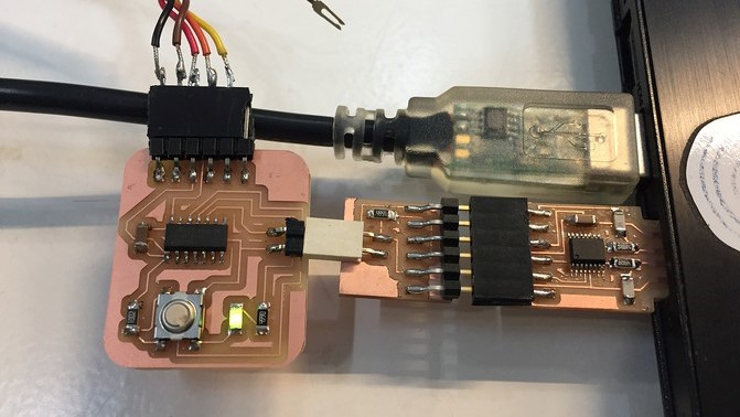
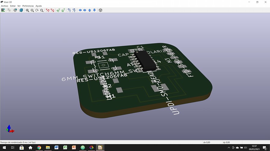
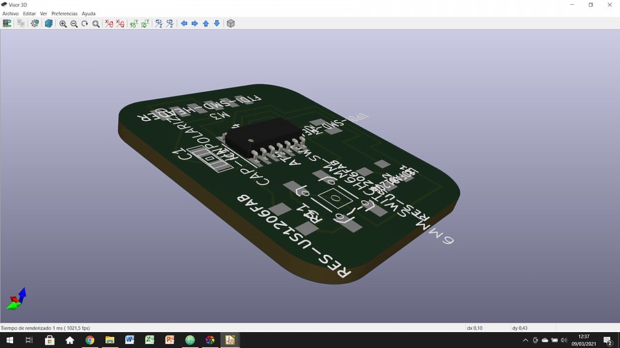
Hero Shots
These images an videos that you have below make me very happy. I begin to have the feeling that the electronics skills that I am learning will allow me to carry out much more robust projects than to date.
I think being able to do electronics from manufacturing to programming and testing is a great tool for design engineers. It is interesting to be able to take into account the electronics of your product during the design process.
Links haven't been working for the last couple weeks. Here is the link to it.
Links haven't been working for the last couple weeks. Here is the link to it.
Here is the link to the original files for individual assignment.
Original Files
Link to Original files from this week.
What to improve for next assignments?
The worst part of this week has been time management. The work is beginning to be difficult to reconcile with the FabAcademy. I waste many hours moving from one place to another (I live far from the Lab), which results in me having to decide between: sacrificing documentation for the web or doing simpler projects. I am at a point where it is being impossible for me to work in spirals. I have to learn the most from the few attempts I can make.
What to keep an eye on during week 6?
· Time management as usual.
· Even though it goes against my principles, I have to start working on the weekends.
· Try to somehow reduce commute or find other alternatives.