7. Electronics design
This week I learn the PCB designing process and I was introduced to the diferent tools and softwares that make that process possible.
Group Assigment
Individual Assignment
Eagle - electronics design software

Eagle was the proposed software for this assigment. It was not to difficult to learn to use it.
Electronics design Workflow
The first thing I did was to copy the Fab library into Eagle’s library.
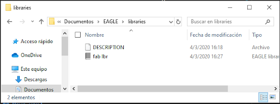
After that I activate the library into the software:

Before starting with the circuit design software I choose a Hello World board to redraw it and I added a termistor and a 150 resistor.
Hello Wold’s BOM:
| Part | Value | Device | Package | Description | |
| C1 | 1uF | C-EUC1206 | C1206 | CAPACITOR, European symbol | |
| IC1 | ATTINY44-SSU | ATTINY44-SSU | SOIC14 | ||
| J2 | FTDI-SMD-HEADER | FTDI-SMD-HEADER | 1X06SMD | ||
| R1 | 10k | R-EU_M1206 | M1206 | RESISTOR, European symbol | |
| R2 | 150 | RES-US1206FAB | R1206FAB | Resistor (US Symbol) | |
| R3 | 10k | RES-US1206FAB | R1206FAB | Resistor (US Symbol) | |
| R4 | 0 | RES-US1206FAB | R1206FAB | Resistor (US Symbol) | |
| S1 | 6MM_SWITCH6MM_SWITCH | 6MM_SWITCH | OMRON SWITCH | ||
| U$1 | LEDFAB1206 | LEDFAB1206 | LED1206FAB | LED | |
| U$2 | TERM-1X03'-FABLAB' | TERM-1X03'-FABLAB' | ED555DS-3DS | 3.5mm terminal block, 3 positions ED555-3DS as found in the fablab inventory. | |
| U$3 | AVRISPSMD | AVRISPSMD | 2X03SMD | ||
| XTAL1 | 20MHZ | RESONATOR | EFOBM |
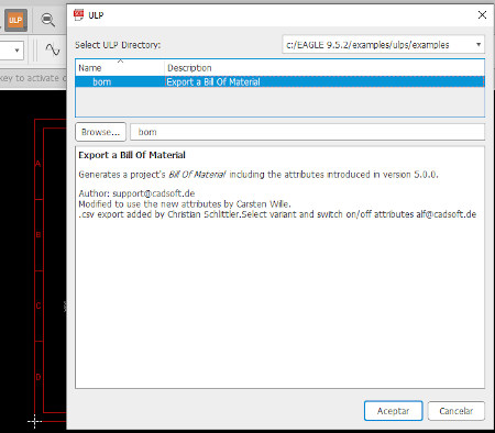
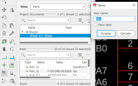
To find my board’s BOM:
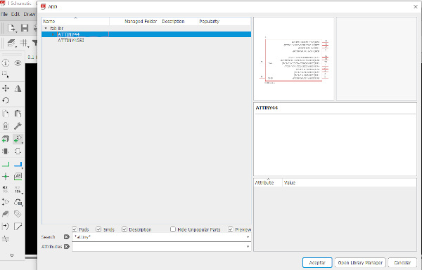
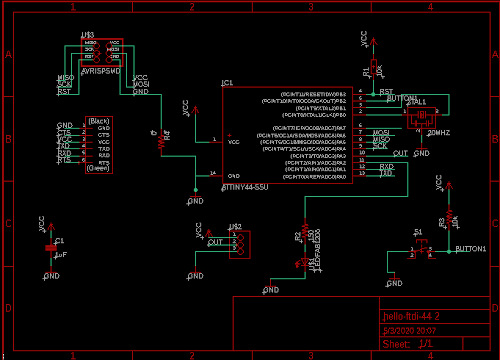
Once that done I could start to design my electronic circuits. First I had to import the components into the work area.
There are some indispensable components in a PCB:
- Microcontroller
- capacitor (is like a filter between GND and VCC)
- oscilator (determines the pulse or the speed )
- 10k resistor to RST (prevent from reseting the micrcontroller)
Besides theses, all inputs and outputs has to be installed with other components following their datasheet’s indications.
I learned how to connect and move components.

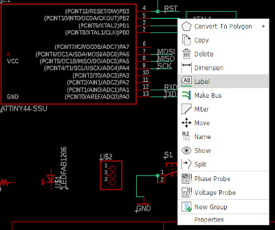
Creating labels to name pins and attributing values to components. Here is important to know that 2 pins named by the same are automatically connected even if ther is not a visual circuit between them. Is a good method to avoid cross circuits.
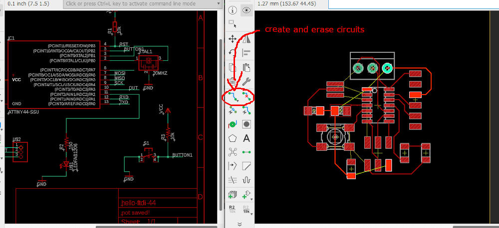
Then we pass to the next part, the circuits design. For that We click in the green BDR button:

That action bring us to the following scenario:

Here we can start to design, understanding that all the yellow lines have to disappear by creating connections between the pins. The circuits width recommended was 0.4mm or 24mil. A reference of a correct line width is the microcontrollers pin’s soldering zone.
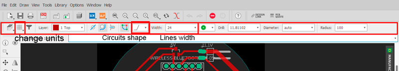
We use the basical setting parameters here above.
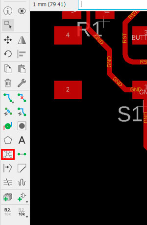
Here there is a tool that helps a lot. The”Ratsnest” button serves to update the circuits so it show the new optimal connections in function of the components location. It’s important to click on it after every component movement.
The result of my first design was not huge because there where some imposible o extremly complex connections to do. You can download my two first failed designs here:
So I started from scratch again. The third attempt was better, I follow a student advise about putting components around de microcontroller and creating circuits one by one just after placing the component instead of placing all the components first and creating all the circuits after, just like I’ve done before.
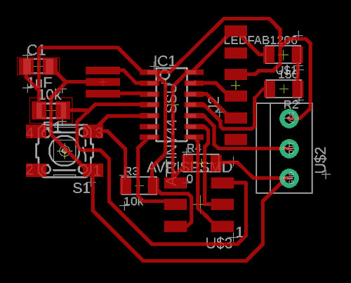
This design needed just a supplementary resistance of 0k to make a bridge. To reach this result I had to design some circuits with 0.3 mm instead of 0.4 to be able to make them pass through very small spaces.

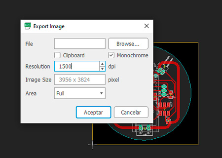
When my design was ready I exported a 2D file from this circuit board. Here the Monochrome box have to be checked.
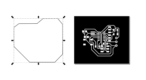
After that I designed the shape of the board in Inkscape.

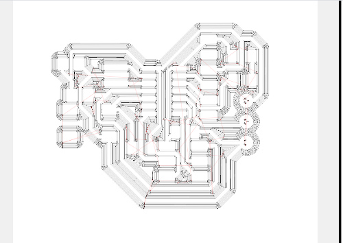
Then I opened the files in MODS and I generate the two GCodes. For that I had a problem, the toolpath was not passing between some circuits because of the tool’s diamater , so I reduced of 0.01 this setting until the toolpath shows correctly.
After I maked the autolevel process described in the Electronics production assigment.
GCodes files can be dowloaded here:
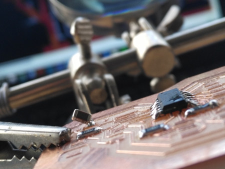
Finaly I mechanized the board in the lab’s CNC machine

After that I pass to the soldering part. I didn’t know about the position requirement of the FTDI component so I must put it vertically.

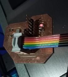
Finally I test the connection between the board and my computer and it works!

Eagle’s files can be dowloaded here:
GCodes files can be dowloaded here:
HERO SHOT
Loading a program
The program loaded was writed in Arduino:
void setup()
{
  pinMode(2,OUTPUT); //CONFIGURATION DEL PIN
  digitalWrite(2,LOW); //INICIA EL PIN EN ESTADO BAJO 0 LOGIC O 0 VOLTIOS
}
void loop()
{
  digitalWrite(2,HIGH);
  delay(1000); //esto son 1000 milisegundos = 1 segundo
  digitalWrite(2,LOW);
  delay(1000);
}
And it worked!
HERO SHOT

Conclusion
I liked this assignment because I find it incredible to be able to create a PCB from scratch. In this point (final project process) I know it is very important to consider the amount of energy and current to which the PCB will be exposed to avoid heating issues of the microcontroller or the components.
It’s important to do not abuse making the tracks pass between small spaces or leaving short spaces between lines because it increases the short circuit risk.
Resistors are consumption bridges between an output and the whole source energy to control the power distributed to the component.
Learning outcomes
- [x] Select and use software for circuit board design
- [x] Demonstrate workflows used in circuit board design
Have you?
- [x] Linked to the group assignment page
- [x] Documented what you have learned in electronics design
- [x] Explained problems and how you fixed them, if you make a board and it doesn’t work; fix the board (with jumper wires etc) until it does work.
- [x] Included original design files (Eagle, KiCad, - whatever)
- [x] Included a ‘hero shot’ of your board
- [x] Loaded a program and tested if your board works