7. Electronics design
This week I worked on my circuit board, Hellow world.
Research
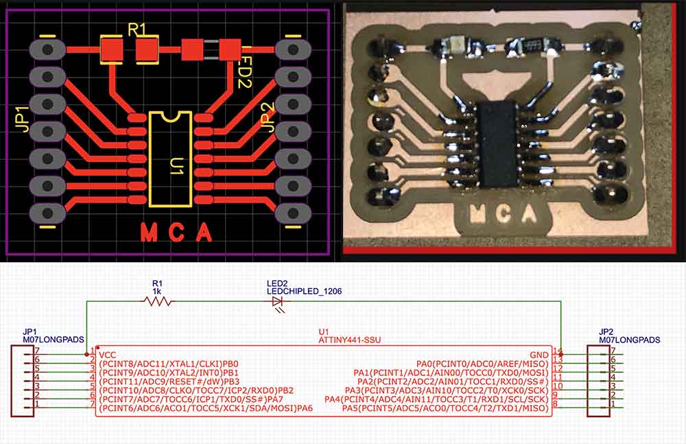
I use the EasyEDA online software but because i have a Macbook, it is preferable to use Chrome instead of Safari. First i did a practice to learn the online software EasyEda and Flatcam. I use Microcontroler ATTiny 44, two ISP, 01 resistance R1K.
First i use Easyeda to add the electronic components.
After add all the electronic components from the Library, i start with the PCB creation and to parth the different electronic components.
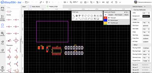
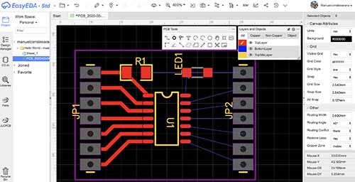
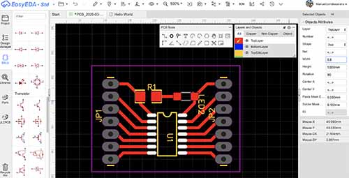
Routing the different components
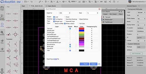
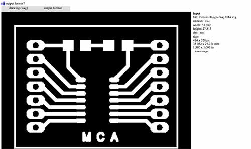
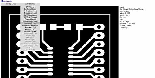
Then we use Fabmodules to prepare the schematic for the Milling machine. Here the parameters for the Milling machine, the Roland RSM 20
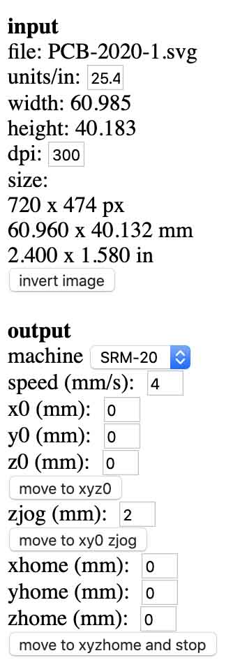
In the output milling machine SRM 20
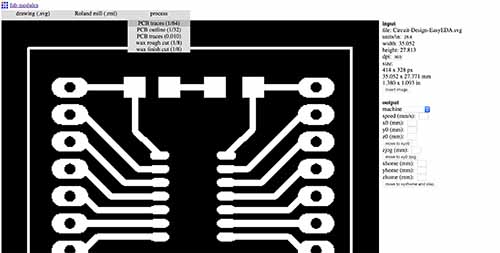
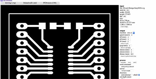
For the outline or border: PCB Outline 1/32
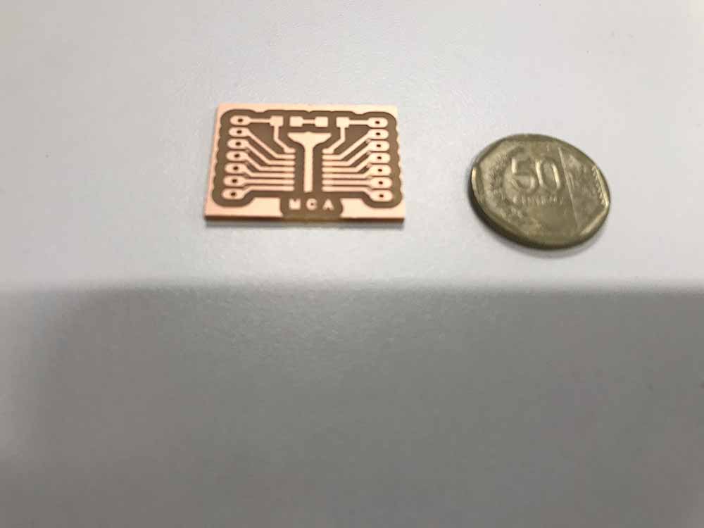
After miling: Here the circuit and a 0.50 cents coin to compare the size.
The last step is to solder all the components.
Task 1: Use the test equipment in your lab to observe the operation of a microcontroller circuit board (Group work)
We test our circuit after being programed in arduino. Giving a pulse of 5V to a LED that turns on each second and rest for a second. An oscilloscope is an Electronic laboratory instrument commonly used to display and analyze the waveform of electronic signals. In effect, the device draws a graph of the instantaneous signal voltage as a function of time.
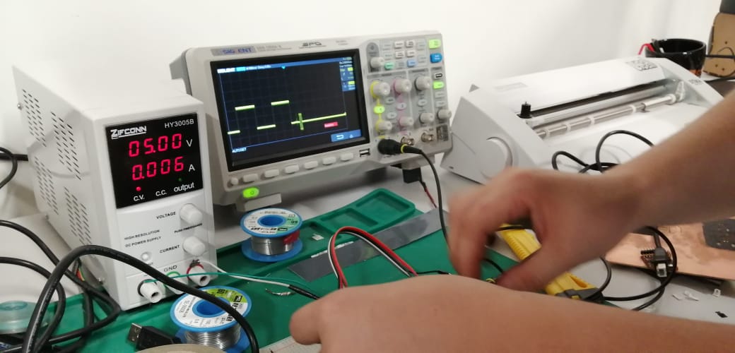
After coneecting what we saw the periodicity of the signal showing lines either in an upper position nor a lower position.
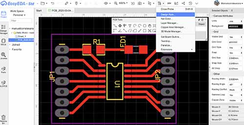
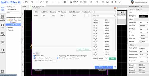
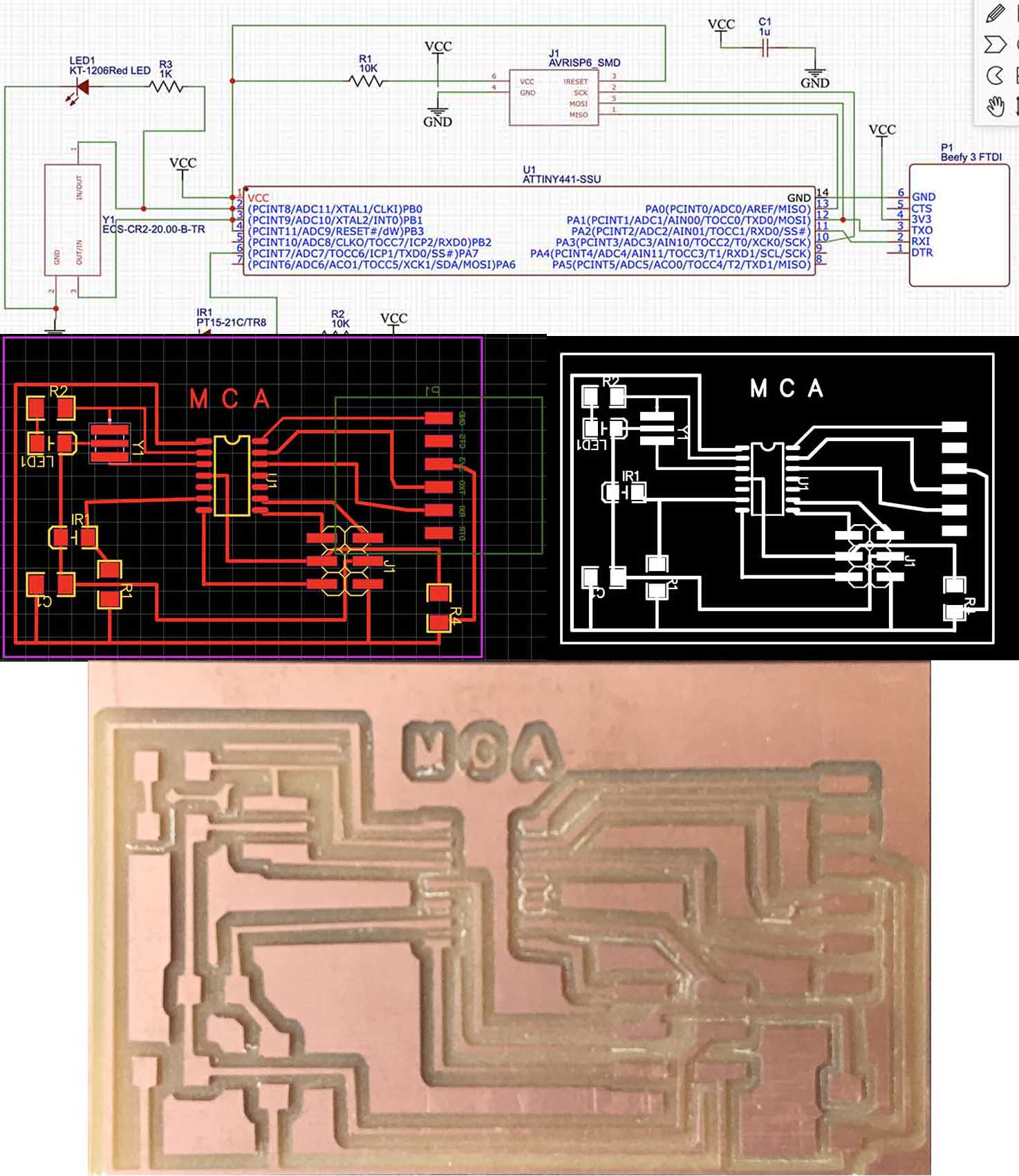
Task 2: Redraw an echo hello-world board, add (at least) a button and LED (with Current-limiting resistor), check the design rules, make it, and test it.
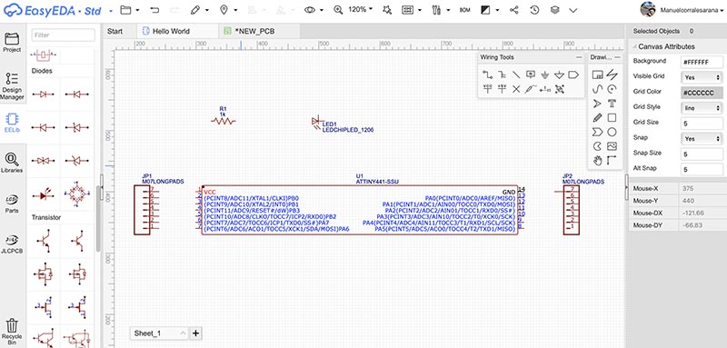
Using EasyEDA i pickup the following electronics:
__ELECTRONICS USED IN THE CIRCUIT__
| ITEM | ITEM | ITEM |
|---|---|---|
| ATTiny441-SSU | ECS-CR2-20.00 B-TR | AVRISPC_SMD |
| RESISTOR 1206 10K | BRESISTOR 1206 1K | VCC |
| 1 Beefy 3 FTD | GND | PT15-21C LIGHT SENSOR |
| LED 1206 |
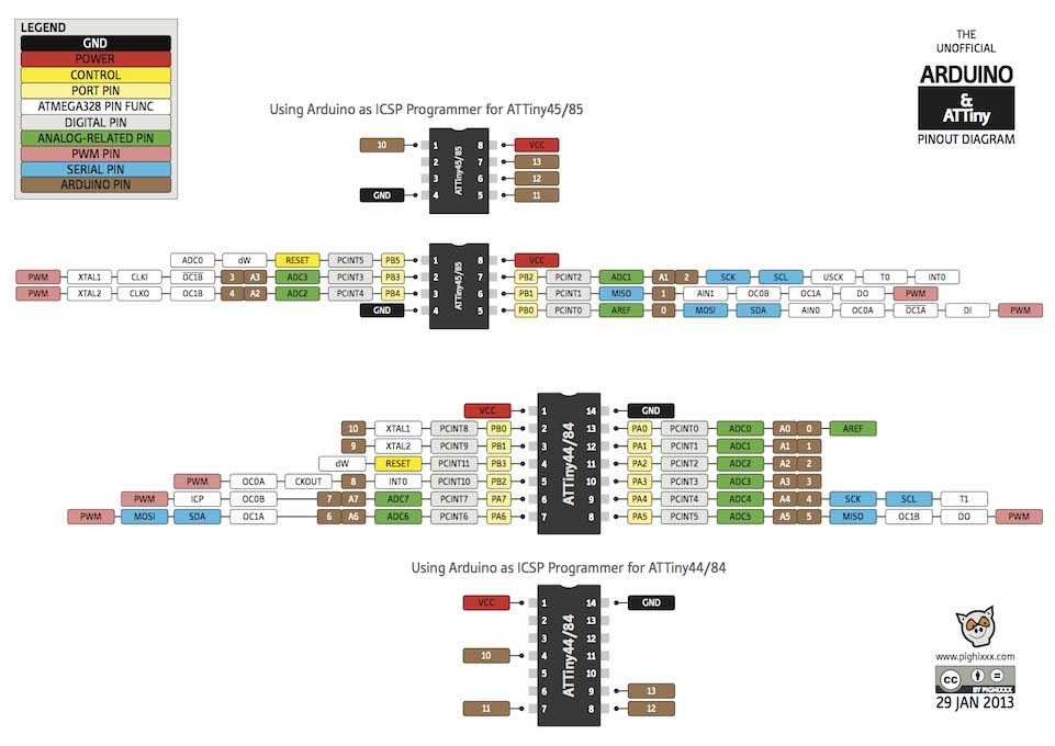
First we have to understand how are the different components arranged in the Microcontroller ATTiny44
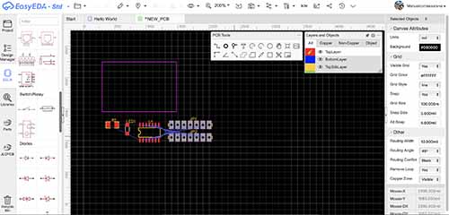
2 Convert the schematic into PCB.
3 Export the PCB into a file with svg extension.
4 I processed it into Fab modules in order to send the information to mill it.
Excersice 1:
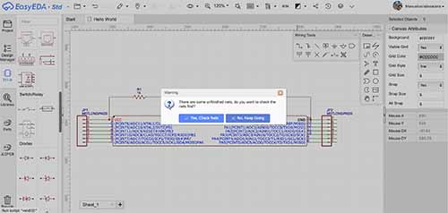
Finally, when i try to program the circuit it doesn’t work because the pinout doesn’t match with the correct one shown in the indication. Probably i download a mistaken one or a component done with error. to solve this, FabLab UCAL create its own components in the library with the work “UCAL”. By this way i assure that the new components are correct. Then i redo all again.
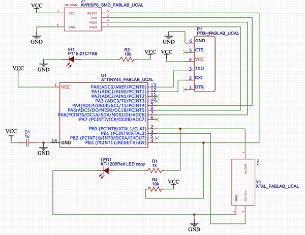
Exercise 2: DESIGN OF THE PCB FOR MY PROJECT
Finally i worked all about this assignment in my project due to the pandemic, because the government closed all educations institutions. I worked in the Makerspace in my school. Here what i worked as part of my Project.
DESIGNING THE ELECTRONICS
I print the schematics to check it that everything is ok, then i go with the PCB.
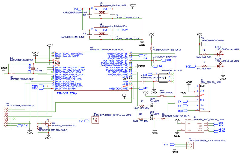
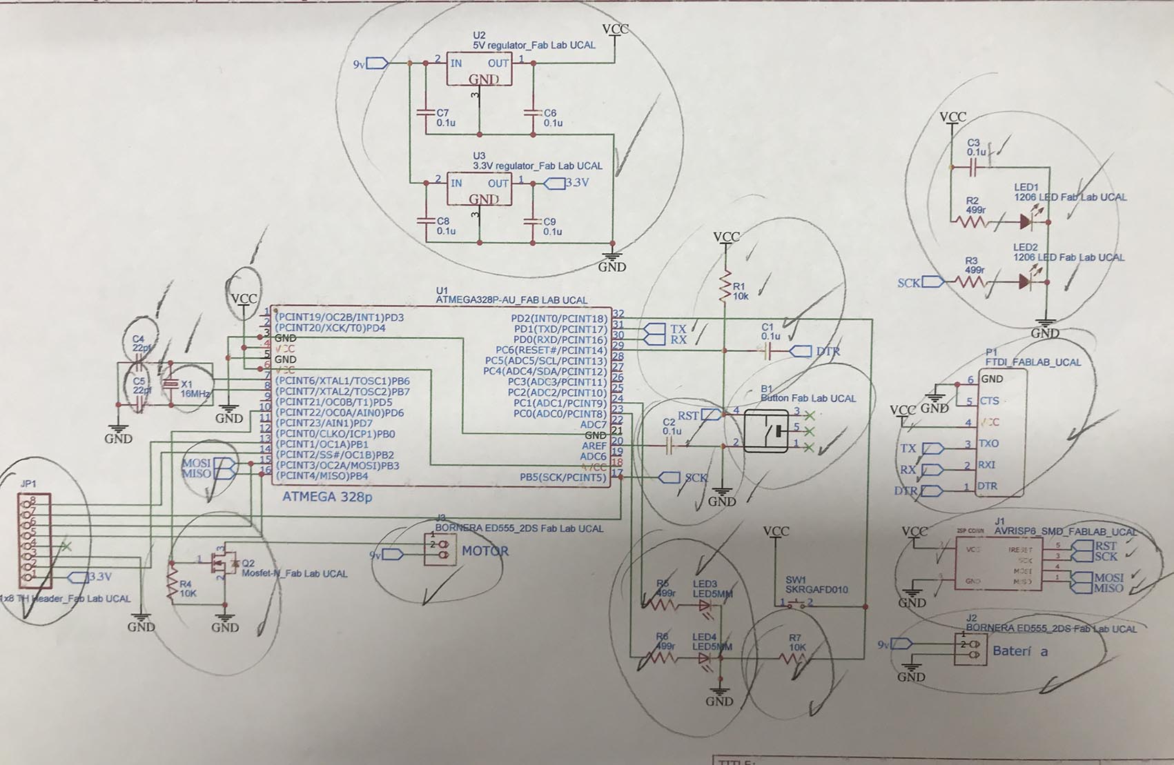 Schematics done in Easyeda online free software
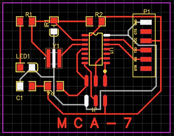
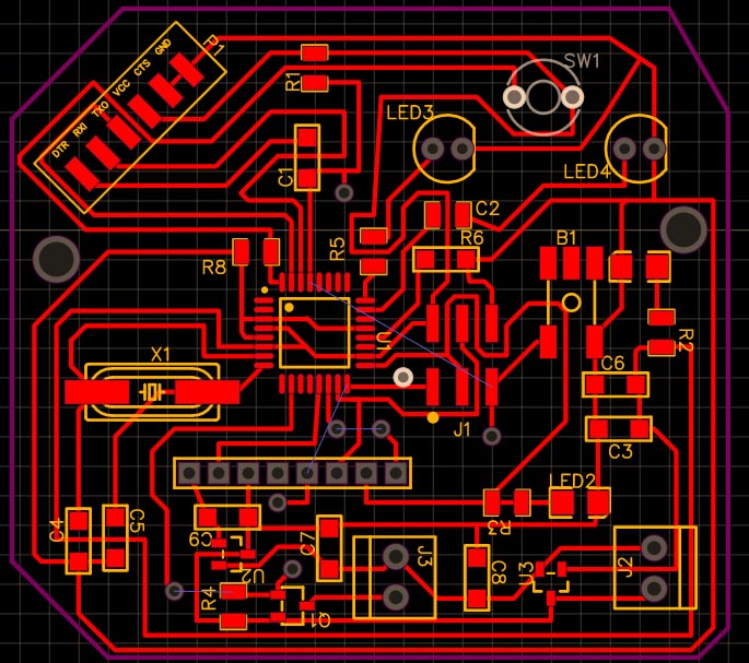
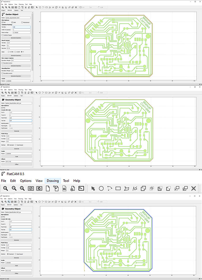
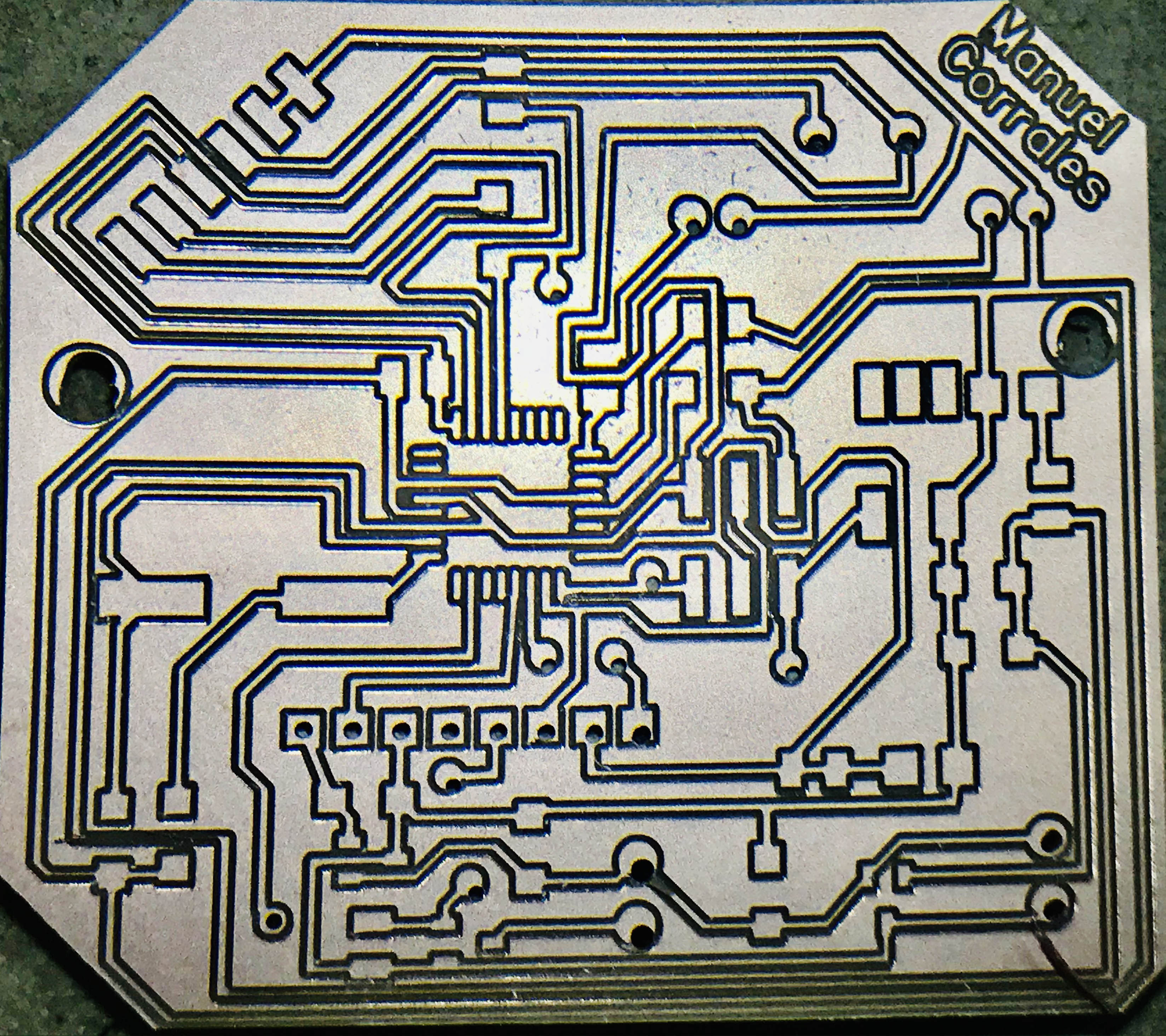
PCB done in Easyeda
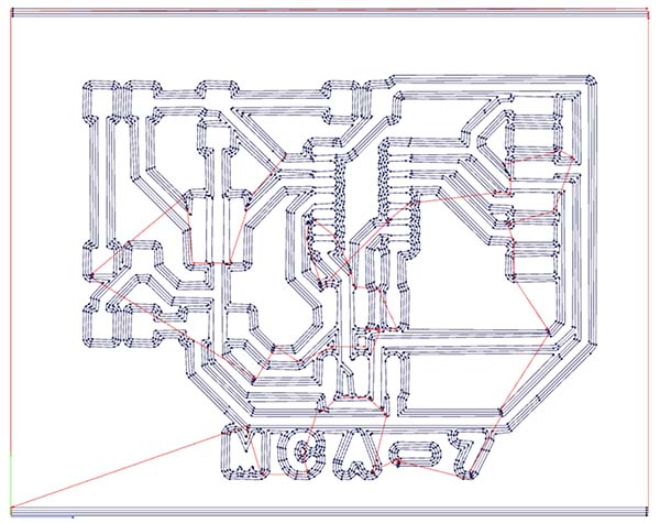
The Gerber view
The Gerber format is an open 2D binary vector image file format. It is the standard file used by printed circuit board or PCB industry software to describe the printed circuit board layers: copper layers, solder mask, legend

I make some corrections to the PCB because some traces were to close and i have to condiser that the RFID has to be a little far away from the LEDs connections. I draw the lines that measures the position of the LEDs and that of the holes.
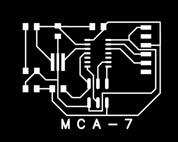
Now the processing of my PCB done in EasyEda by Flatcam First Open Flatcam and in the options section, i select the units in mm. Then i open the Gerber file that contains the information about the Traces. Open Gerber We have to add the configuration of the Milling machine as follows for the traces. Endmill of 1/64
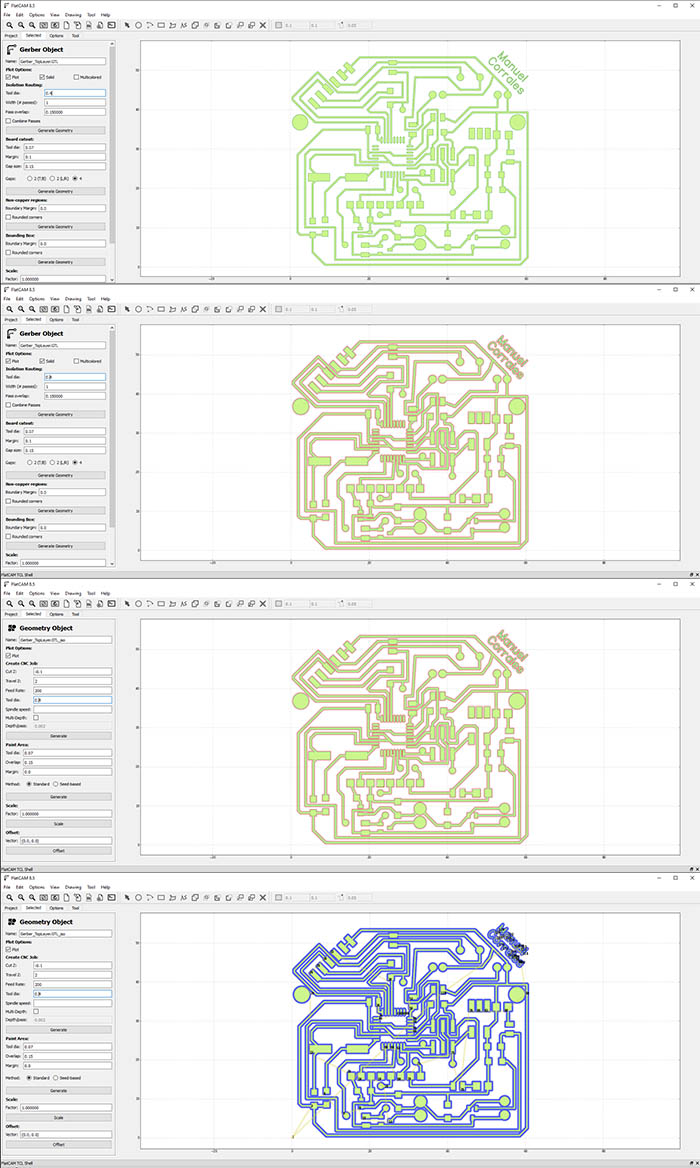
on of the traces, i continue with that of the holes. Endmil of 1/32
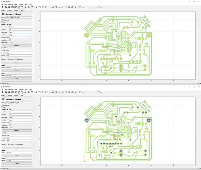
Finally the configuraion of the border. Same endmill as holes.
After having all the archives for drilling the PCB i use the Milling machine to make my PCB
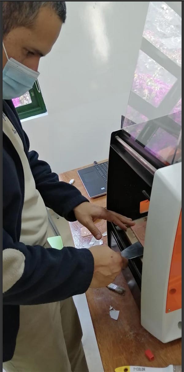
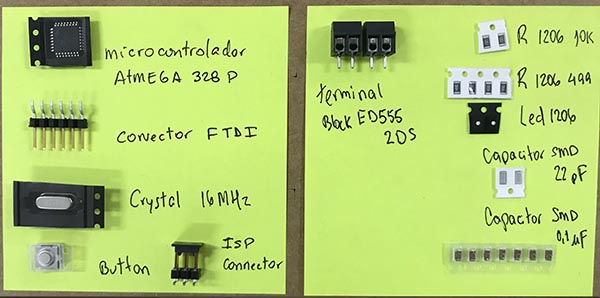
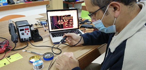
I started the next step: Soldering all the micro components. First place all the electronics in my table, the soldering station, and safety equipment.
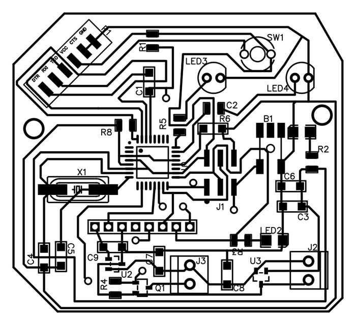
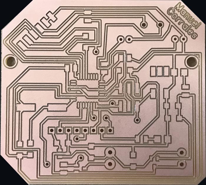
This is the new PCB done where i improve some conections didn´t done.
Then i start soldering all the components.

The Final Circuit Board
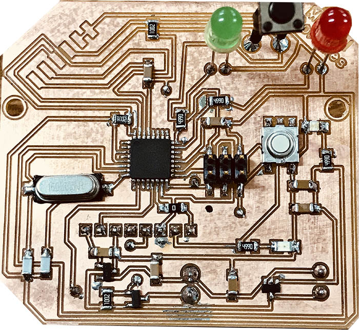
And the total components that are going to be part of the animal robot.
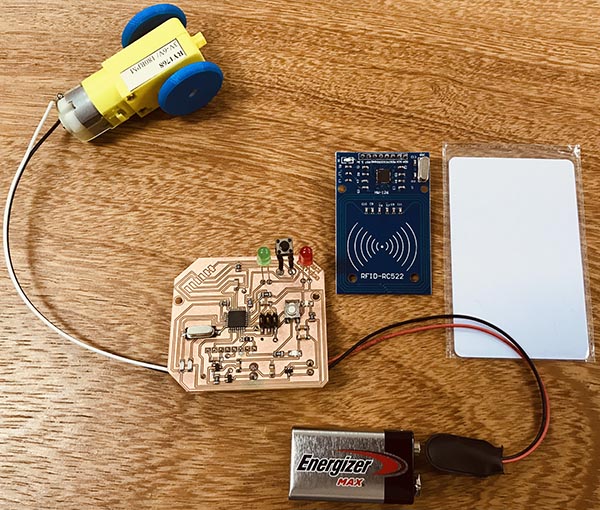
TESTING THE RFID CARD WITH ITS READER IN ARDUINO The RFID reader is attahed to the Arduino UNO and when the White RFID Card is attached to the reader, the blue led turns on.
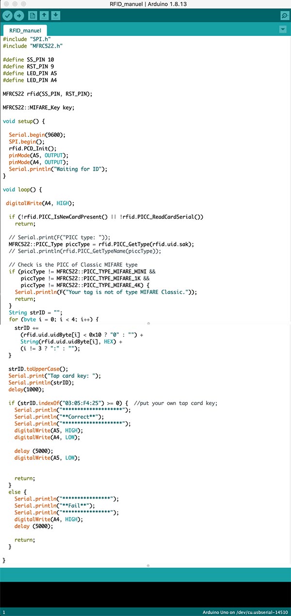
Testing the Arduino with RFID Reader and Card from Manuel Corrales Arana on Vimeo.
Problems found: I found some issues when i make a mistaken conection in the sehcmatic and when soldering the PCB, testing the continuity of one of my components it shows a continuity where there shouldn’t. I solve it by correcting it in the schematics and updating the PCB, milling another board and sodlering everything again. A lot of time but i learned more about electronics and to be careful by checking the shcematics and PCB.