14. Networking and communications
During the lock-down, to keep active for this assignment week, as I had access to a pair of UNO boards, using the pinout diagram of the Atmega 328 I have been able modify the bus serial code in order to used it in this commercial boards. This short help document was provided by Saint Judes’s instructor as support material.
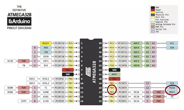
 Using the Pin Out Diagram get sure to define the ports Rx and Tx based using the port pin identification, also the which one where the led is connected
This week’s assignment was to design, build, and connect wired or wireless nodes with network or bus addresses. So I started by building the files of the serial bus example, in the first attempt I downloaded it, converted using an image to Gerber software, and tried to scale it using the flatcam software. That gave me boards with the wrong dimensions for the footprints but also difficult to solder and connect, so this was the first failed attempt.
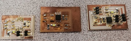
Then I used the Monofab workflow using Fabmodules to prepare the pcbs for the bridge and a pair of nodes.
Those boards were solder and testing to proceed to burn the bootloader and charging it the examples, was experiencing some trouble with the tracks which were fixed using hot silicone to attach the pins to the board.
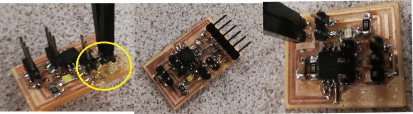
I start uploading the code example to the boards following this documentation prepared at St Jude’s Fab lab to support this assignment aiming. everything was going well until I test it using the serial monitor, apparently, a shortcircuit that was tried to debug, next step will be to redesign it and test it using the code example and the nodes boards already built .
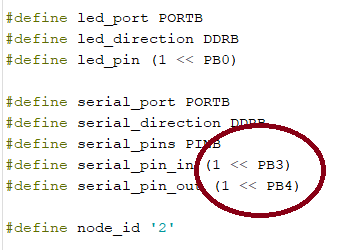
Then I started to fulfill the task of redesigning the bridge board, I Followed the serial bus example to prepare my own version in Kicad.
Because in previous versions of this board I experienced problems with the stability of tracks of pin connectors components to the heating of the soldering iron, I modified it changing the Dimensions of the footprints in the option properties which appear once right-clicked above the footprint.

It was until I completed the whole process of soldering it and bootloader burning, after uploading the code to the board that a terrible fail was identified, I forgot to include more than two connections to Tx, Rx, and VCC FTDI pins in the Schematic, I tried to rescue it using wires but it didn’t work.

I fixed the mistakes in KICAD and prepared the fabrication files, soldered the components in a new board, and tested it burning the bootloader and uploading it the code for the bridge (just be sure to change the number of the node to zero), then it is connected with the FTDI cable to open the serial monitor and sent it a #, if it is working the led should light 2 times when the number of the node is written and is sent it pressing enter.
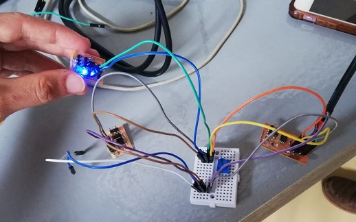
The next step is to test the communication connecting the RX and TX pins of the board to the other two (already built boards) between them, the same code needs to be uploaded to each board (just be sure to change the number of the node to 1,2,3,....n,
I had this false positive essay, because every time I pressed enter key the led lighted but it was not working because it return just that action insted of t wo ties blinking, also when it was connected using the FTDI cable to could see the board’s answer to that action in the serial monitor it shows wrong messages.
This problem was because the bootloader was burned indicating that the board counts with a 1Mhz internal clk, it was changed to 8 Mhz and then the boards worked, as the node boards were a little bit damaged because the weak strength of the tracks, one the nodes did’nt work because it had shortcircuit.
Files