5. Electronics production
Fabricating PCBs
This week’s group assignment was to characterize the design rules for the PCB production process. One of the machines we have access to is the Roland monofab SRM20, here are specs and Technical support to get more resources about th machine.
The process to design a PCB using this machine is the following.
-
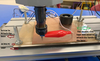
Be sure that there is a sacrifice board with heigh enough and leveled to attach the PCB sheet that we are going to mill.
-
Attach the PCB sheet to the surface with double side tape cover all the surface with just one layer to avoid as much as possible miss leveling.
-
Connect the USB to the machine and Open the software Vpanel, use the controls to set XY and Z origins.
-
To be precise in the setting of the Z-axis, adjust the height of the milling tool with the tool provided to press and free the screw of the collet.
-
Use the X10 and X1 steps to adjust cautiously the zero position to avoid breaking the tool.
-
Then process the files on Mods or any other software which brings you the option to export NC or RML code.
-
Send it to the machine using VPANEL software.
-
I learn from this documentation that good practice is to set the Zaxis with the help of a multimeter set on continuity mode.

To characterize the machine I used Mods to set the cutting file of the line test.
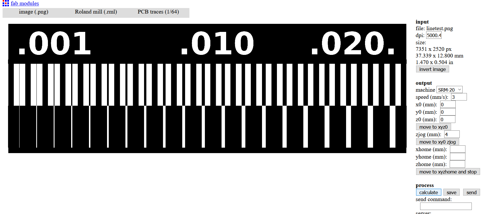
- Input format (Image PNG)
- output format (Rolland mill)
- Process (I test PCB traces 1/64 and 0,010)
- Adjust speed to 3 or 4 mm/s
- zjog is the travel of the tool along z-axis between movements, so I used 4mm
- Then calculate the work and save it
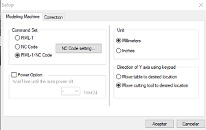
Be sure that RML-1/NC-code and millimeters options are selected in the emergent window of the setup button. Click on the cut button, then add the file in the list and select output. The machine should start work.

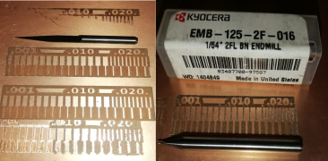
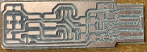
Here are the results after solving some miss leveling which generated some failed essays.
5. Electronics production
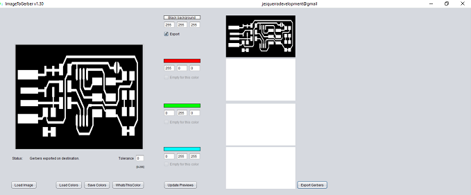
Gerberfiles - imagetogerber software was used to set the image and stablish a black background.
G- code files
- open the Gerber file on Flatcam
-The first step is to set the units for the project, in our case is mm, after, configure the tool diameter to 0,3 mm for the isolation route, then generate geometry object.
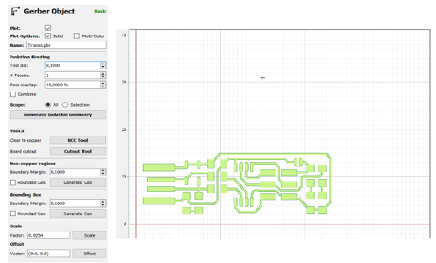
Once the geometry object is created, you can inspect that the route goes parallel to all the pcb routes, effectively isolating them. Then, other variables must be set to create the cnc instructions files:
Cut Z: -0,15 (depth of carving).
Travel Z: 2 (height of the tool when not cutting).
Feedrate: 15 (speed of the tool while cutting in mm/minute).
Tool diameter: 0,3 or 0,4 (the same as in the previous step).
When the button generate is clicked, it creates the g-code for the isolation route of the pcb. It must be saved with .nc extension.


Following the same steps, the g-code for cutout can be created. For the board cutout, more depth is required, as well as another tool apropriate for cutting.
Preparing the milling
The milling machine must be prepared with the right tool. The board must be tightly attached to the base using double stick tape and screws.
it’s recommended to set multiple zeros. Current continuity can be used for zero setting, so, a cable is soldered to the board and another cable is connected to the tool, so when there is continuity, a zero is set.

Sending the G code For the execution of the g-code in this machine, the file is opened with bCNC.
bCNC has the autolevel option, and several zeros are set for Z axis.
The g-code file is opened in bCNC, and, before starting the job, a visual check of the machine is performed, the pcb must be aligned and firmly fixed, there must be no objects between the tool and the board.

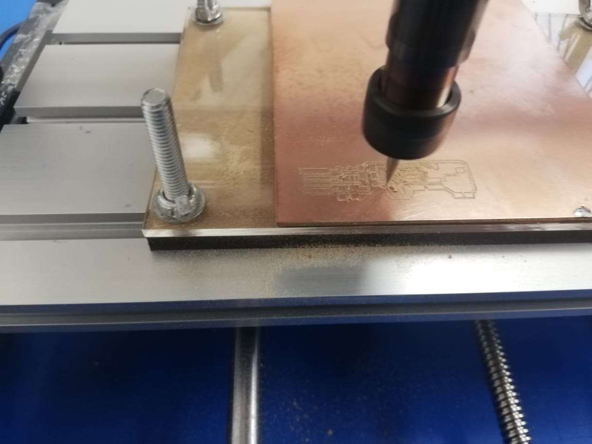
When the isolation route is done, the tool is changed, either to cut the board or to mill non copper areas. Whenever there is a change of tool, it’s good practice to reset the Z axis’ zeros.
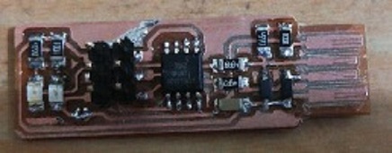
Soldering Components
Its important to improve soldering skills in order to obtain better outcomes. (At this assignment, I had a pair of failed essays, before to build a workable circuit)

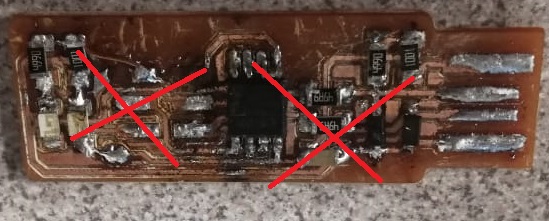
At the end Its useful to put a double side tape square under the contact for usb connector.
Programmming the ISP
I consulted this doccumentattion to guide me o this part of the work
The following steps are commands entered on the ubuntu terminal. First, download and install the drivers and libraries for the AVRISP on the computer:
apt-get install flex byacc bison gcc libusb-dev avrdude

sudo apt-get install gcc-avr

sudo apt-get install avr-libc

sudo apt-get install libc6-dev
Download the Firmware
Go to the folder where you want to download the firmware. Use “cd [folder]” command to go there.
wget http://academy.cba.mit.edu/classes/embedded_programming/firmware.zip
Unzip the firmware
Unzip firmware.zip
Go to the unziped folder. Use “cd [folder]” command to go there.
Program the ISP Check if the AVRISP is conected to the computer and to the programmer, and also that the programmer usb port is connected to the pc (for power).
Continue on the terminal, press enter after each command. Read the output of each command to make sure it executed usccesfully:
make clean

make hex

make fuse

make program
If everything went well, list the usb devices and look for the USBtiny, that means the ISP was programmed correctly and the computer recognizes it.
lsusb


Testing the ISP
The board is now a programmer for other microcontrollers, but it have not been tested by programming another board yet.