7. Electronics design
During this week we worked at St. Jude on the Group Assignment
Individual Assignment
This week’s assignment was to redraw an echo hello-world board, and add at least a button and LED, also we had to apply proper design rules, make the board and test it.
So, for this task, we received an explanation about the basics of designing and making this kind of devices. Based on electronics production week programer and the echo hello-world board, I learned that the common “formula” to design around this kind of micro-controllers in PCBs always include a 1 uF capacitor between GND and VCC (for voltage decoupling) and a 10 k resistance between Reset and VCC (to avoid uncontrolled resets of the microcontroller).
After that, it is possible to continue connecting other sensors or actuators to the rest of the pins which may also need other passive electronic components such as resistors, capacitors, or transistors to work correctly.
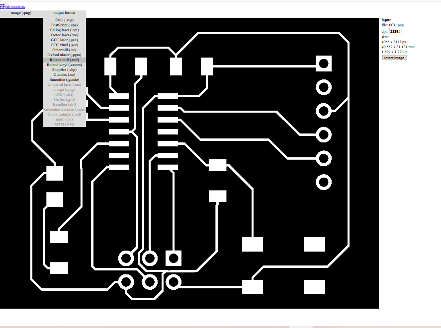
We started using Kicad software this week: In the starting window there are different options to manage files and the editors which are used to create schematics, symbol editor, edit the PCB layout, footprints, a Gerber Viewer, and other features useful to edit graphics and text in the files.

You can find most of the standard symbols and footprints for common components, but there is a custom fab library which contains symbols and footprints and can be downloaded here.
Once the library has been downloaded, go to the preferences tab and select the “Manage Symbol Libraries” option, select the “Fab” one in the global libraries list, this is going to be needed to assign the footprints to each symbol included (this has to be done only the first time working with the software).

The drawing of a board starts with the schematics. Select the “Schematic Layout Editor”, there you can add the symbols for each component. For this example, we added an Attiny44, capacitors, resistors, a 20Mhz resonator, an LED, a button switch, and finally, FTDI and AVRISP connection pins. Once that all the components are included to the schematic, we started making all corresponding connections between all of them.
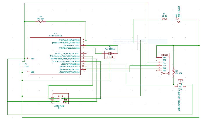
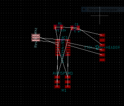
When the schematic is finished, assign the footprints (1) to each symbol of the schematic and generate the netlist (2). After that go to the PCB editor (3) and press the option “Update PCB from schematic”, after doing that, if everything went well, the software is going to show the relations between footprints with white lines that work as a guide to draw the routes.
A very important aspect for PCB fabrication is the design rules. They must account for the physical size of the components, milling machine capabilities and tools dimensions. In Kicad, go to Design rules and click on net clases, there you can define different parameters for each net class. A simple board like the one for this week can have only one net class. And according to our tools and the milling machine resolution we set the net width to 0,4 mm. The microcontroller pins width is also 0,4 in average. The clearance was set to 0,2 mm (half of net width).
Once all the connections are ready, you can switch to the Edge-cuts layer (to the right of the screen), and draw the Border of the PCB. This will be the external line of the PCB to cut with the milling machine.


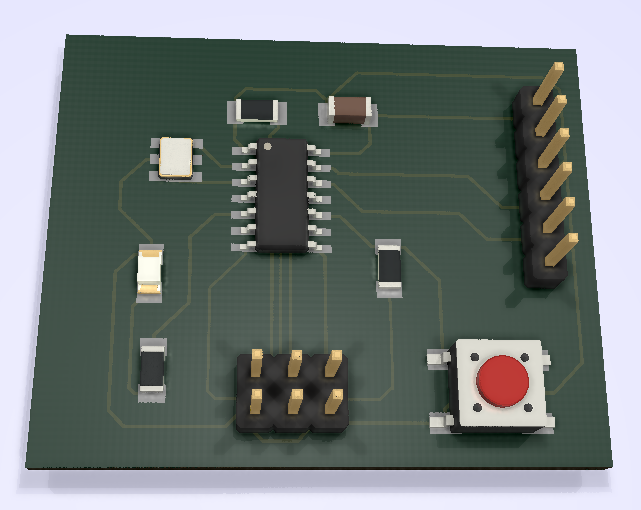
Another useful option that this software offers and could help the design process for Digital Fabrication projects is the 3D visualization of the results.
To export the work, there is a button in one of the upper toolbars with a plotter icon, in the emerging window all the settings can be defined, this depends on the workflow for the machines that we have access to in the lab. But before exporting, it is necessary to set the auxiliary axis origin. This will be the origin for the machining jobs.
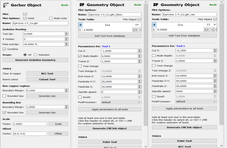
I first exported Gerber files that were to be processed in Flatcam to generate a .nc file based on the design rules for the CNC milling machine available at Fab Lab St. Jude.
As I didn’t know the workflow for other kind of machines (such as the Monofab SRM 20), I tried exporting to SVG files, used Inkscape to save a .png file, and then configured that on Fab Modules. The .svg files must be modified a little bit, grouping all the objects, adjusting the page size to the content on the editing tab. It is also very important to modify the resolution of the image to a higher value to ensure the image accuracy order to be well interpreted by the Fab Modules.

As seen on the electronics production week assignment documentation, you must import the .png file in Fab Modules, click the insert image button, in the output format select Roland mill (.rml), then select the process based on the tool that you will use, check the values and click calculate, save it, and that file can now be used to send it to the machine using the cut button on V Panel software.
I tried that workflow for traces and drilling points but I had some trouble positioning the holes in the exact place.
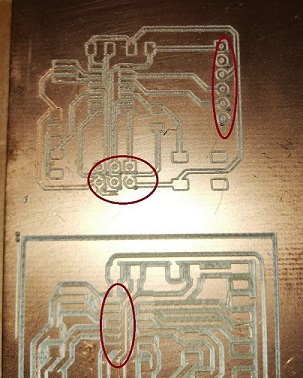
Then I went back to the workflow with FlatCAM software to try again. I noted that the errors I was having with the files in the monofab were related to not establishing the auxiliary origin point in Kicad before exporting to gerber files.
To work with FlatCAM .nc files, it’s just necessary to set the V panel software to NC files mode, this mode works with a different coordinate system called G54 but I have not researched much about what it means.
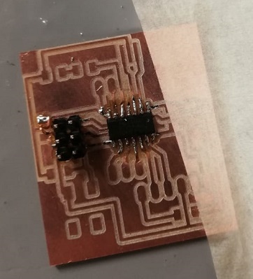
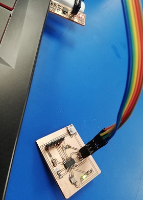
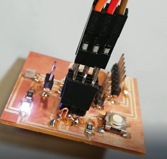
So I remade the board for this assignment and used it to test the isp programmer fabricated for the electronics production assignment.
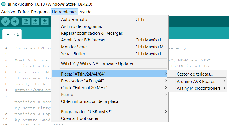
In order to program these boards based on Attiny microcontrollers using Arduino IDE go to Files –> Preferences and paste the following in the manage external board URLs:
https://raw.githubusercontent.com/damellis/attiny/ide-1.6.x-boards-manager/package_damellis_attiny_index.json
Then go to the Tools tab, click in managing libraries option, write Attiny in the search bar and click the install button.
After that, go back to the Tools tab and set the options as follows:
- board > “Attiny/24/44/84”
- processor > “Attiny 44”
- clock > External 20 MHz
- programmer > UsbtinyISP
- burn Bootloader
now your board is ready to upload code to it.
Just to test it works, I uploaded a blink example code available in Arduino IDE
Files