10. INPUT DEVICES
This week I worked on
Individual assignment:
- Measure something: add a sensor to a microcontroller board that you have designed and read it.
Group assignment:
- Probe an input device’s analog levels and digital signals.
I have continued using my weekly planning in which I have updated my activity in FabAcademy
10.A. INDIVIDUAL ASSIGNMENT
This week we are still in confinement for the coronavirus pandemic. The FABLAB continues closed.
In this assignment I am going to design a board, for this I have based on the one I already designed in the assignment of week 7, “Electronics Design” the board Echo Hello Board. From there I have included new components to be able to measure temperature using an infrared sensor that is the one that I will use in my final project.
10.A.1. Infrared sensor
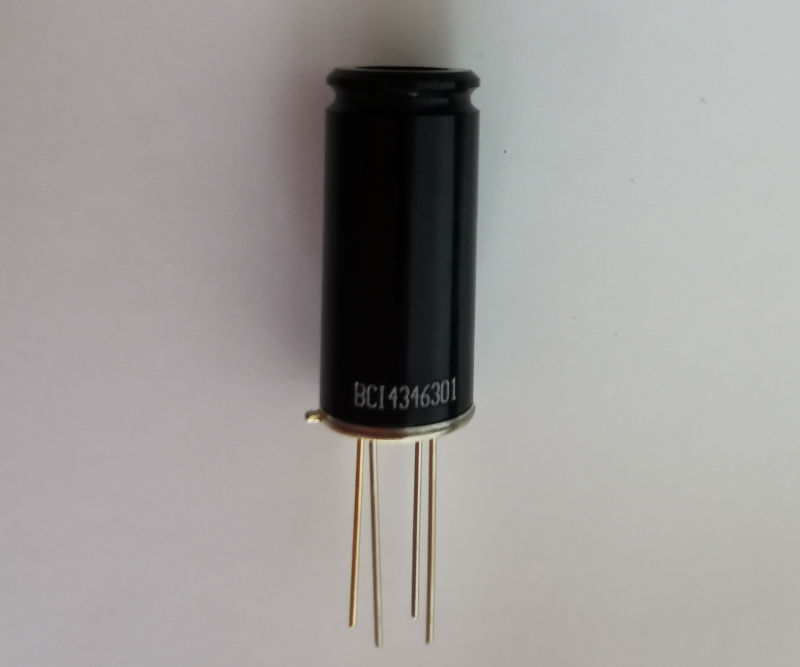
First I have identified which sensor I want to use like a input of my circuits board.
My infrared sensor is: MLX90614 BCI 4346301, in this link I have found the Datasheet information for this sensor.
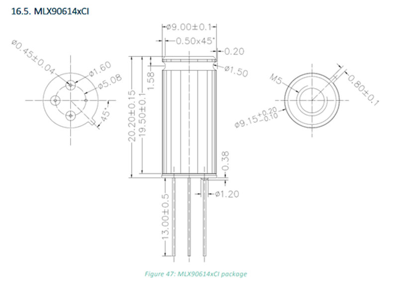
10.A.2. Infrared Sensor Features
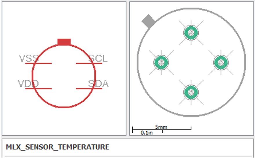
This is the geometry and measurements of my sensor:
10.A.2.1. Pin definition of the nfrared sensor
In the datasheet of this sensor I study its description and its pin definition.
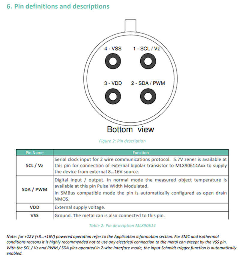
In this way I already know how to connect the four pins that this sensor has.
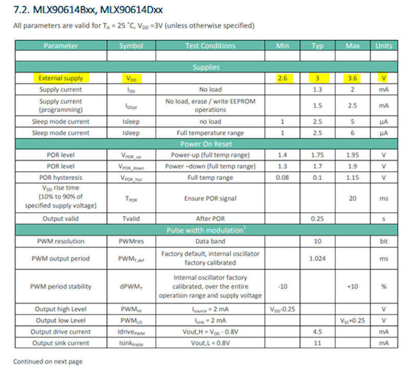
10.A.2.2. Electrical especifications of the infrared sensor
I also study in the datasheet other data that I will need.
For the BCI family of sensors, these are the electrical specifications:
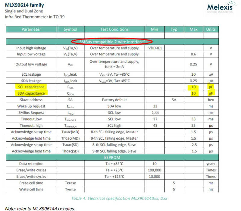
10.A.2.3. Comunication protocol of the infrared sensor
As for the communication protocol, this type of sensor communicates through I2C and all the sensors that I will need to connect to develop my final project can be connected to the same communication BUS.
10.A.2.4. FOV of the infrared sensor
Since my sensor is BCI type, this is the diagram where I can see the sensor’s field of view.
FOV = Field Of View
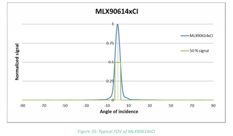
This model of sensor has a very narrow field of view FOV, which is what I am looking for, because I am interested in the fact that the temperature measurement made by the sensor is accurate, since it will only measure the area to be crossed by the human limb (hand for example) .
The measurement will not be affected by surrounding objects, it will only measure what we want it to measure.
The green area represents the effective measurement area.
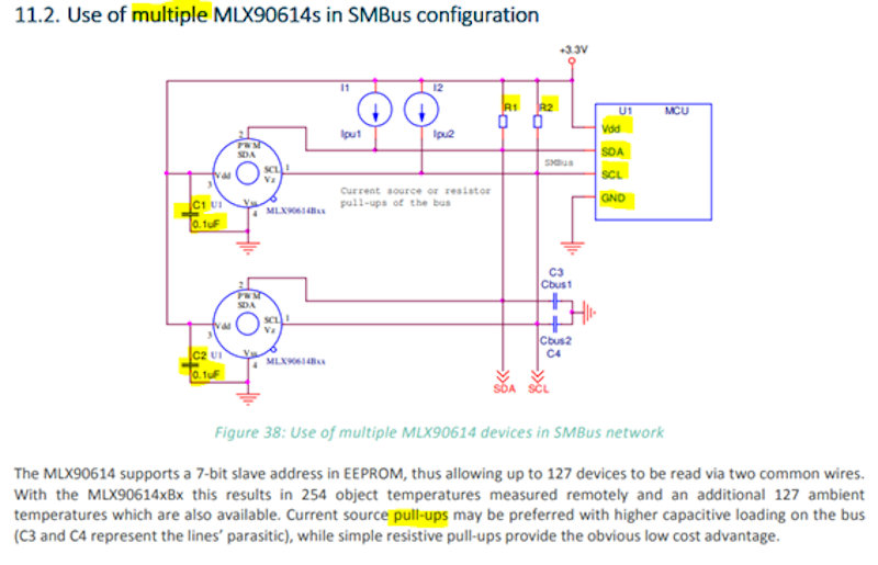
10.A.2.5. Use of multiple infrared sensor
In the datasheet I also find data on how to connect my sensor in a multiple way, which is how I need them to be connected in my final project, in which I will need a number that I do not yet know of sensors connected in series.
These are the elements that I will need on my board:
On a board I will have the sensor with the capacitor.
On another board I will have the microcontroller (I am going to test with the ATtiny 44) and the two Pull-ups resistors.
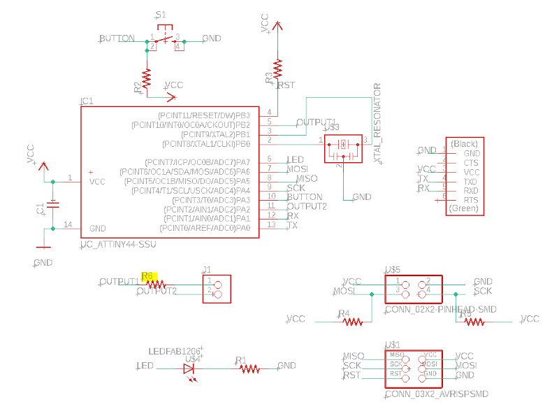
10.A.3. Microcontroller and components of Input device
To make this board to serve as an Input device, I have based on the one I made in the assignment for week 7, the “Echo Hello Board”, since I will need those components, plus the connections for the sensor I want to introduce and the necessary components that must accompany the sensor.
The Microcontroller that I used in the design of that board is the ATtiny44 and it is the one that I am going to use now too, so I will study the ATtiny44 Datasheet to know its pin configuration and its characteristics, before making my new board design based on this microcontroller.
10.A.3.1. ATtiny44 Microcontroller Pin Configuration
The pinout of this microcontroller is this:
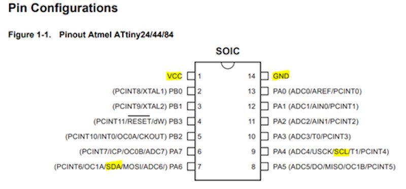
I will have to connect the pins of my sensor to these pins of the microcontroller.
10.A.3.2. Board design using Eagle
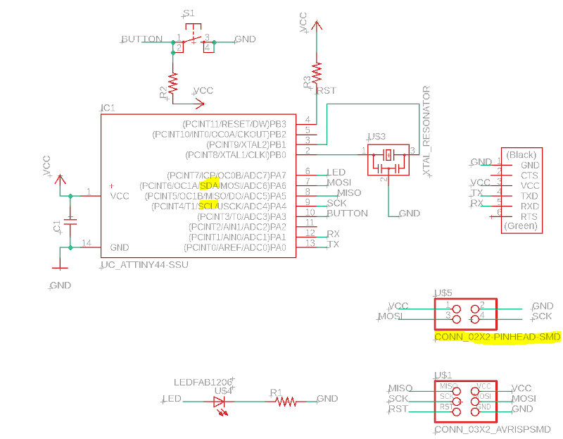
As I am going to build on the Hello Board that I already did, I start from the Eagle project that I did in week 7, I copy it as another different project from week 10.
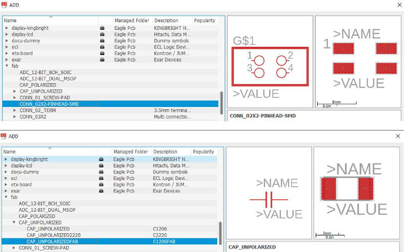
Now I need this other 2x2 connector that has VCC, GND, SDA, SCL connections.
I include it in my scheme.
With this connector we can communicate through I2C, to which we will connect and serialize our sensor chain. I will use multiple infrared sensor.
The two pull-up resistors must also be connected, to do this I connect them to the connector.
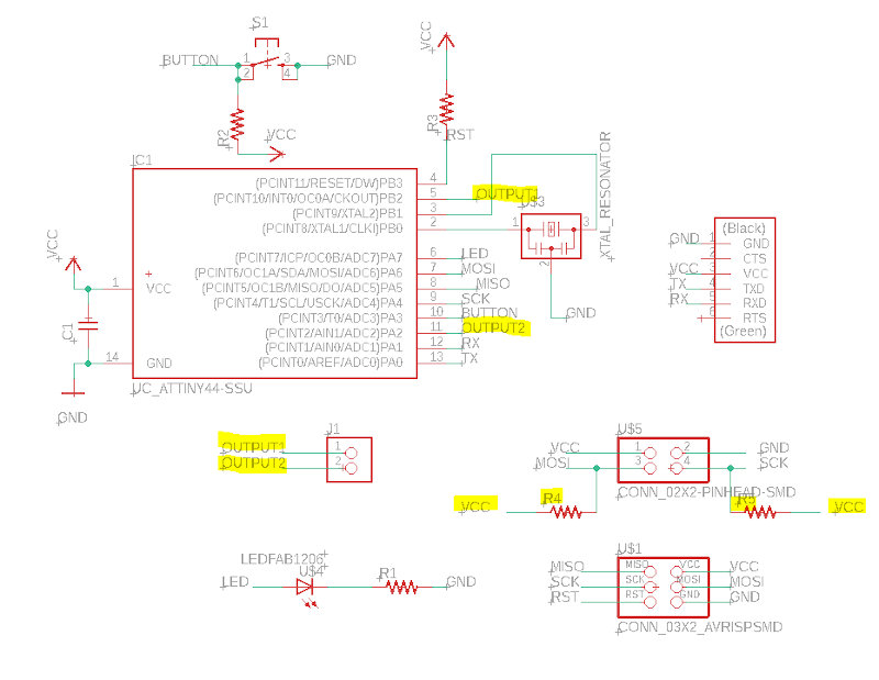
I also leave my board ready to put the OUTPUTs when the time comes, and use the free microcontroller pins.
I remember saving, and now I go into Eagle to the interface to configure my board leaving the schematic mode.
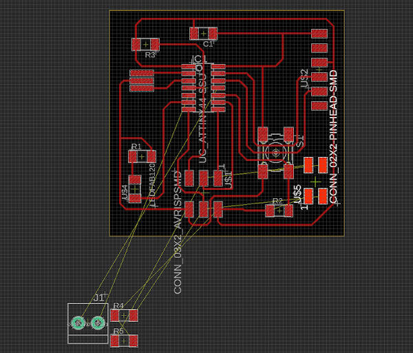
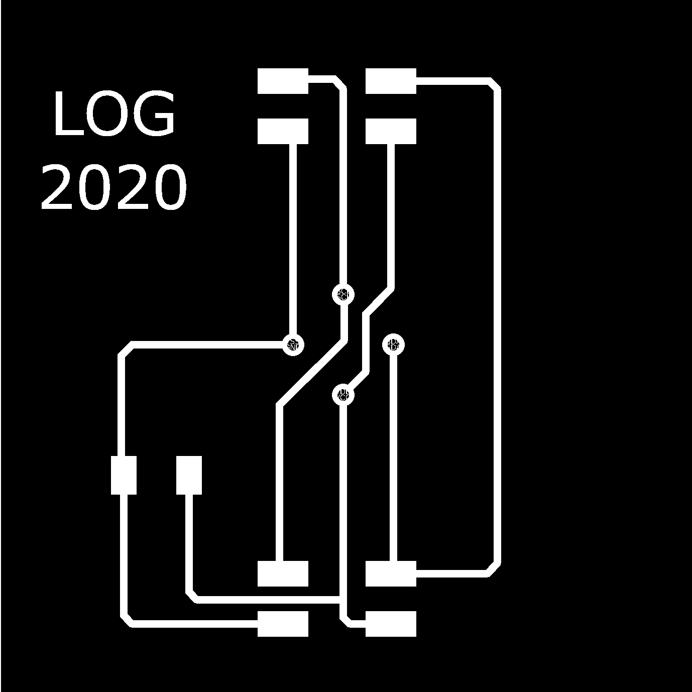
I have to organize my connections to have a board that can mill and weld its components.
After struggling a lot with the connections, I had to introduce a resistor (R6) to be able to bypass one of the circuits, and the diagram looks like this:
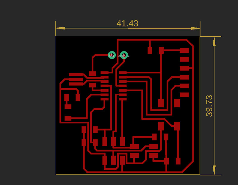
The design of my board, has been like this, (with line width of 16mil) and after doing a DRU with the preconfigured design standards, and a check, everything is correct.
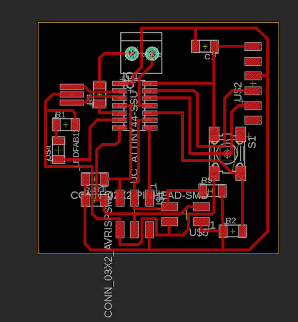
To prepare the plate for milling, I must leave only the layers to be machined visible. And they are (Top, Pads and Vias):
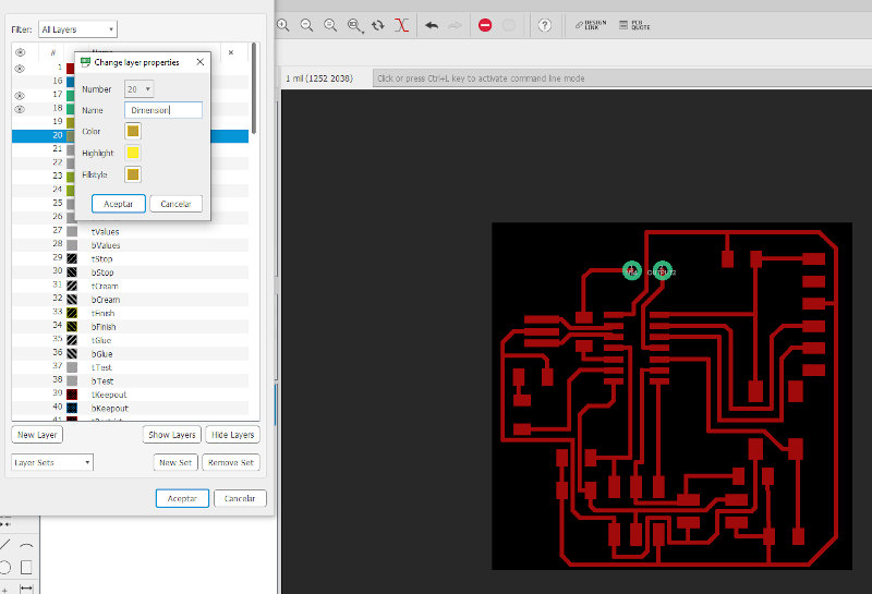
I adjust the dimensions of my board by activating layer 20 Dimension (using the move command).
All ok.
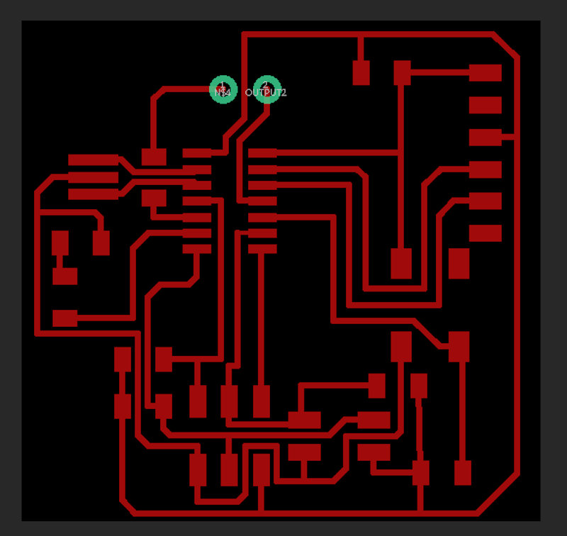
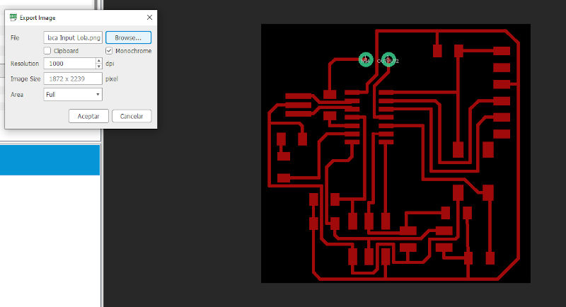
I export the file as a png image, in this week’s assignment folder with the name “Placa Input Lola”.
These are the export parameters.
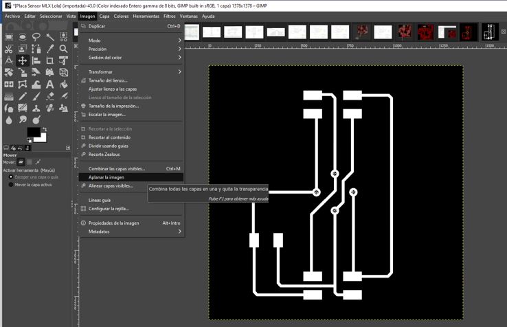
I open my image with Gimp.
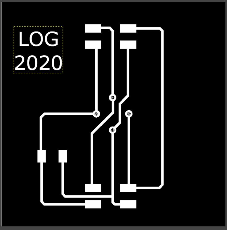
I modify “canvas size”, use “flatten image”, put text: my initials + 2020. I export the image.
It looks like this:
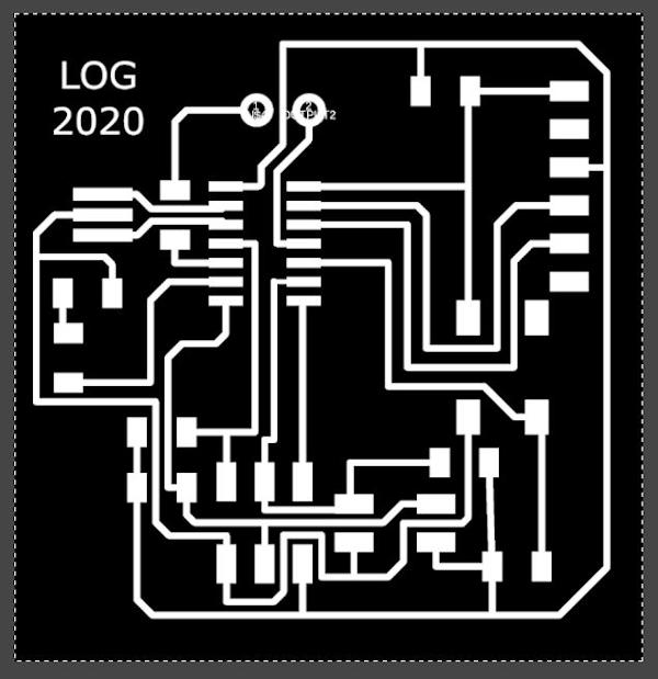
This is the board that I have to mill from my circuit recorder / cutter when I have access to the lab and machines to do it.
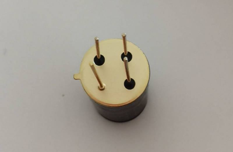
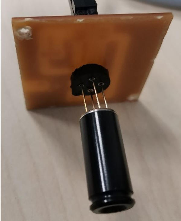
10.A.4. Infrared sensor board
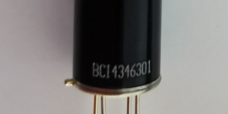
My sensor is this, with these pins:
10.A.4.1. Infrared sensor board design
To connect it to the board, you will need a connector of this type:
To have this component available from Eagle and be able to introduce it on the board that I have to design, I must first create it, since there is no similar one.
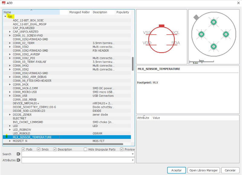
To create this new component: MLX_SENSOR_TEMPERATURE I have followed this tutorial .
After creating it, I have modified the fab library, to which I have added the scheme and symbol of the MLX sensor to insert into the board design.
I copy and paste the file from the new library into Documents \ EAGLE \ libraries and replace the file that is called the same. (fab.lbr)
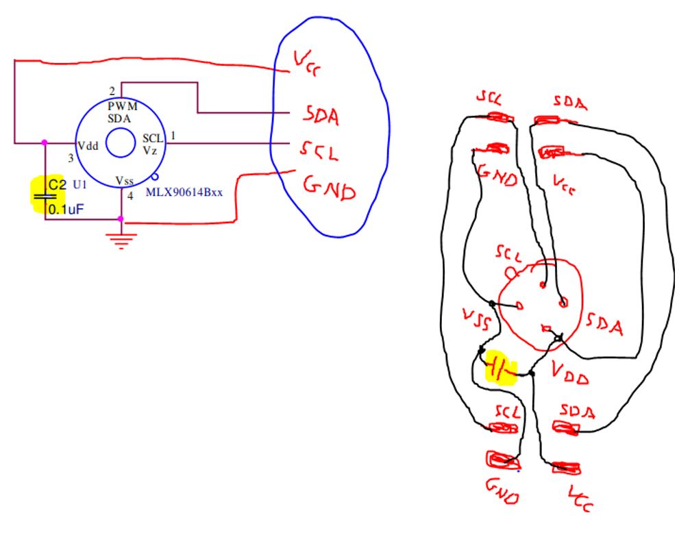
Once I have the new component available from Eagle, I have to do the design of the board for the sensor, this would be the sketch:
From Eagle, I create a new project called “MLX Sensor Board”
I create the scheme, inserting from the new fab library that I have installed (fab.lbr), the sensor that I have created with the pins and characteristics corresponding to the infrared sensor MLX90614 BCI 4346301 that I am going to use as INPUT.
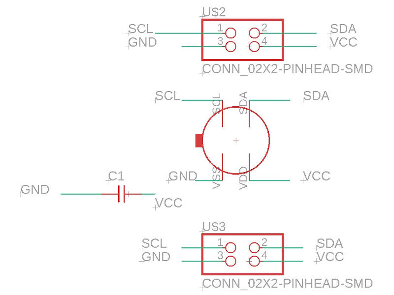
I also insert the rest of the components necessary for the board to work.
These components are two 2x2 connectors and a capacitor.
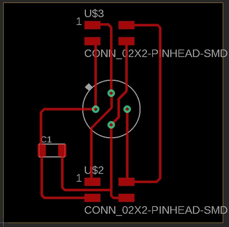
The schematic design of my board is this:
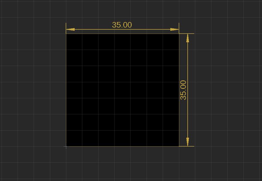
From “Board” mode in Eagle, I configure the board layout. As the size of the board between the yellow lines is very large for the components it has and must fit in the part designed and printed as a test in 3D printing, I measure the space it has to occupy and it is 35mm.
Then I change the units of work in my Eagle file type brd. In Grid, I put “mm”, I put spacing between grid points of 5 units.
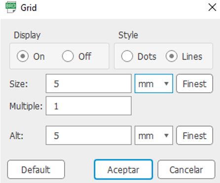
With the Dimension layer active and the move command, I modify the size of my board so that it measures 35mm x 35mm.
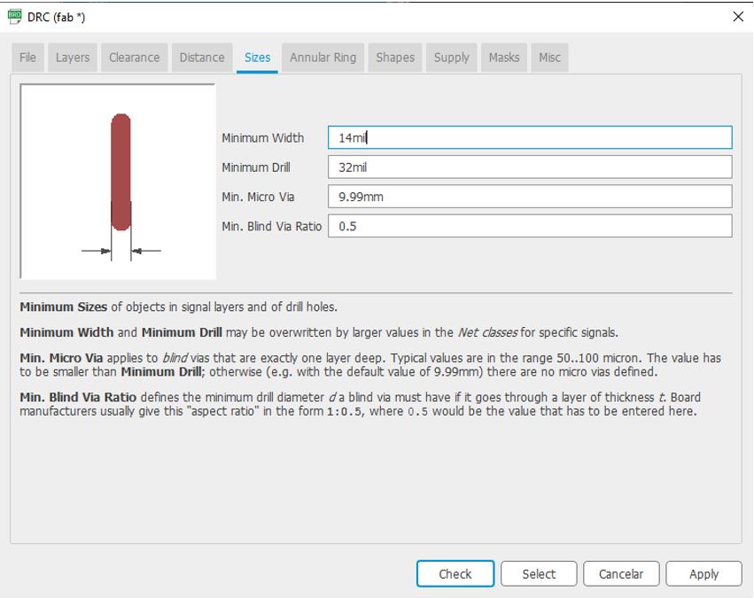
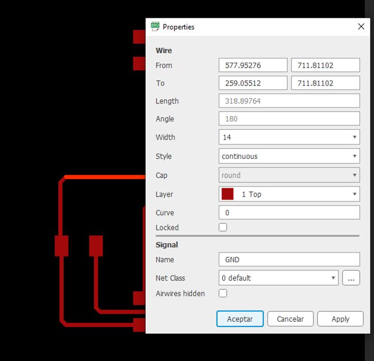
Then I check the thickness of the circuits in the imposed design rules, and put circuit width width = 14mil.
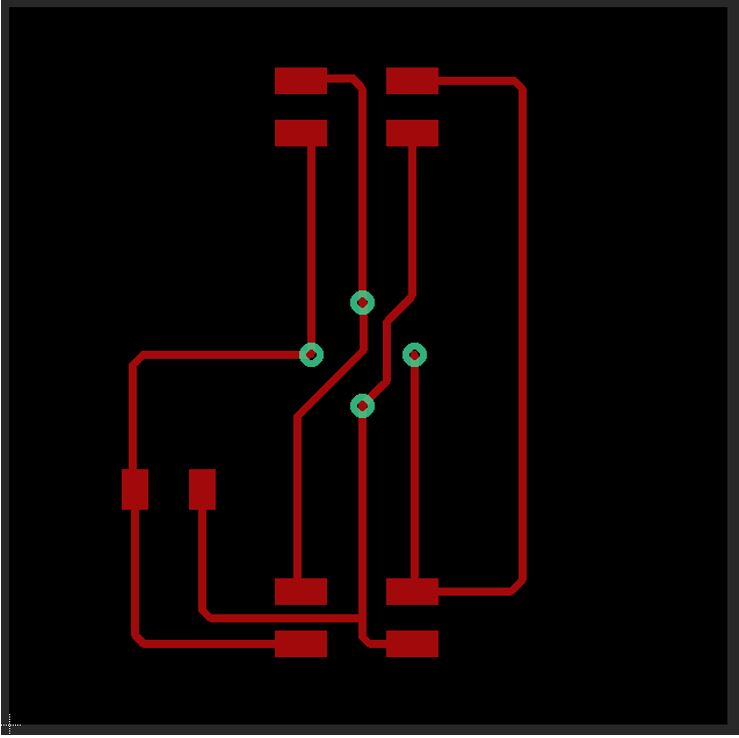
I configure the layout of the board connections and the result is this:
As with the previous board, to prepare it for milling, I must leave only the layers to be machined visible. And they are (Top, Pads and Vias):
I adjust the dimensions of my board by activating layer 20 Dimension (using the move command).
All Ok, since at the beginning I was careful to configure the size of the board, and there have been no changes, neither voluntary nor involuntary. Check done.
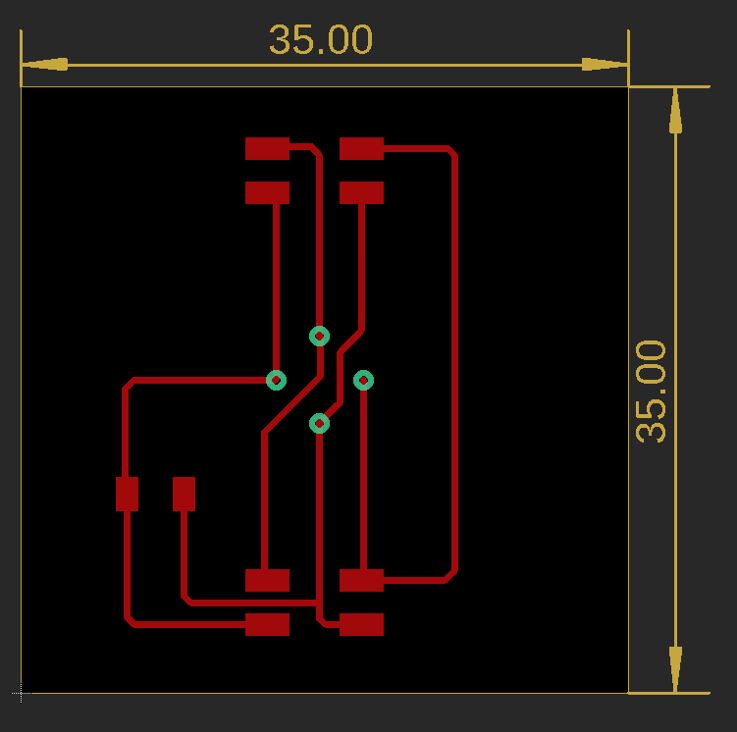
I also check the thickness of the connecting lines.
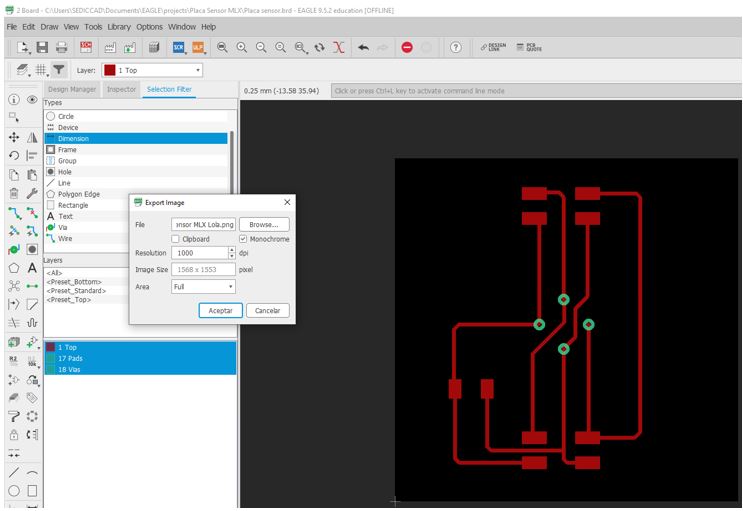
Then, I export the file as a png image, in this week’s assignment folder. With the parameters indicated in the following image:
I open my image with Gimp.
I modify “canvas size”
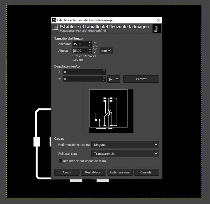
Use “flatten image”
I put text: my initials + 2020.
I export the image and it looks like this:
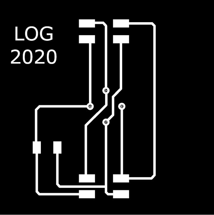
This is the board that I have to mill from my circuit recorder / cutter when I have access to the lab and machines to do it.
10.A.4.2. Infrared sensor board milling
As of May 18, I already have my printed board.
For this, even though we are still in confinement, I have to go to Álvaro’s house, who has brought the circuit milling machine home to be able to work on this assignment and things for the final project. We have taken precautions and respected security measures.
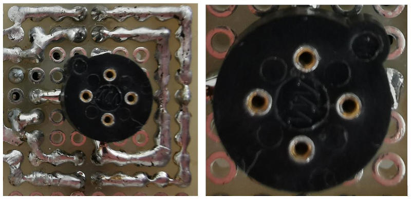
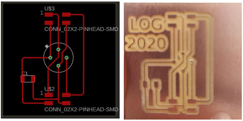
The milled board looks like this:
10.A.4.3. Infrared sensor board welding
Next, the electronic components were tin soldered - 1 Capacitor C1 = 0.1 µF - 2 4-pin I2C connectors - 1 Round 4 Position Transistor Connector, TO-5 Gold Plug Through Hole
After milling the components on the sensor board this is the result:

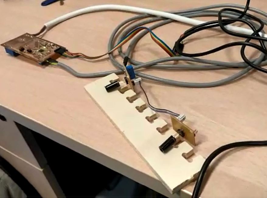
10.A.5. Temperature reading test with Sensor board
To check that my board works, after connecting the sensor, I have to use a board with a microcontroller and program to get the temperature measurement of the sensor.
I have created this Input board to be able to develop my final project, in which I have used 11 sensors, each with its own board, these boards have been connected in series.
To facilitate the serial connection of all these boards to the control board of my device, I have modified one of these boards. All this process I have documented in the assignment where I have explained the development of my final work, which can be consulted at the following link:Final project development.
The electronics section explains the manufacturing design, assembly and programming process of the control board connected to the boards that incorporate the infrared sensors capable of reading the temperature of the objects in their environment.
What I have now done is to connect the control board to two sensor boards, the initial board that serves as connection to the control board and one of the 10 remaining boards with the other sensors that are part of my device.
The assembly is as seen in the image:
The next thing I have done is to do the programming for the temperature reading by the sensors.
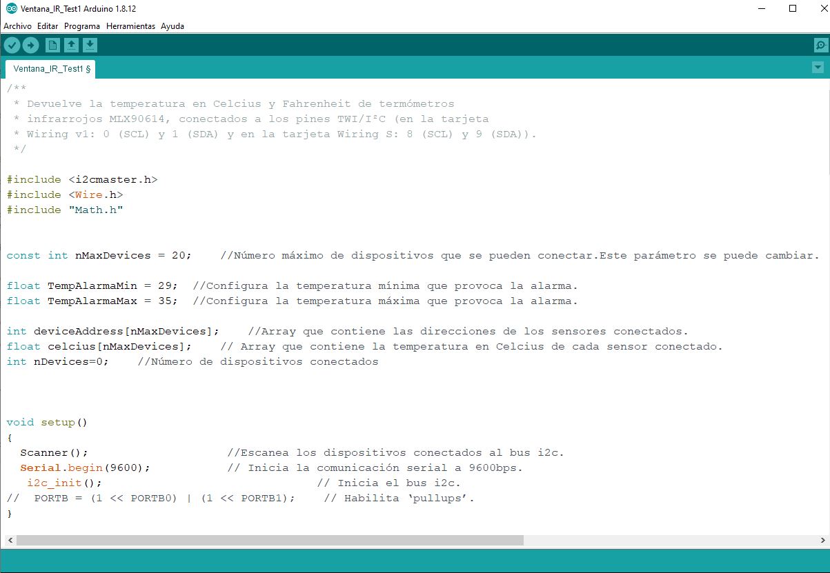
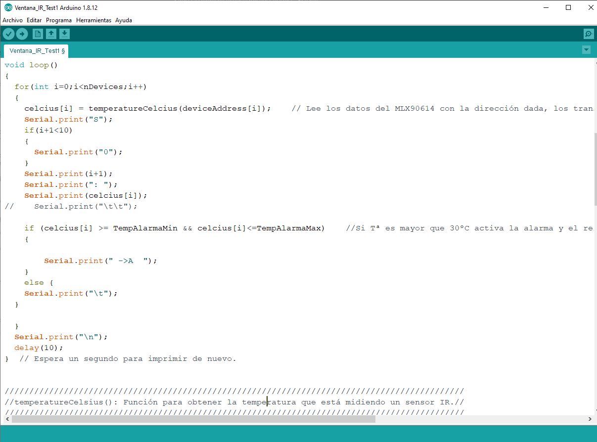
At this point I did the test and the result was satisfactory as seen in this video.
The sensors read the temperature and follow the set point of the programming code.
The Arduino IDE programming code is available for download in section 10.C of this assignment along with the rest of the files created for the development of the work done this week.
10.B. GROUP ASSIGNMENT
The Group Assignment page is at the following link.
In Spain we are still in a state of health alarm and we cannot access the FABLAB.
Álvaro and I communicate by videoconference just as we are exercising our tasks that can be attended by teleworking.
For this group assignment, which consists of “Probe an input device’s analog levels and digital signals” we are going to use as object of study one of the devices that Álvaro will use in his final project as Output, since Álvaro He’s leading this part of the job more advanced than I am right now.
The selected device is the microphone of Álvaro’s outputs board an analog signal, we cannot access the building where the oscilloscope is, but we have been able to see the signal through the Arduino IDE serial plotter, as we have shown in the Álvaro’s individual assignment (link). The microphone generates an analog signal with a waveform from 0 to 3.3v that the microcontroller reads, it applies the Fast Fourier Transform (FFT) to separate the signal into frequency bands, and using the SerialPlotter we can see each band represented by a color.
The result can be seen in the following video.
10.C. Files to download for this assignment
- EAGLE file:
- Board PNG files:
- Programming: