06. Electronics Design
This week, we are mainly learning how to use Kicad in order to: - understand how to use Kicad - how circuits function - how to choose components & create circuits - how to use the circuit files & turn them into PCB
I had spent this week confined due to contact with COVID19. Luckily, I wasn’t sick, but I had to produce from home.
That meant that I had to pick up a CNC milling machine from FabLab. Our instructors are so considerate helped me prepare all the material needed in no time.
Through this documentation, I will be talking about all the process I had to go through starting from understanding what is a an electronic circuit all the way to soldering my final pieces.
Basics of Electronics
In order to understand how to make my board, I needed to get the hang of the basics of what electricity is, its different values, some main formulas as well the role of different components.
I really recommend this KhanAcademy course to understand the basics of electrical engineering.
But here are the main things to keep in mind.
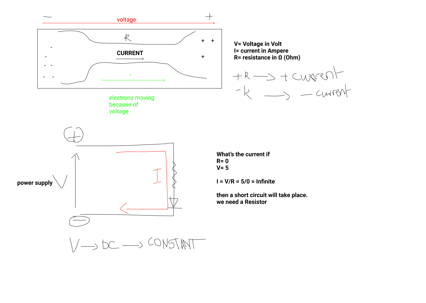
-
The current (in Amps)is the amount of charged electrons (e-) that flow in a conductive material, in most cases, copper. The current starts from the positive pole (GND) due to convention, we call it conventional flow. But in reality, the elctrons are moving from the negatively charged pole to the positively charged one. The current flows along a conductor trying to fill a void wherever there’s a depletion of electrons -
Voltage (in V)is the force or pressure that is responsible for pushing the charge in a closed looped conductor. It is the electrical pontential between two points. -
Resistance (in Ohms Ω)is how resistant a material or component is to the flow of electrons. The more resistance there is, the less current there is. -
one very important law to keep in mind in order to calculate the values of our circuits is the Ohm’s Law:
V= I x R V is measured in V, I in Amps and R in Ω.
Micro-controllers and components.
This chapter will definitely not be as detailed as the amazing documentation provided by FabLab Barcelona
But I will try my best to put together all the information that I would like to be able to go back to in case of doubt.
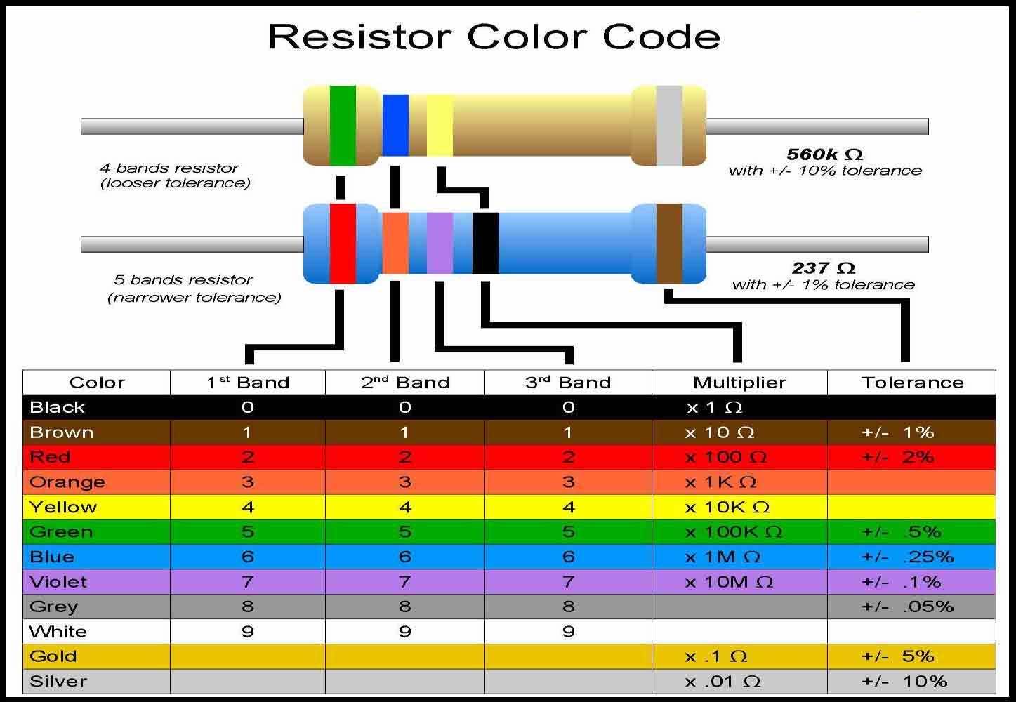
Resistors
In electronic circuits, resistors are used to reduce current flow, adjust signal levels, to divide voltages, bias active elements, and terminate transmission lines.
Check out this ressource to understand more about resistors. And this one or this one to calculate the value of your resistor.
Capacitors
They allow to store electricity . I could be polarised or non polarised
Capacity is a very complex thing to measure because pacing the capacitor on a specific material can alter it capacitor for the purpose of filtering. we can play with the capacitance of a material in order to manipulate the flow “timing”.
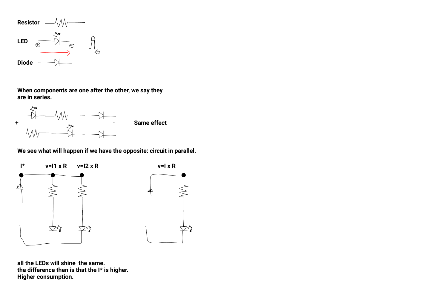
Diodes
conduct the current in one direction.
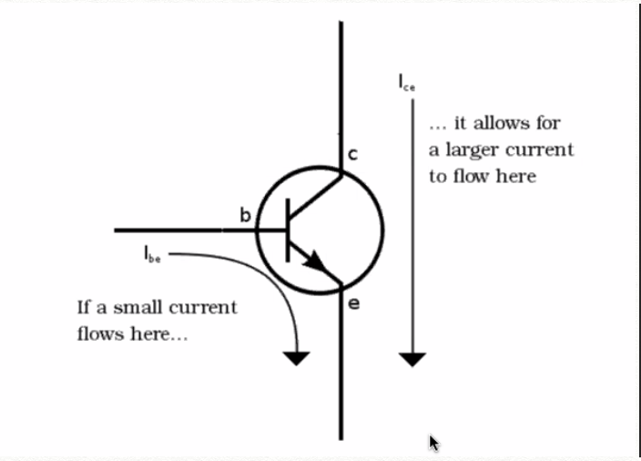
Transistors
Transistors behave like small switch that are able to to control a small current flow with a very large current.
Mosfet are more sofisticated transistors.
Kicad
Kicad is an open-source software that allows to create electronics circuits using footprints & symbols libraries. Within Kicad, there are several steps to follow.
Managing libraries
It is crucial to manage both symbols and footprints libraries.
-
Kicad Footprint libraries contain several
.prettydirectories. Each directory contains several.kicad_modfiles. -
Kicad symbol libraries have a
.libextension. They are usually accompanied by a.modfile with the same name.
Both Kicad footprint libraries and kicad symbol libraries should be synchronised.
Within the contexts of FabLab, this library is very useful because it includes all the fablab components.
Designing my PCB board
I’ve decided to design & produce the PCB parts to make a pomodoro, inspired by the work of Antoine Jaunard.
Working on an already existing board helped me understand the differences electric components and how they connect together.
Since I do not come from any engineering background, and getting the hang of the current classes was too all over for me, I decided to understand by following baby steps on KhanAcademy
Also, this link made me understand Microprocessors a bit better.
This is the list of components I will need to make my Pomodoro:
- Micro-processor AtTiny 1614
- UPDI & FTDI to program, which I later realised can be put into one piece.
- FTDI to program 4.. 4 LEDs & 4 resistors, one resistor for each LED (3 of them are green and 1 is red)
- two switch with two resistors, one resistor for each switch
- Capacitor to make sure everything is going fine.
Choosing my resistors & my capacitor calculations
Using the fab lab inventory, I chose the resistors that had the closest values to my calculation result.
The idea is to first calculate the resistance my LED and switch need, then substract it from the resistance of the overall circuit it.
V= 5V
According to [this datasheet](http://www.digikey.com/products/en?keywords=160-1169-1-ND%09/)
the green LED has the following values:
V= 2.1V I= 0.01 A

That leaves us with the Vresistor = 5 - 2,1 = 2,9 V

To calculate the resistance needed from the
resistor of the green LED, this is the math I did:

V   = I x R
2,9 = 0,01 x R
R = 290 Ohm

This result is the value of the resistance that each resistor needs to take care of in order to make sure my components don't burn!
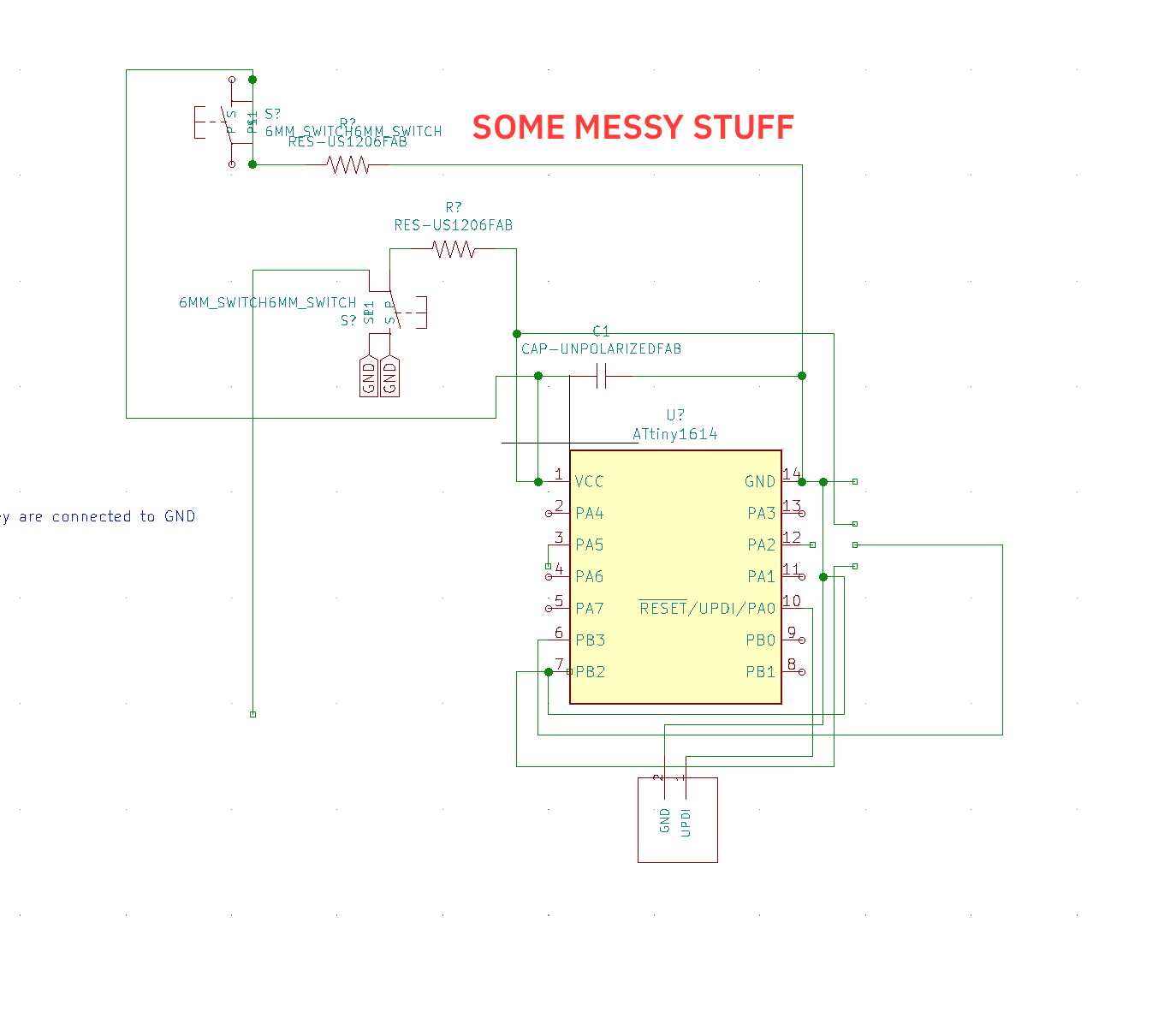
Schematics: EEschema
Eeschema is a sub-section of Kicad.
It allows us to place components & connect them together.
the file is already saved within a folder with .sch extension
-
In terms of components, it is very important to choose the ones with the correct
footprints. The footprints we are using for this assignment are the Lab’s to make sure the circuit we want to mill is compatible with the components we have at the lab. -
EEschema also allows to change values and references of components used, which comes especially handy for more complex electronics.
-
Components can be either dragged or moved. Moving disconnects all connections already established. Dragging maintains those connections.
-
Placing Components
Here are some of the shortcuts:
Rto rotate the componentCto copy itMto move itWto draw a wire
I start off by placing all of my components on the board. I make sure that they are all components that are linked to the Fab Library, previously loaded into Kicad.
- Connecting components
There are multiple ways to create the circuits on the EEschema.
I chose to use tags because it is visually easier.
As I place my components, I first make sure to connect the GROUND to the GROUND and the VCC to VCC.
VCC stands for voltage at the common collector.
It is usually the positively charged energy input.
GND stands for ground.
It is the reference point from which voltage is measured. The return path for electric current back its source.
For the rest of the connections, the Attiny 1614 datasheet helped me understand the connections that i needed to make.
I made sure to understand why I am doing what I am doing as I was working.
That’s why I have decided to group the series of components in separate boxes and use tags.
- Netlist
The netlist file is saved in .net extension
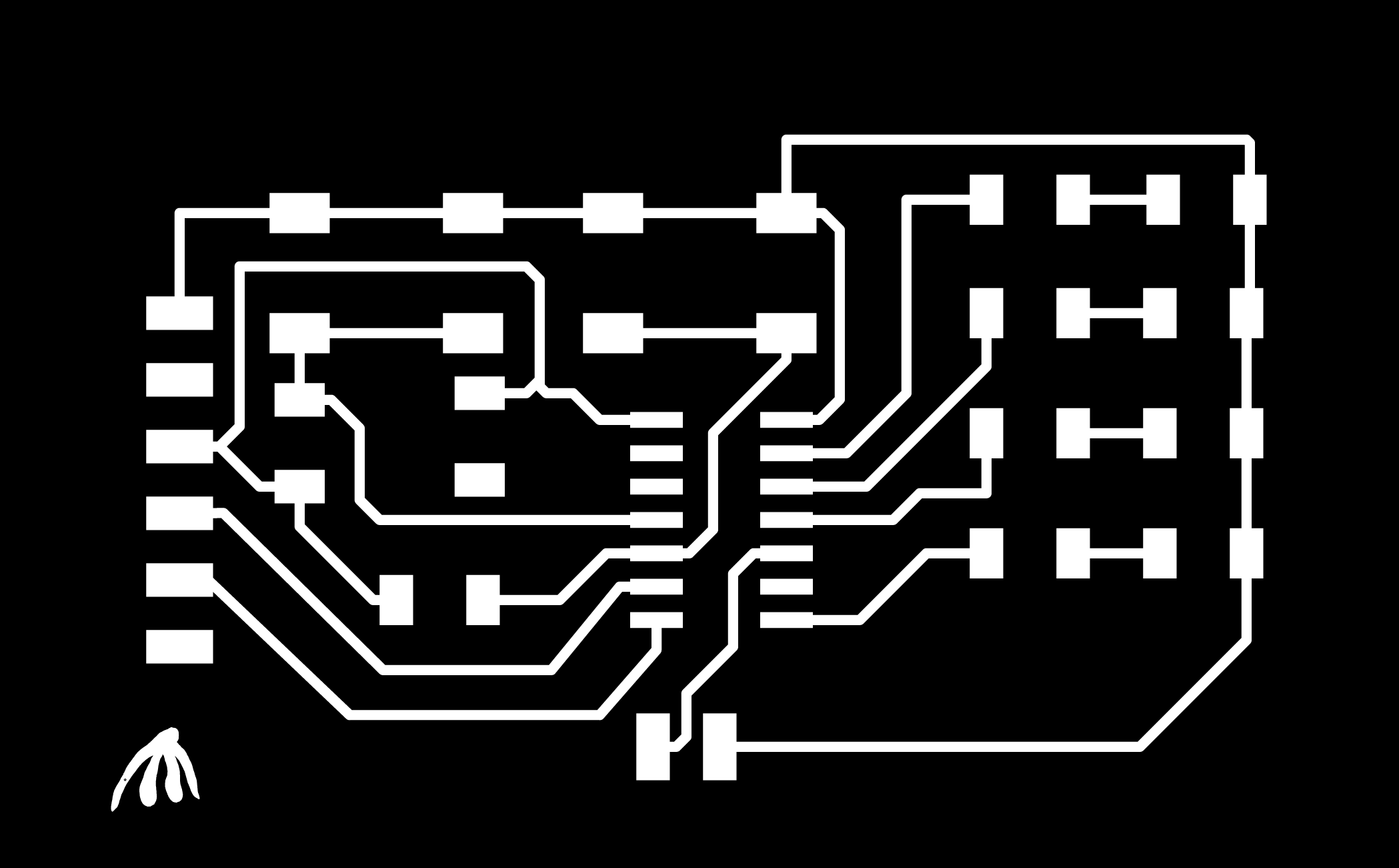
PCBNew
- To create my PCB print, I import the netlist file created into
PCBnew
It usually checks all the components are linked to the library.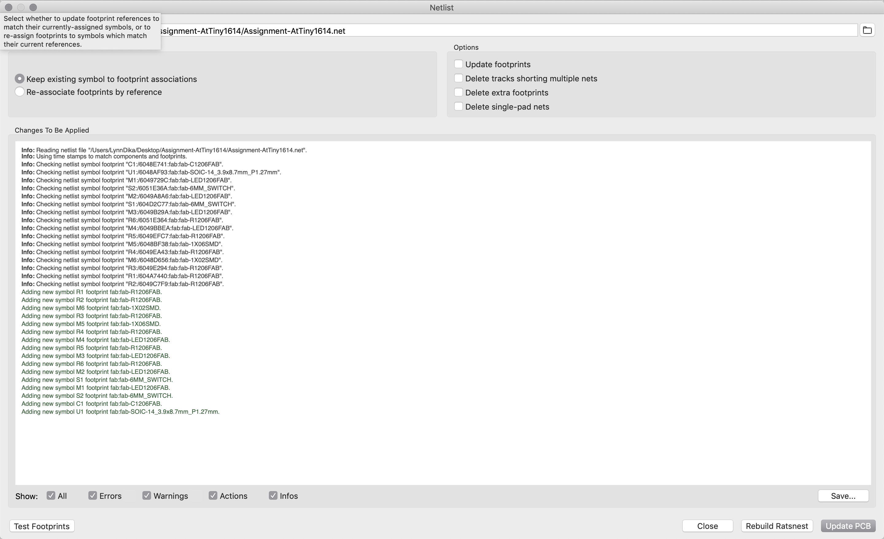
It opens the following file.
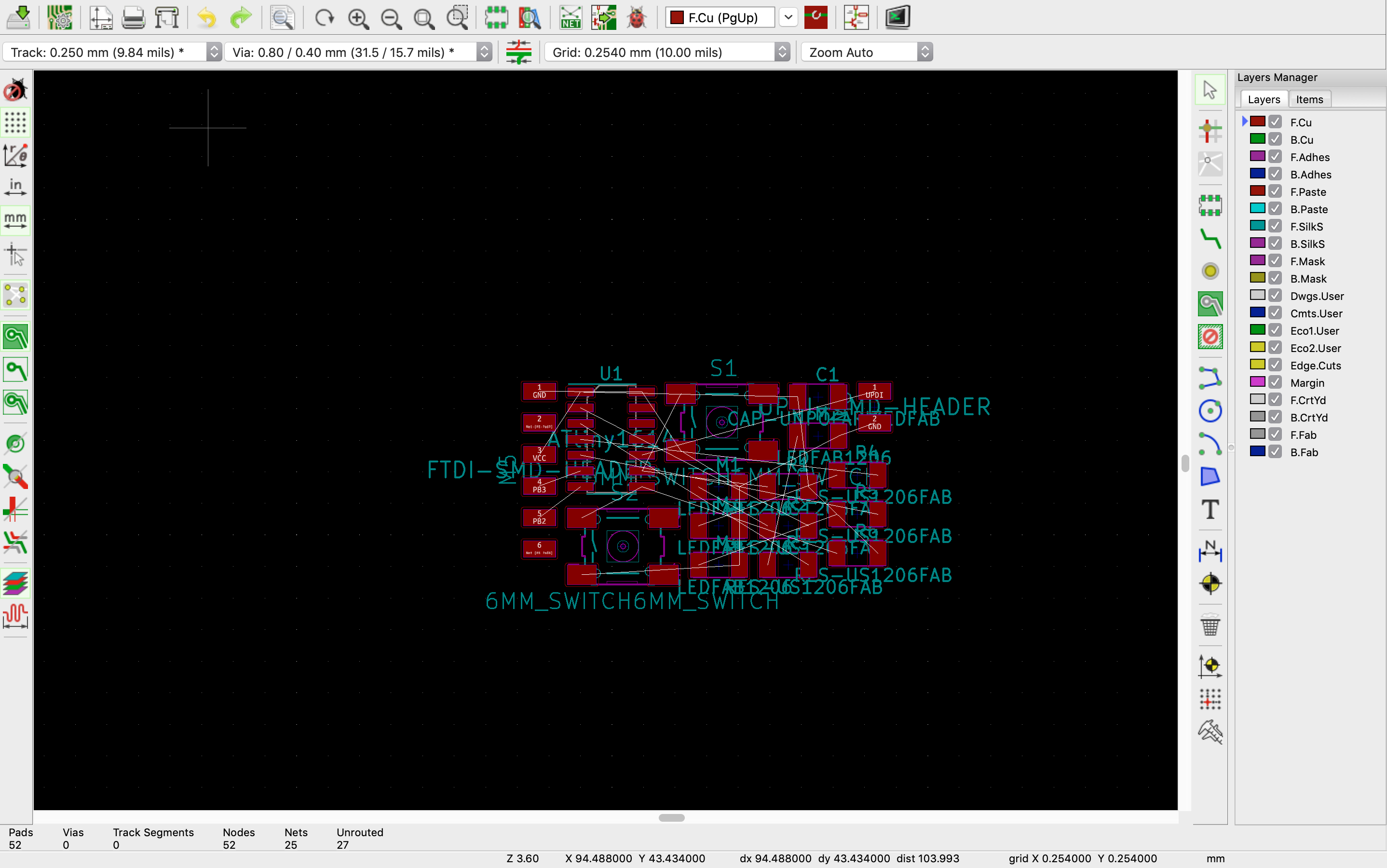
Connections
The white lines define the connection I had previously made in EEschematics. The idea is to connect them by making the shortest pathways to keep the current flow fast. They are a reference, not a bible.
- Starting with the connections to the programmer is a good idea.
- Making sure to connect the GND ultimately is a good idea as well, as it connects all the components together.
- Rotate the components as much as you please to make the connections make sense.
- It is also very important not to fall into the trap of having connections criss-cross each other.
- It is better not to have nodes and to connect in a way that does not create any weaknesses to the traces.
- By creating a circle with the diameter of the end-mill we are using, we can manually test the distances between paths to reduce risks in milling.
It took me a couple of hours to link it all together, and a couple of sneakpeaks to antoine’s documentation.
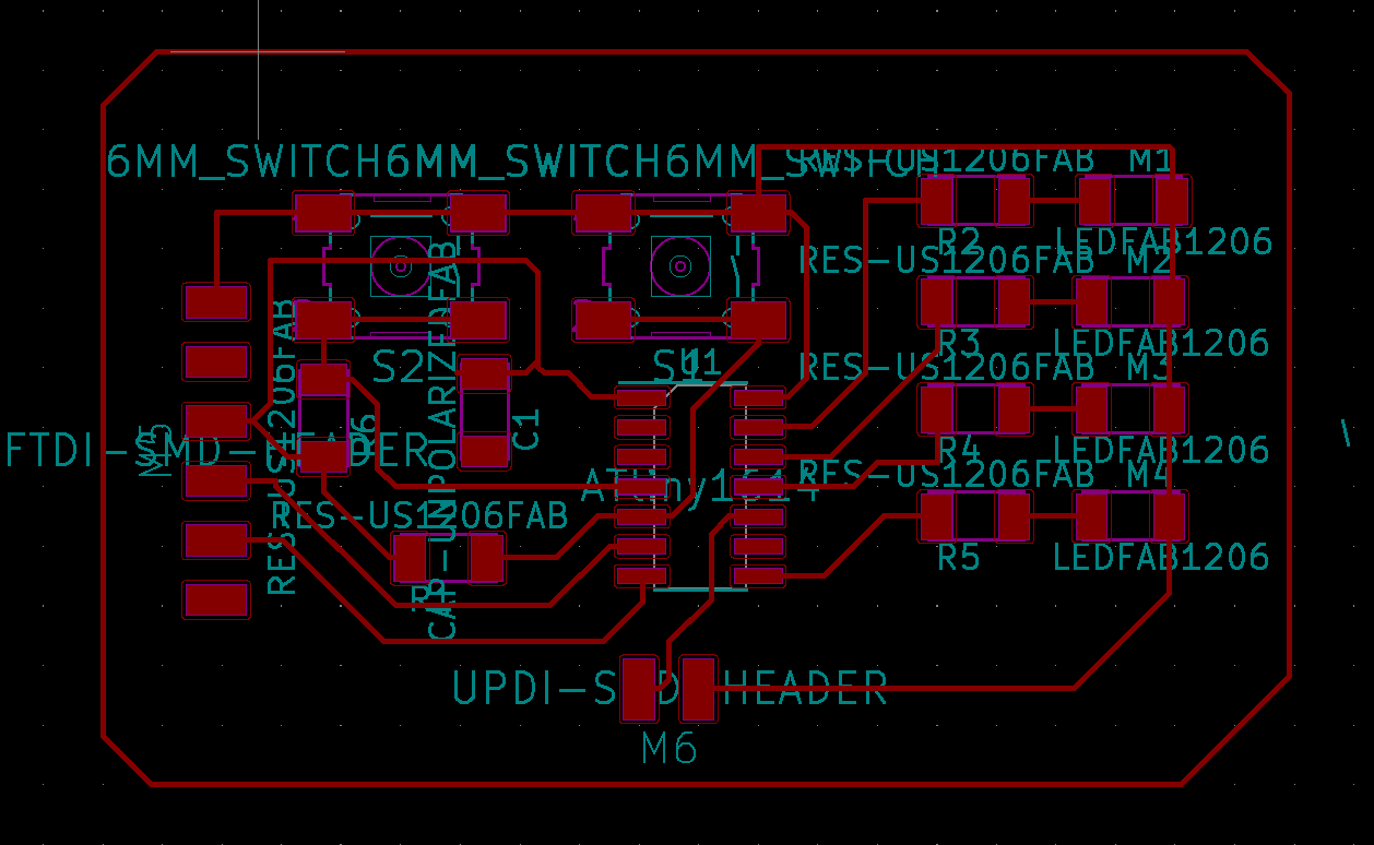
Layers
Layers have the different representations.: the aqua f/silkS green is the name and values. the red layer is the front copper . the green is the back copper.
F is used to flip from one side to the other.
When we have holes, it is represented with the colour yellow.
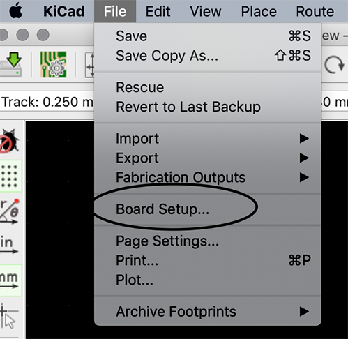
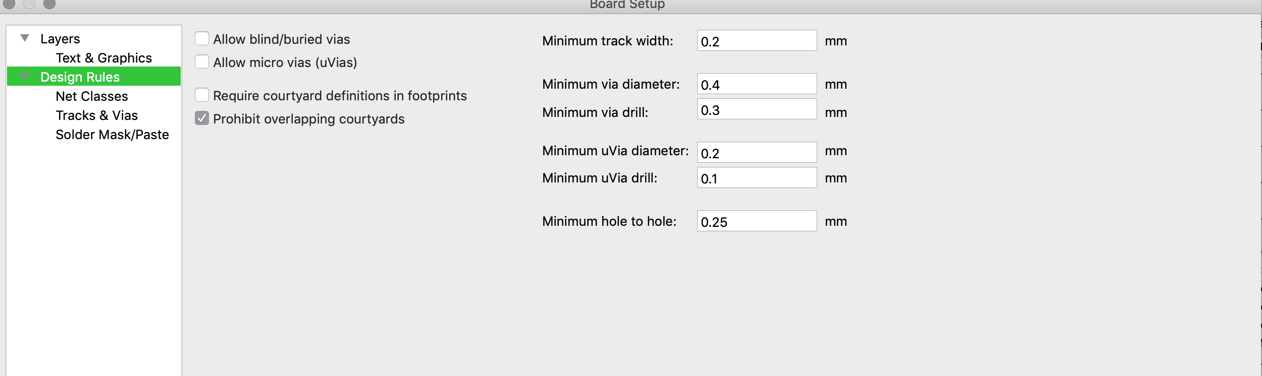
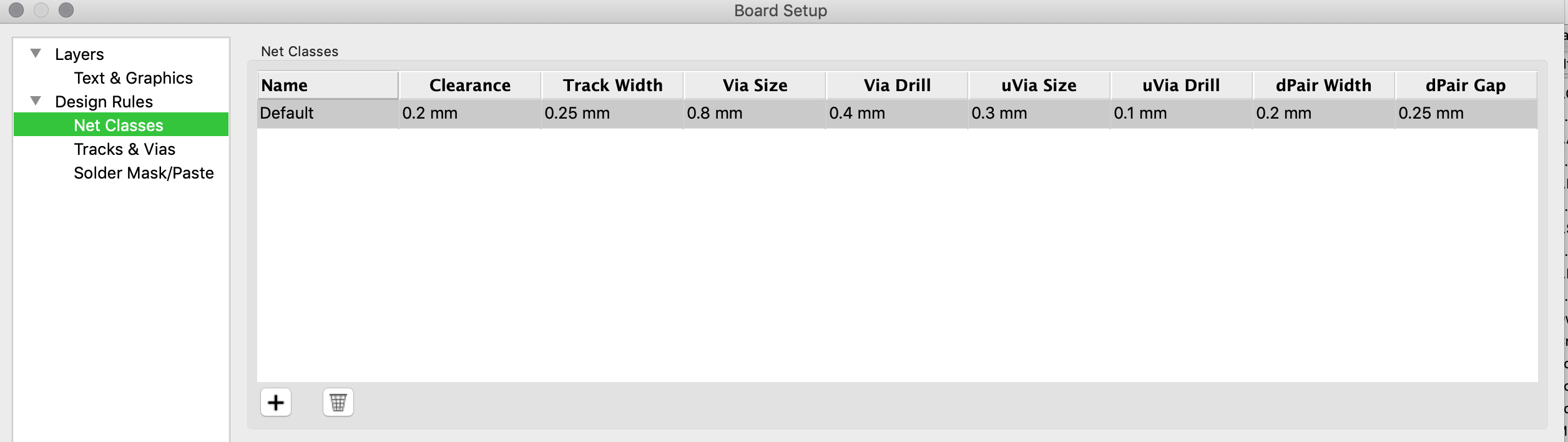
Design Rules
After successfully designing my PCB, we need to export the file under the right conditions. I needed to make sure that the thickness of the trace is correct. Clearance 1/64 = 0.4 mm Track Width 0.3mm is recommended.
We can calculate the track width by going to the PCB calculator
Here some design rules I found online.
Those design rules can be checked by entering to the following page.
Export for manufacturing
After exporting to .svg, I opened the file as it is in illustrator in order to fix any over-lapping or overly thin traces. I then created two layers, one to export the file for the exterior trace done with the 1/32 mill & another layer for the interior traces done with 1/64 mill.
I saved the .png at 1000 dpi resolution.

I then exported into .png mode to upload to
Fab Mods
or to Mods Project
Once the .nc was generated, I set up the whole milling process.
Since I was confined out of precaution during this time,
I was lucky enough to use Sain smart Genmitsu CNC router at home.
Using Candle GRBL
I had to download the mac version of Candle GRBL
Candle is quite simple to use.
First, I had to go into settings, and connect candle to the USB port that identified the CNC machine.
Then, I had to adjust the spindle speed maximum.
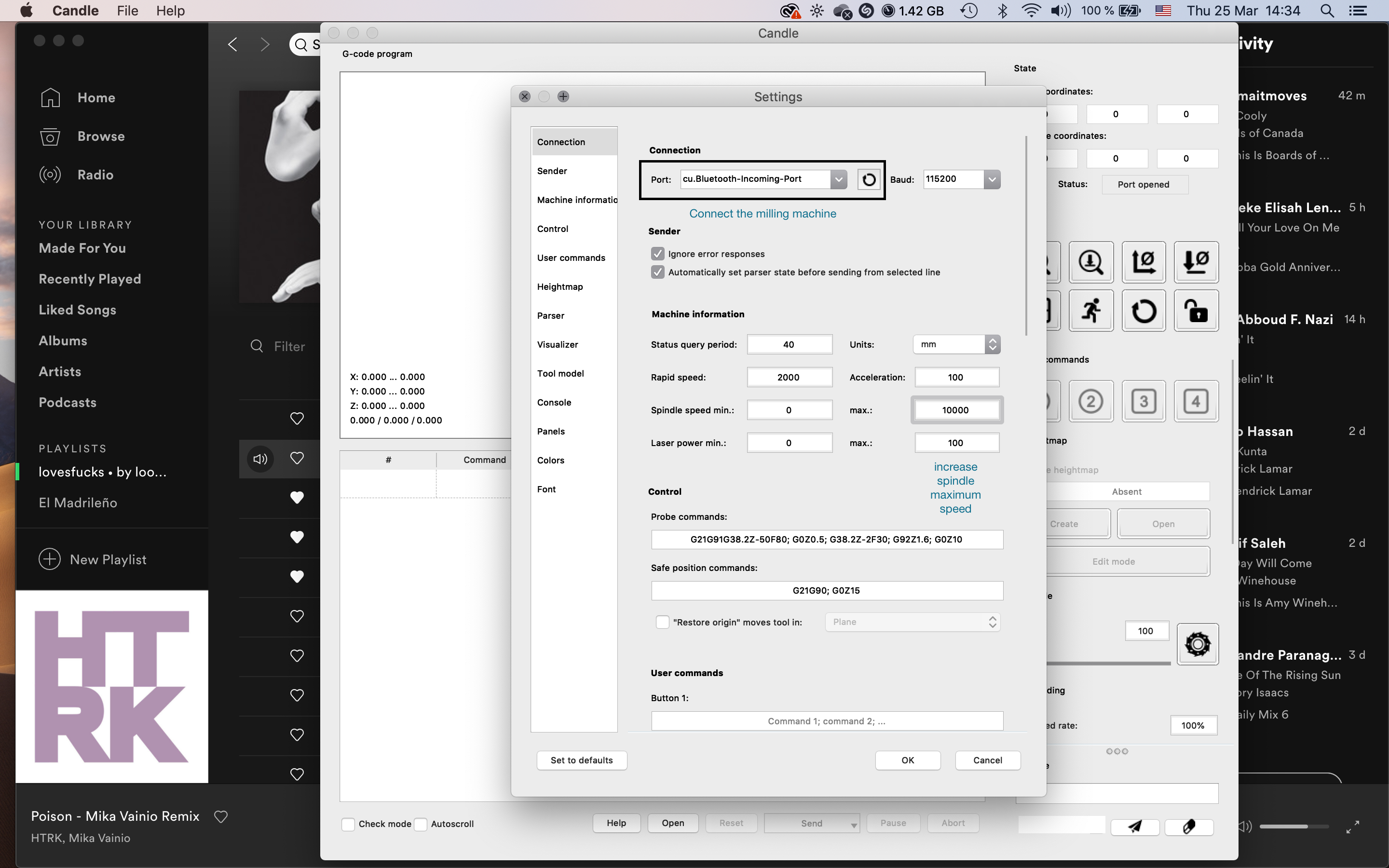
Setting up the X & Y axis was quite straight to the point. As you can see on the software, the button to allocate it is very self-explanatory. My instructor, Eduardo, had provided me with this tutorial that made things quite simple.
The main challenge is to set the Z origin. To set the Z home, I needed to spindle the mill and bring it down carefully, at the rate of 0,1 until it touches the board, and then set the Z home.
I had to give it many shots. As you can see below.
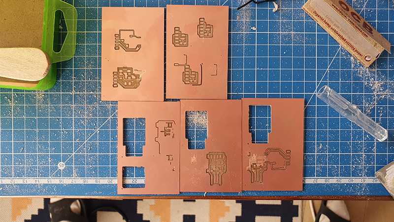
Since the way to change the endmill is manual, I was first doing by eye. By that, I mean I was manually calibrating the X, Y & Z axis based on the engravure of reference I did for the internal traces.
But then, after seeing the interface the Candle, I realised that maybe i can send a code command to the machine to relocate to its point of origin for the X & Y axis, and then calibrate the Z manually.
I had written this line of code
G0 X0 Y0 F10000
Things to take into consideration while milling
-
Make sure the edges of the double-tape you are using to stick the copper are outside of the board itself. That is to make sure the board is flat, this is important because we are talking about milling with a few mm of depth. You can cut the edges of the double-tape later.
-
Measure your board and in which direction of the board it fits. I had made a couple of cuts that wouldn’t fit, or would overlap with failed milling since I didnt pay attention.
-
When setting the Z, the mill should touch the the copper board just the right amount or that might geopardize the thin traces.
-
If the copper board is unilateral, make sure that the milling is clean by putting it facing a light source.
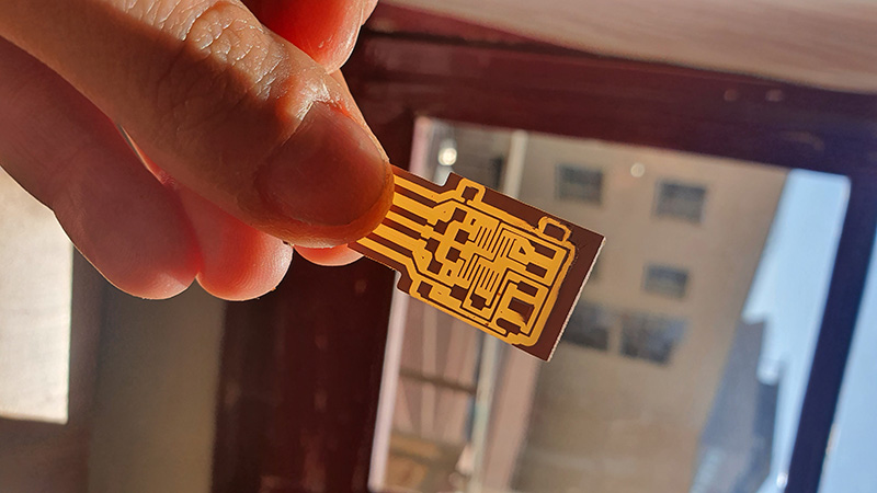
Things to take into consideration while soldering.
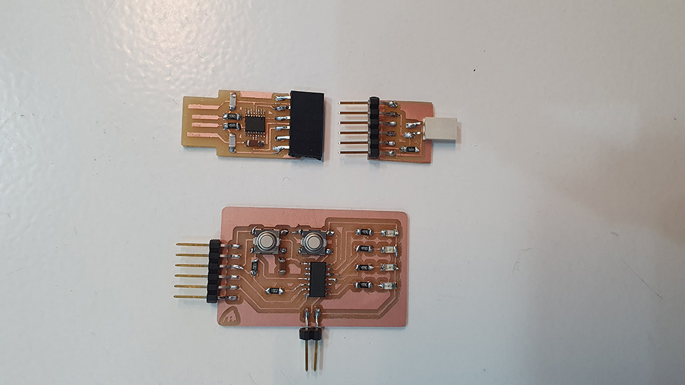
I had to mill & solder my pomodoro, an FTDI, and a UPDI. This was tricky considering the amount of time I had, but it was a great learning experience.
Some of my tips are:
- Solder by putting the iron first, then the soldering wire on top of it.
- Remove any excess solder to avoid short circuits
- Be patient.
- Make sure that you place your components in the right direction.
For my AtTiny1614, I had to find the miniscule dot that marks the VCC to know how to place it. The datasheet schematic helped me with that.
For the LEDs, I realised I needed to find the green line that indicates the negative side to connect it well.
This is the result of my work. No short cirucuits, all checked with a multimeter. The way LEDs light up to check their working is kinda cute.
I will be documenting how they work in the Embeddeded Programming assignement.
Update: ALWAYS MAKE SURE YOUR TAGS ON YOUR SCHEMATIC ARE WELL CONNECTED.
While in embedded programming week, i realised that my capacitor is not connected to ground. That was because the tag in the schematic was not well placed, which led to the white line on the pcb indicating the connection to ground not appearing.
I will fix this with an external cable due to time limitations.
Working files
Kicad files + Illustrator [CN files for milling] (Pomodoro-trace.nc.zip) Updated Kicad file with capacitor connected to GND
Learnings
- Don’t drink too much coffee or have too much sugar before soldering
- Print and put somewhere clear the main formulas to keep in mind.
- ALWAYS keep in mind the current, voltages and resistances especially for more complex projects to come in the lab.
- Another thing to keep in mind is the memory capacity of micro-processor.