5. Electronics production
Assignment
- Group assignment:
Characterize the design rules for your PCB production process - Individual assignment:
Make an in-circuit programmer by milling the PCB, check if you can program it.
Group assignment
Our group: Lucasz , Gleb, Marjo and I.
Used machine
The design rules are tested with different milling pits using the Oulu Fablabs monoFab SRM-20.
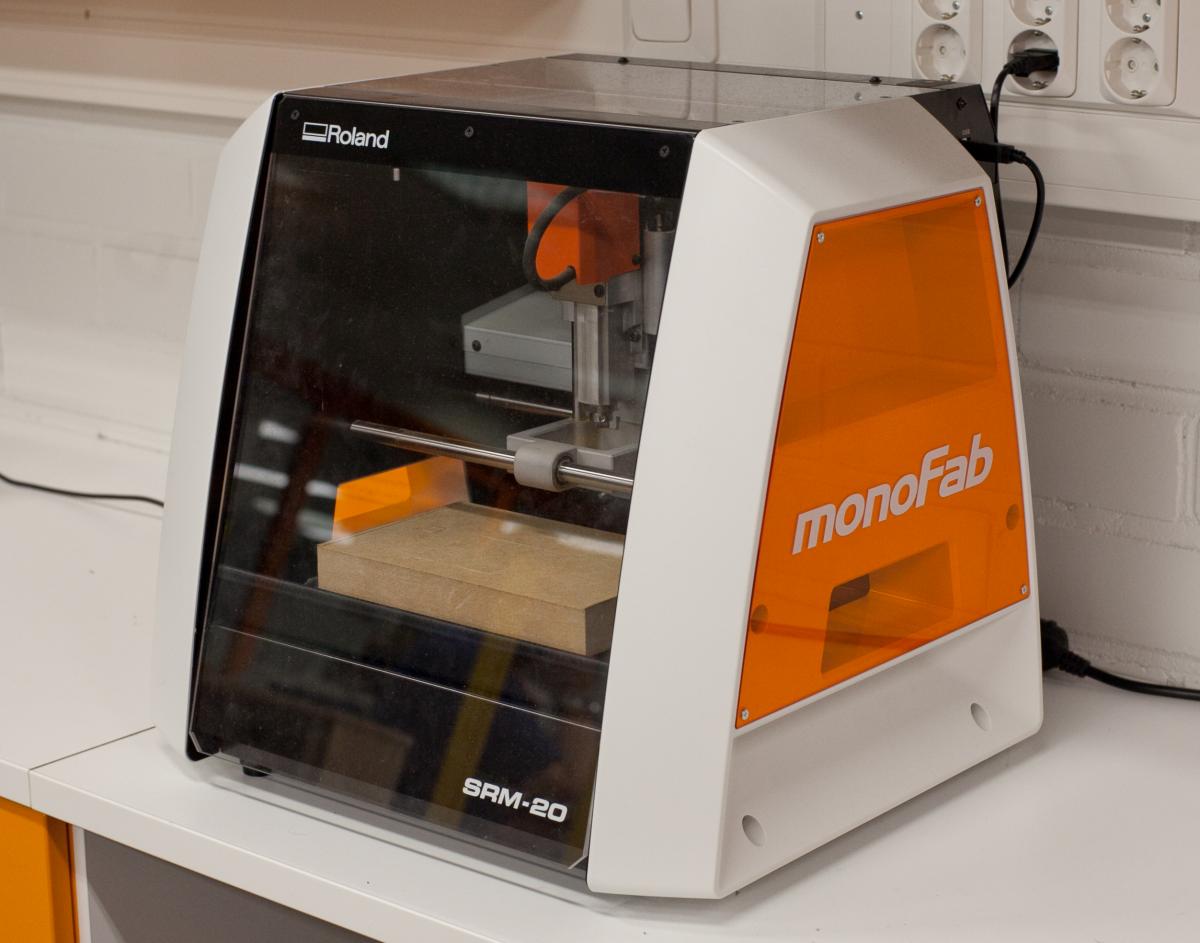
The Roland milling machine specification.
| Model | SMR-20 |
|---|---|
| Cuttable material | Modeling Wax, Chemical Wood foam Acrylic, Poly acetate, ABS, PC board |
| Cutting Tool Chuck | Collet method |
| Distance From Collet Tip to Table | Maximum, 5.15 in, 130.75mm |
| External Dimensions | 451.0 (W) x 426.6 (D) x 426.2 (H) mm |
| Mechanical Resolution | 0.000998594 mm/step |
| Operating Speed | 6 – 1800mm/min |
| Spindle Rotation Speed | Spindle Rotation Speed |
| Workpiece table size | 232.2 (X) x 156.6 (Y) mm |
| X, Y, and Z Operation Strokes | 203.2 (X) x 152.4 (Y) x 60.5 (Z) mm |
Mods

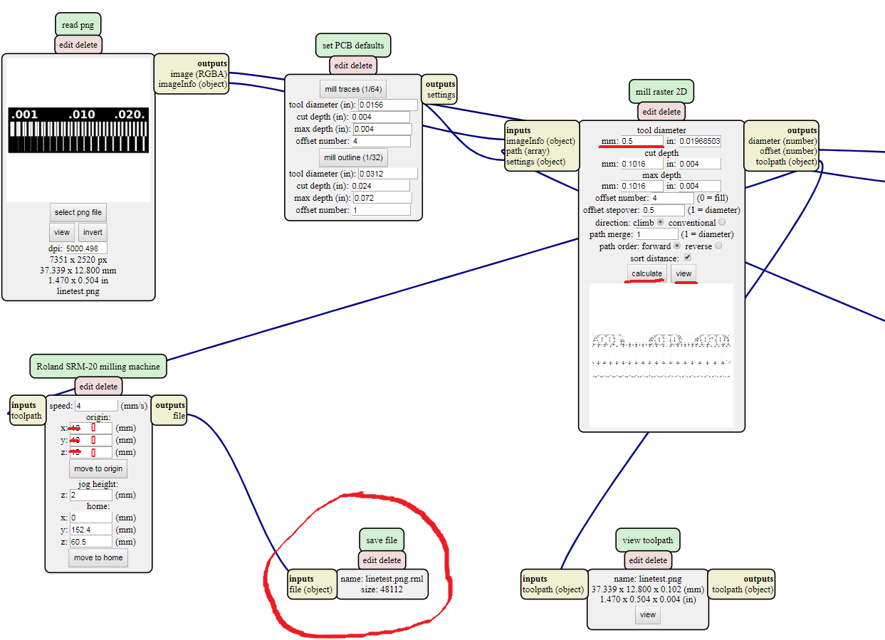
From the image a milling program has to be made. This can be done easily using Mods The milling program is the set of instructions that the machine follows to mill the PCB.
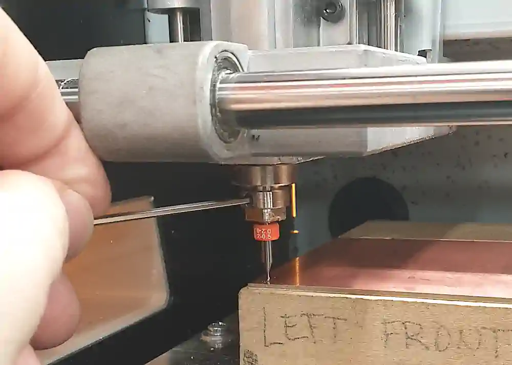
The mill bit is first inserted to the Collet.
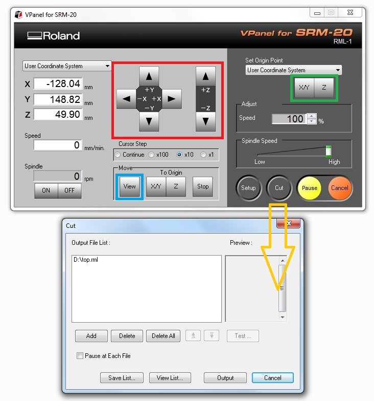
When everything is positioned and reset correctly it is time to press the cut button, marked with an orange arrow. This will bring a window, where the desired file might be loaded. By clicking Add successive files should be added. Mistakes can be corrected with the Delete button. In the end, Save List has to be clicked. The process should be started by clicking “Output”
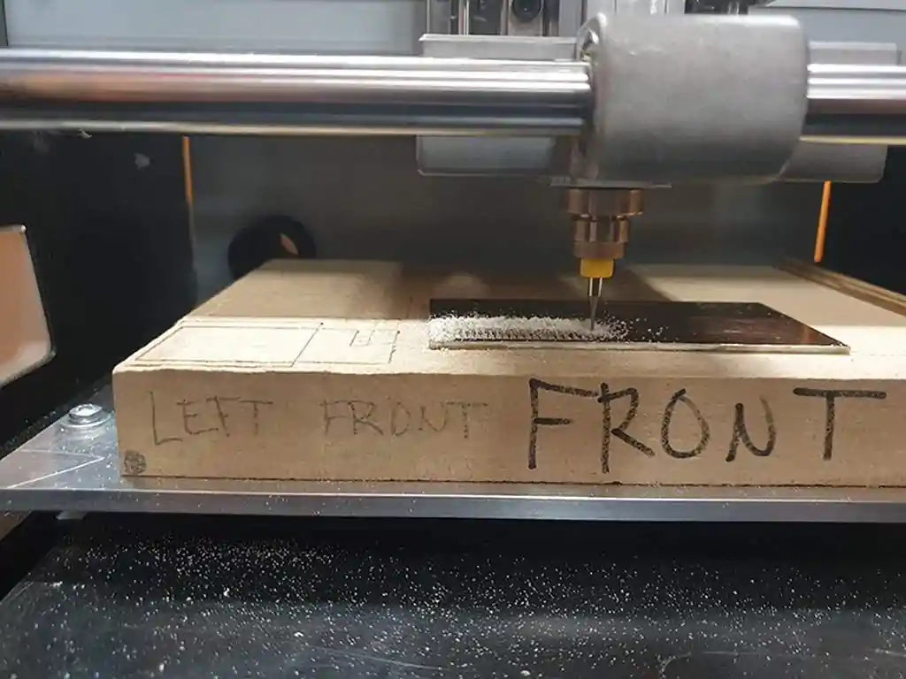
Milling whit the mill
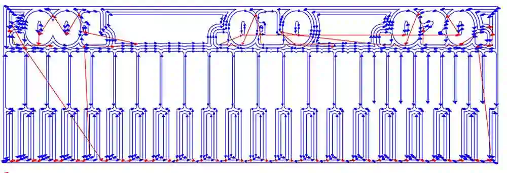
The results for the different milling bits.
Then the outline milling to release the board.
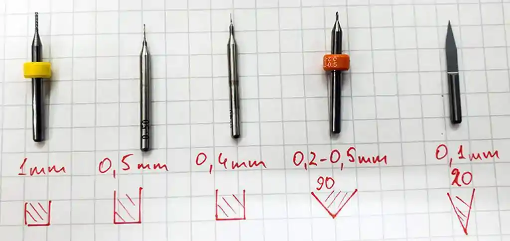
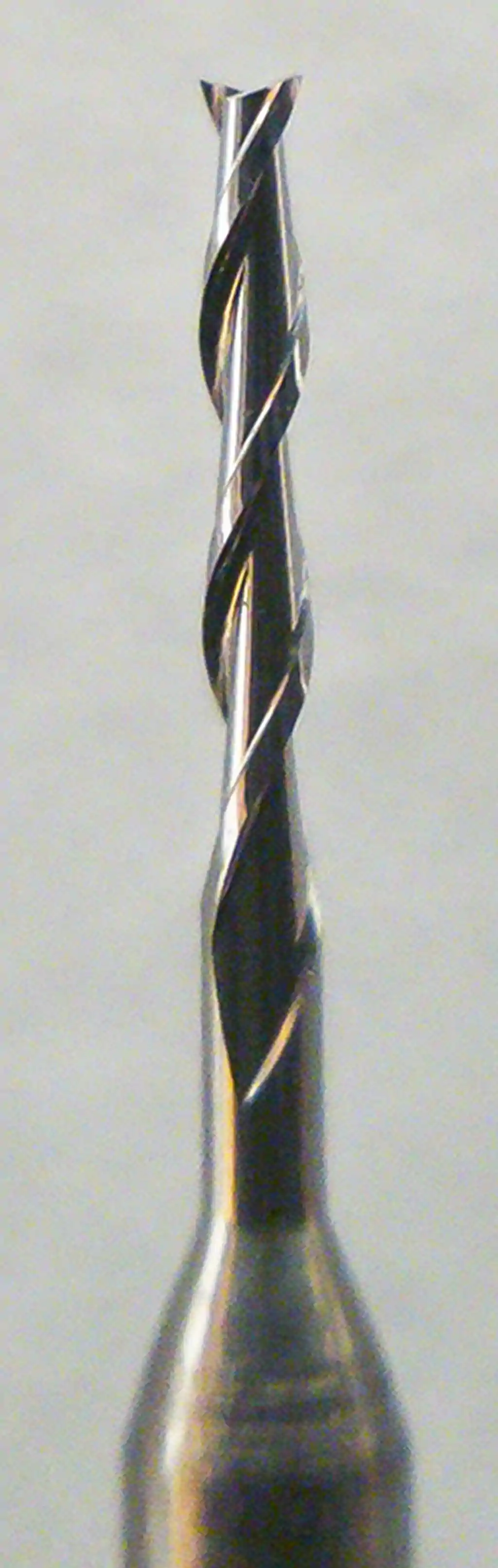
| Result | Tip image | Tip specs |
|---|---|---|
 |
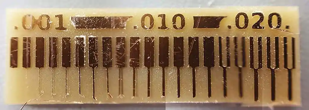 |
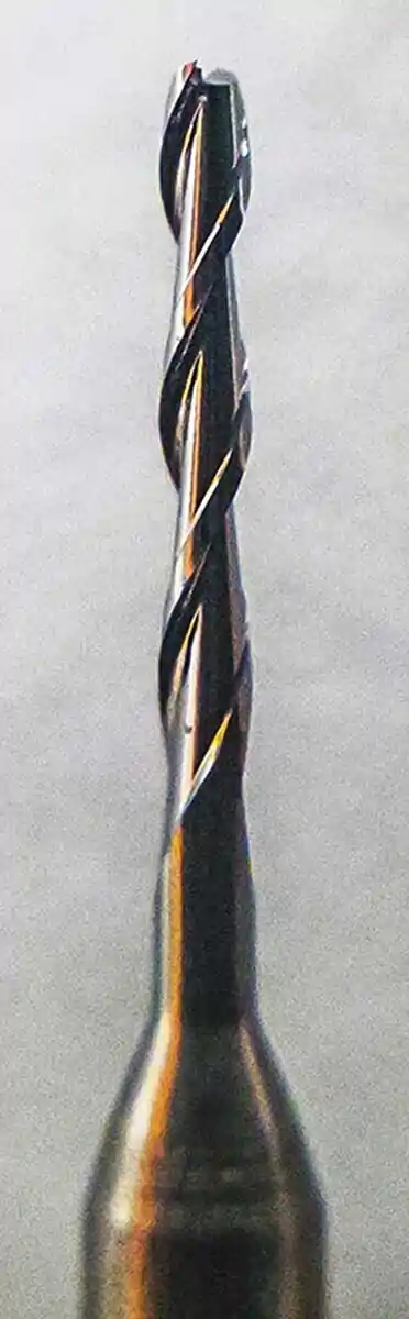
0.4mm endmill. |
 |
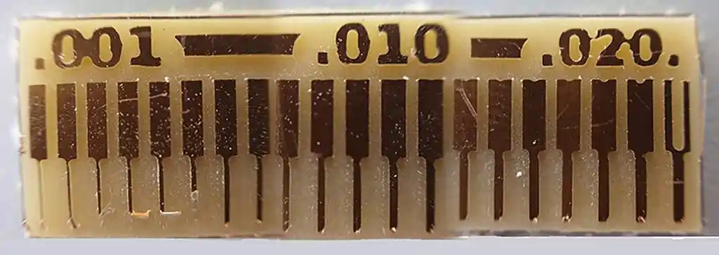 |
0.5mm endmill. |
 |
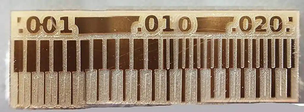 |
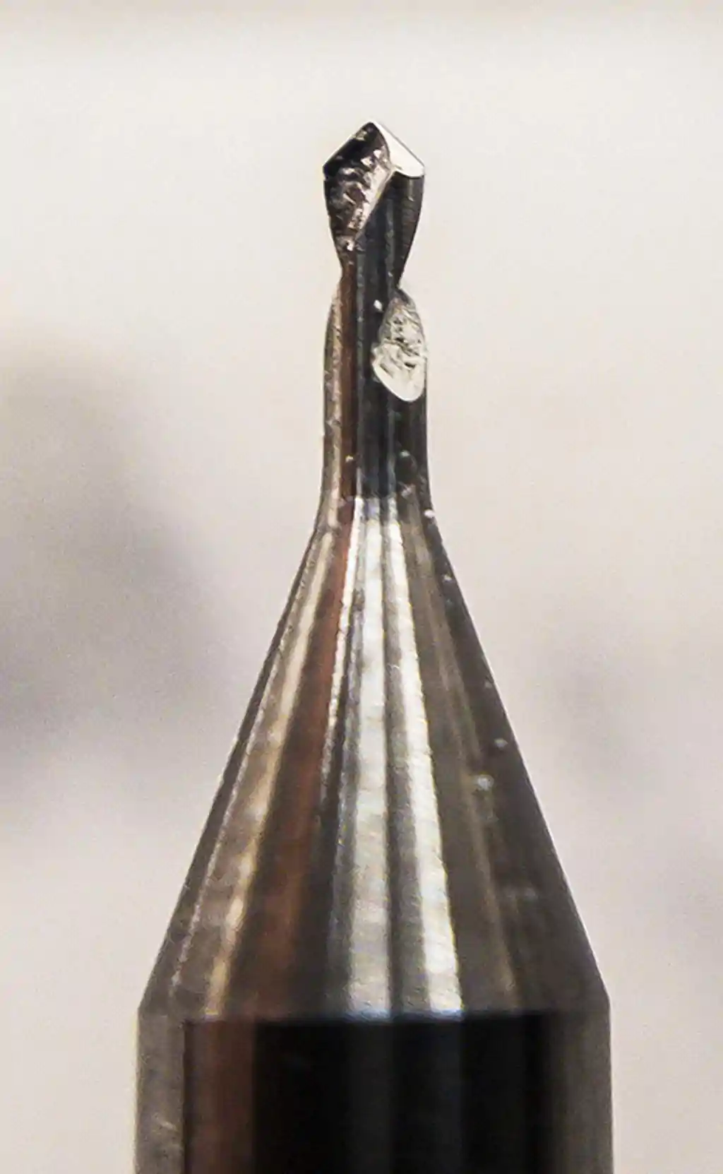
02-05mm 90deg V tip |
The 02-05mm 90deg V tip does the best job. This is used in the individual assignment.
The steps for milling PCB
* Selecting the used milling pit.
* Making the milling program(RML-file) from the circuit image for the milling pit.
* Cutting and fastening the PCB blank into the milling machine.
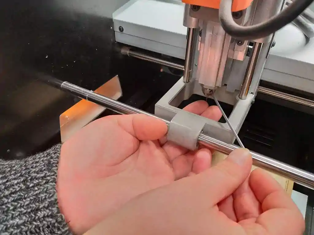
* Carefully attaching the mill pit and adjusting the zero point.
* Load the RML file and start milling
* Change the milling pit for the cut out pit(1 mm) and load the RML program to cut loose the PCB.
* Clean the machine.
* Drill holes(if needed)
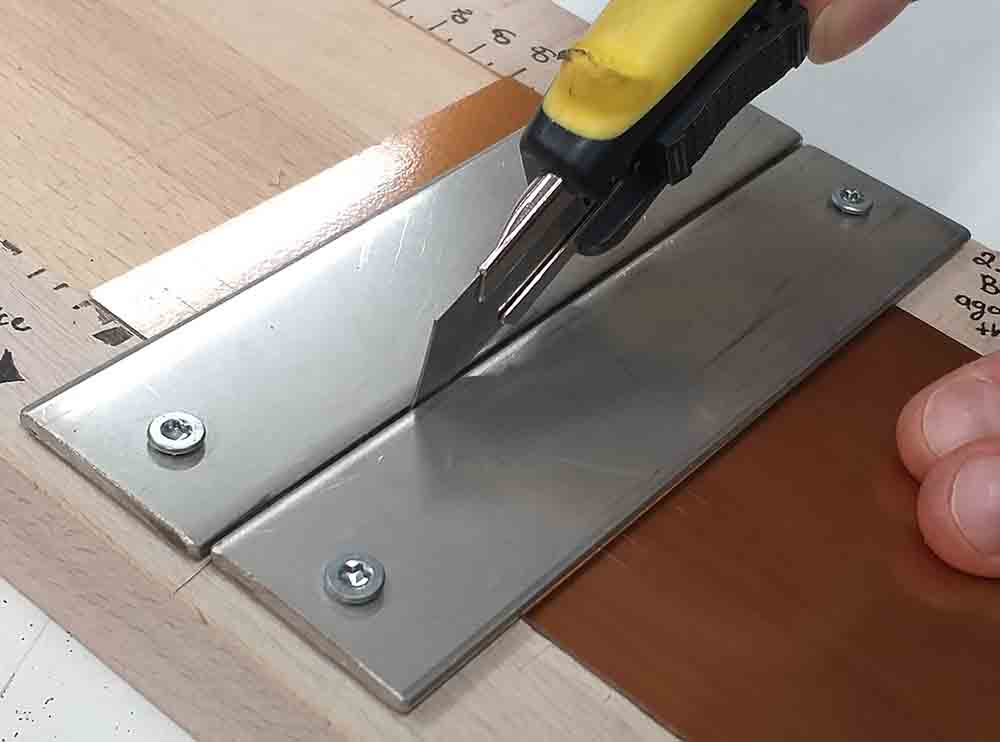
* Clean the PCB. Steel wool rub with isopropanol alcohol.
* The PCB is ready to Ready to solder.
Individual assigment
Selecting the ISP
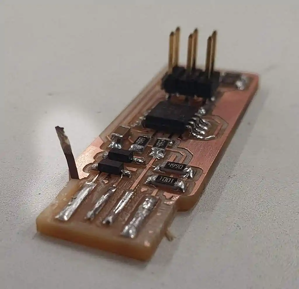
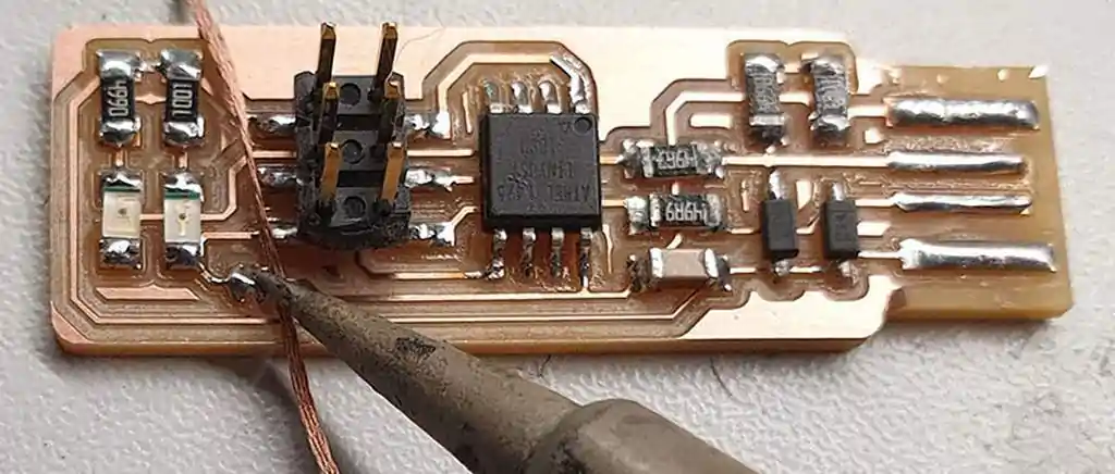
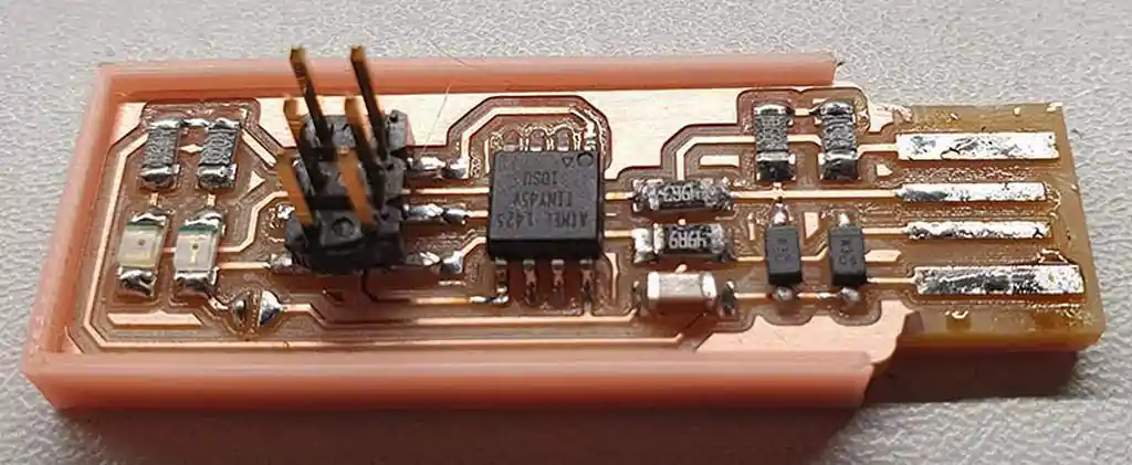
For individual assignment was to make ATTiny 45 based In-system programmer, ISP. The manufactured version was the Brian’s version of the board.
Fabrication method.
For the fabrication method the new Mods was used.
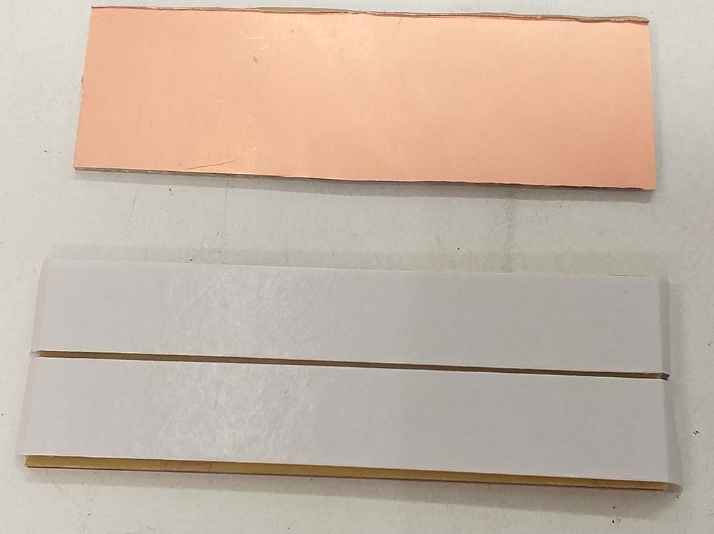
firts the boards traces and the outline cutoff was downloaded.
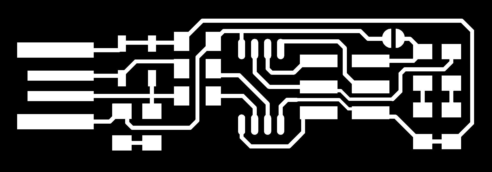

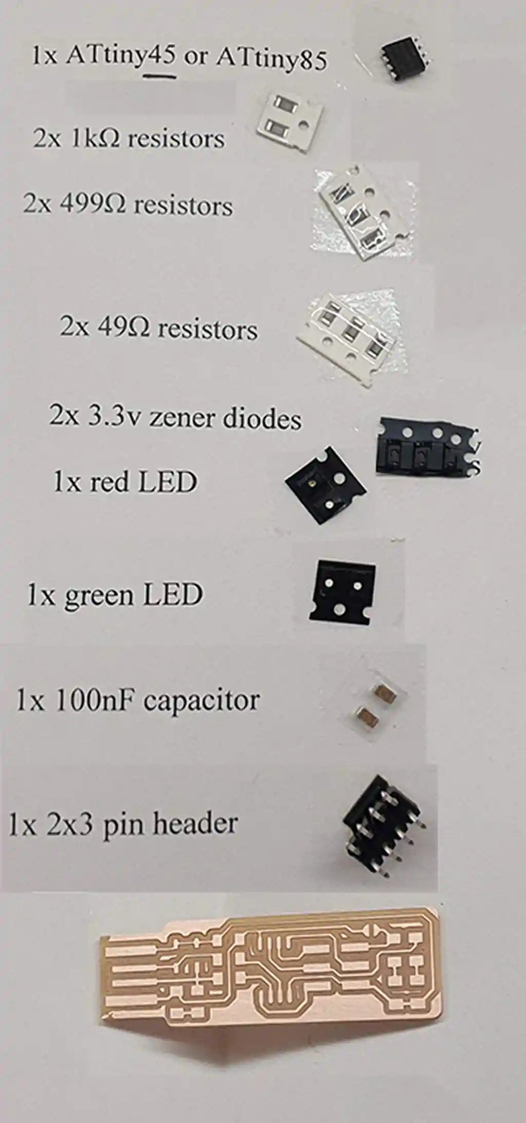
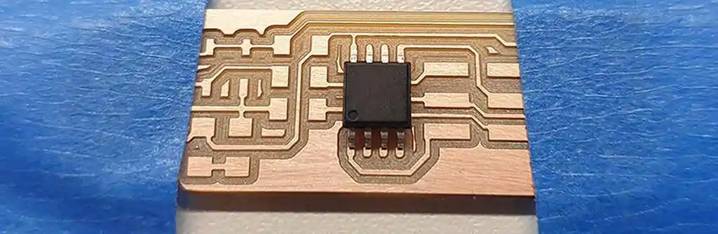
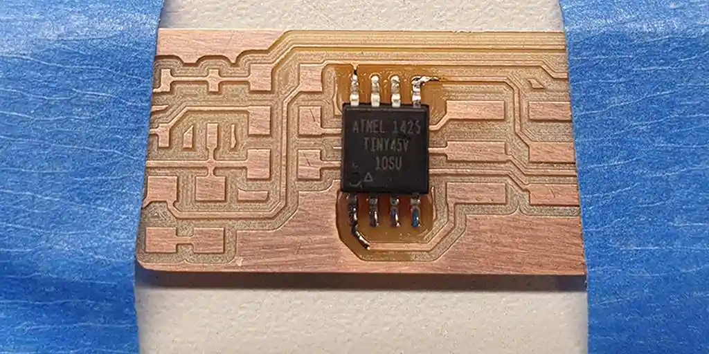
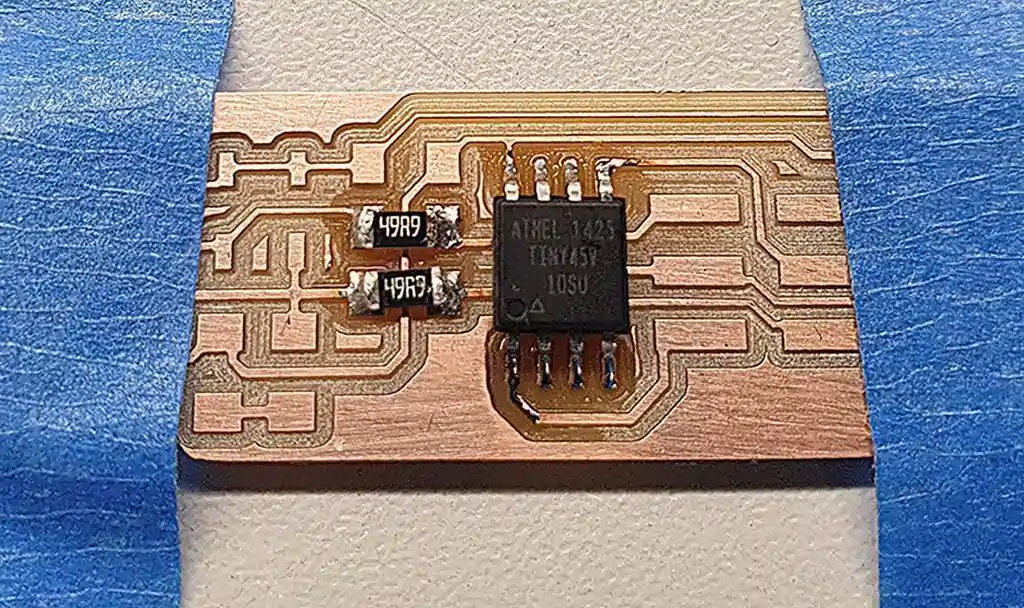
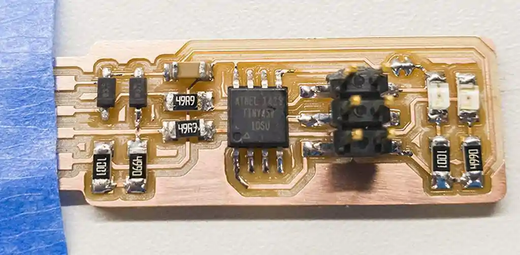
The FabTinyISP consist of Attiny45 and some passive components.


The Mods was used as in the group work and the milling pattern was obtained for the 0.2-0.5 mm 90 degree V - shape milling pit.
The milling of the board was done in the same method as the group work test boards.
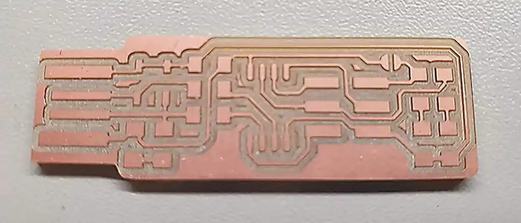
FabTinyISP milled 0.2-0.5 mm 90 degree V - shape. used 0.3 mm trace widht and 0.106 mm cut depth.
Materials needet in soldering.
* 1x ATtiny45 (or ATtiny85) microcontroller U1
* 2x 49Ω resistors [49R9] R3,R4
* 1x 100nF capacitor C1
* 2x 3.3v zener diodes D1, D2
* 2x 499Ω resistors [4990]R2, R5
* 2x 1kΩ resistors [1001] R1, R6
* 1x red LED D4
* 1x green LED D3 ISP
* 1x 2x3 pin header
The parts were scoursed from the Fablab inventory.
Rules to hand solder PCB
* the hardest to the easiest
* the lowest to the highest
* the middle to the edges
Next, there are some steps shown in the soldering.
Programming the board.
I’m using Ubuntu 18.04 for the programming. The programming toolchain avrdude was already installed to the computer. If it was not installed it would have been easy to install with apt-get.
sudo apt-get install flex byacc bison gcc libusb-dev avrdude
The programmers firmware was downloaded and unzipped to the directory. The Directory was accessed by writing to the console:
cd fts_firmware_bdm_v1
In the directory, the firmware is first compiled by:
make
This creates the binary(.hex) -file. Because I use a FabTinyISP I don’t need to make any changes to the Makefile, but it is always a good idea to check the name of the programmer from the Makefile:
PROGRAMMER ?= usbtiny
If a different programmer is used, this needs to be changed accordingly.
I used Mikko’s programmer provides the needed power to the board. This removes the need for external power to the programmed board.
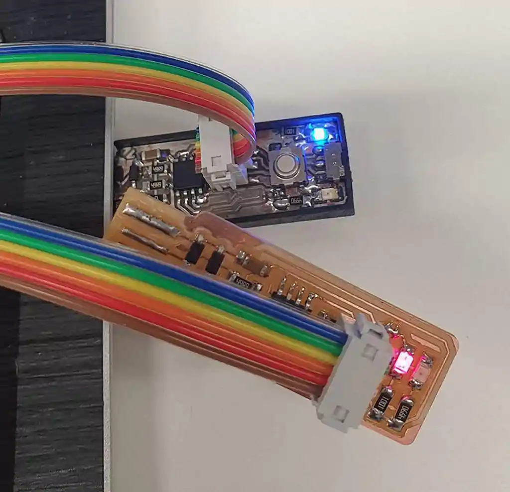
The FabTinyISP is plugged into another FabTinyISP for programming.The programming cable between was inspected for right polarity. The red indication led comes on when the cable is connected right.
First, the firmware is programmed by command.
make flash
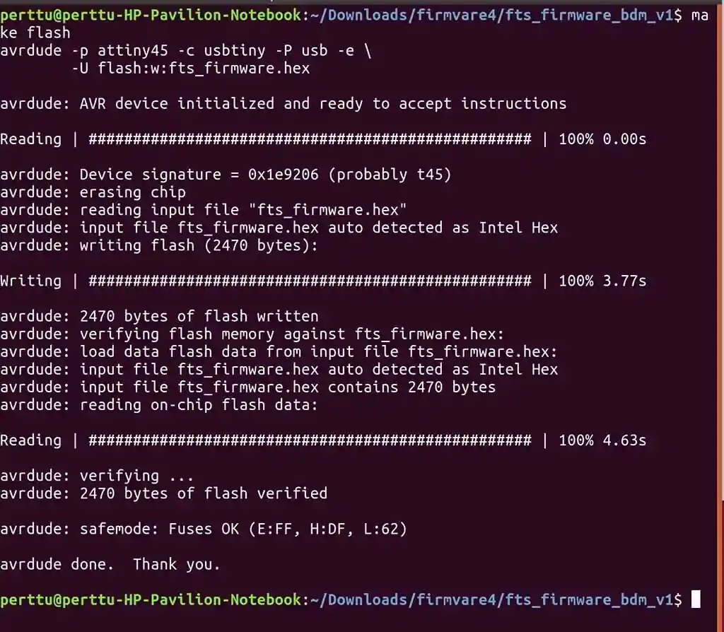
Then fuses are programmed with the command.
make fuses
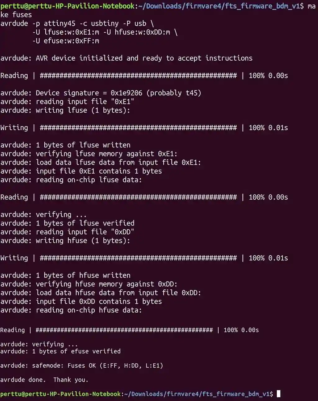
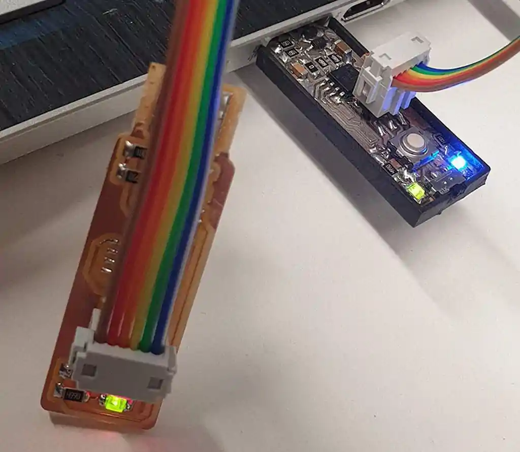
During programming, the green led can be seen light up from both FabTinyISP’s. It is a sign for something working.
Then the programmer is removed from the other programmer and inserted to the computer’s USB port. After executing lsusb you should read “Multiple Vendors USBtiny”.
Then the reset disable bit is set that the ATTiny45 cannot be reprogrammed anymore by accident. The board was tested by before the resetfuses command.
make rstdisbl
The solder jumper was removed using solder wick. The extra solder was also removed from the USB contacts.
3D printing case for the FabTinyUSB
I designed case for the FabTinyISP. I used Inventor 2019 for the design.
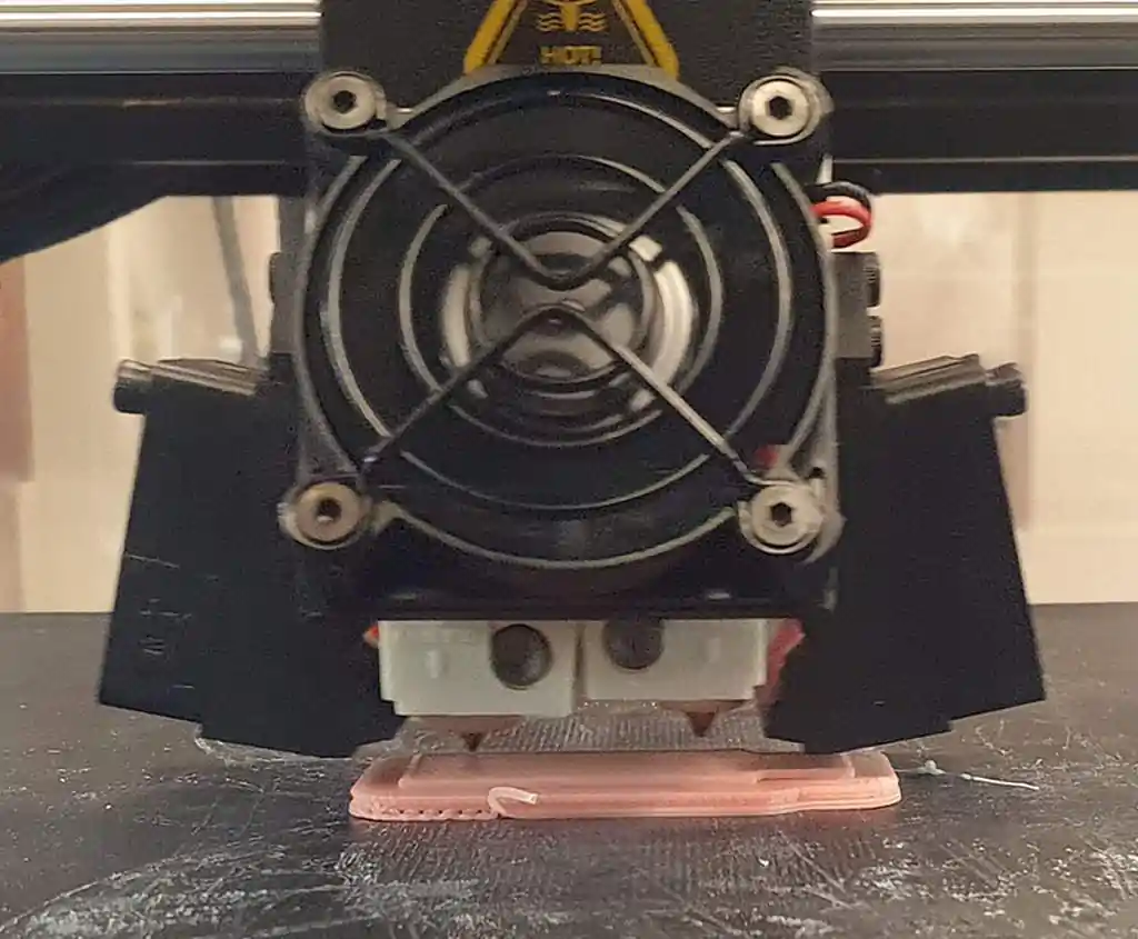
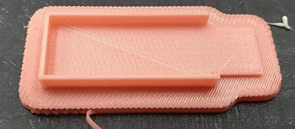
The finished support case on buildplate with raft.
The raft that helps with the buildplate adhesion and the straightness of the final part releases from the case easily by little bending.
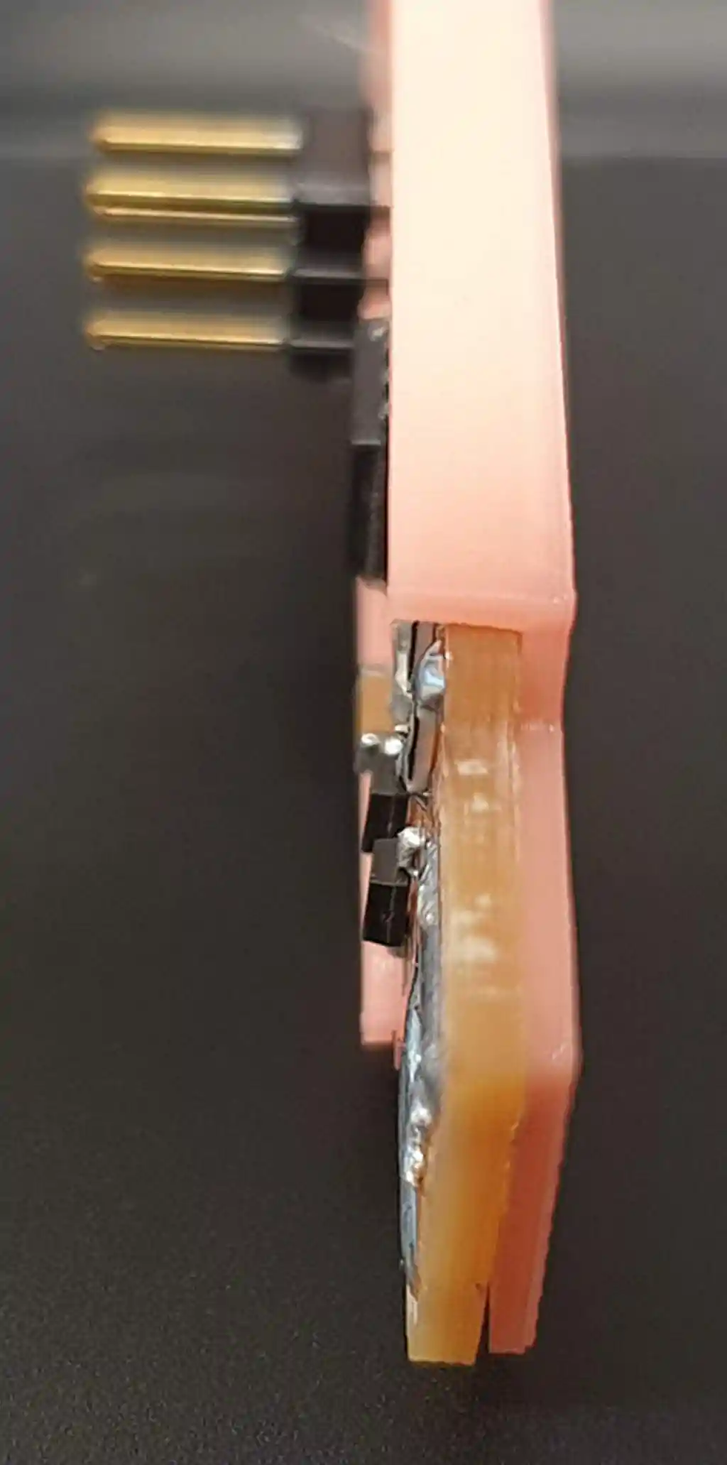
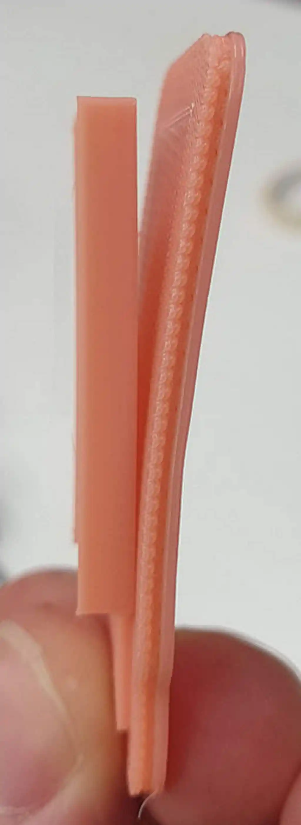
The 3D printed case fits nicely to the FabTinyISP. Press fit is enough. No glue is needed.
The finished product.
All used files can be found on my gitlab repository