Week 5: Electronics Production
Welcome in XXI century, those are words, which I'd like to start as reporting for work done in previous week. Design of electronics is really interesting process. Anyone could do it, even at home. For such you would need an iron, laser printer with some special paper sheets and of course your own design. Later on there is need for some weak acid, patience and soldering station. I used to do such stuff as a hobby during my studies in Gdansk.
Of course there are also totally professional approaches such as ordering PCB (Printed Circuit Board) from external company, which would take a bit of your money in exchange of their work. If you are careful with your documentation they may even solder your components onto PCB. Usually those companies are not affected by such limitations as your own 'home-brewed' technology of making PCB. Still you have to wait quite a long and costs are much higher.
I learned that third option is to use your FabLab premises. In Oulu we are able to use Roland SRM-20 Desktop Milling Machine. By using mill it will remove all unwanted copper from your plate and create electronic design. Copper is always placed on some insulator, the substrate would be same as one you could use at home - FR#, where # is a number explaining on what kind of material copper is placed, e.g. glass-reinforced epoxy laminate, which is fire resistant.

Group Assignment
The dreamteam remained untouched: Gleb, Marjo, Perttu and me
We should characterize the design rules of our machine. It means we should check how small traces we are able to mill. Milling is a process, where you are using small milling bit, which is going line by line and it removes some depth of material. I believe we could even create sculptures with such technique, let's say a pyramid. First of all we should consider our mill sizes, as those are influencing the final result most. We will use copper plates for cutting out our electric design, obviously copper is quite decent conductor. Material below is isolator, we can create logic and traces to connect our components so they are able to do something.
Spoiler alert: We are preparing to build programmer for future usage. It will allow to program (teach) our microcontrollers in the future. We will use ISP for programming.
It is important to choose drill properly. Those are mechanical parts and are breaking really easy. Friction is main physical phenomenon in milling. Even that steel is much harder than copper and plastic, drills are getting weaker and weaker. Approximately, one PCB costs around 0.1 $ (10 cents), which is really good price - comparing ratio of price to accuracy.
If drill has to be changed VPanel is handy (please check figure related to it, just below). In order to do detach the drill View button has to be clicked . It will move the drill to most reachable position (as high as possible, on the front).
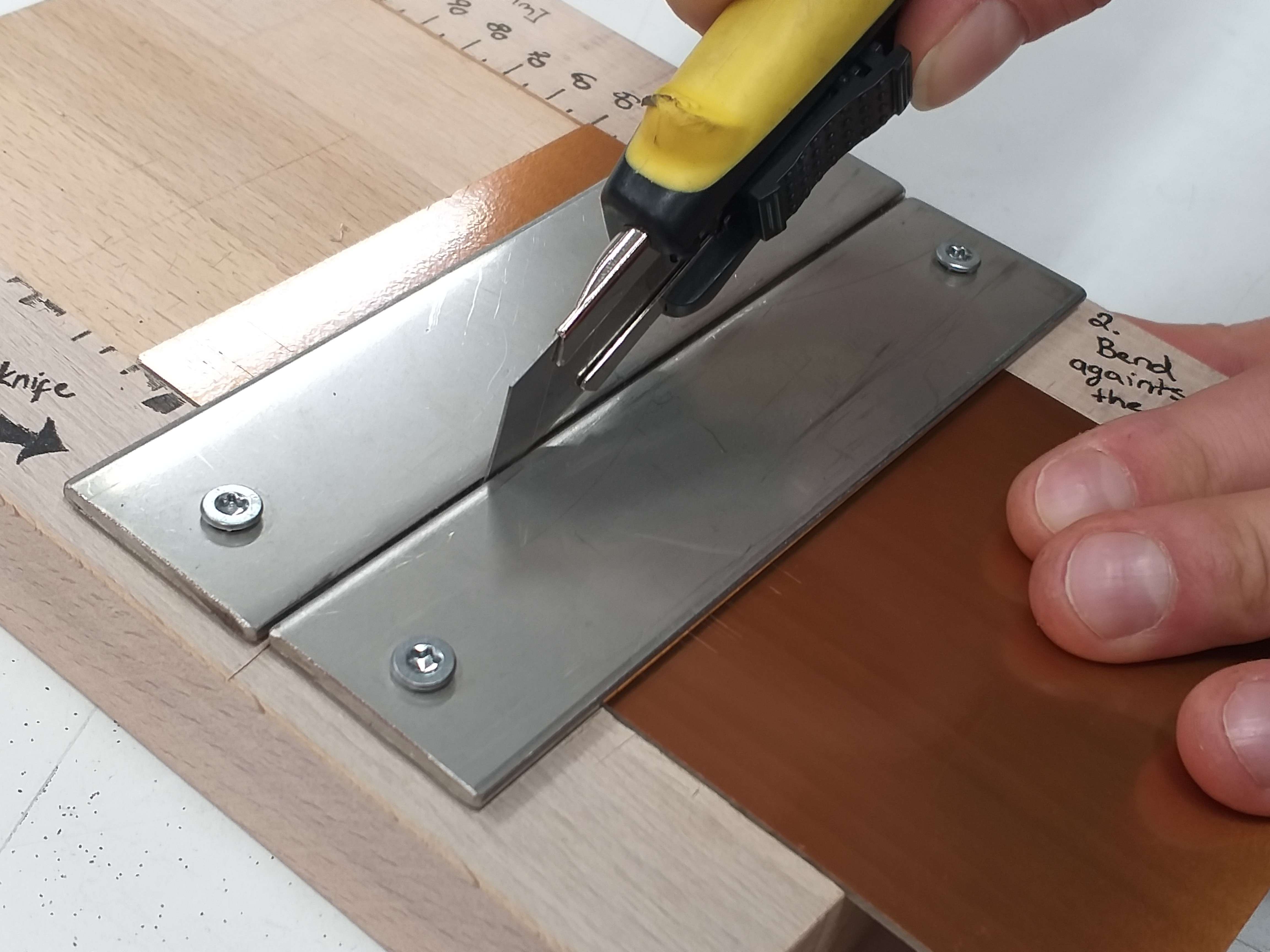
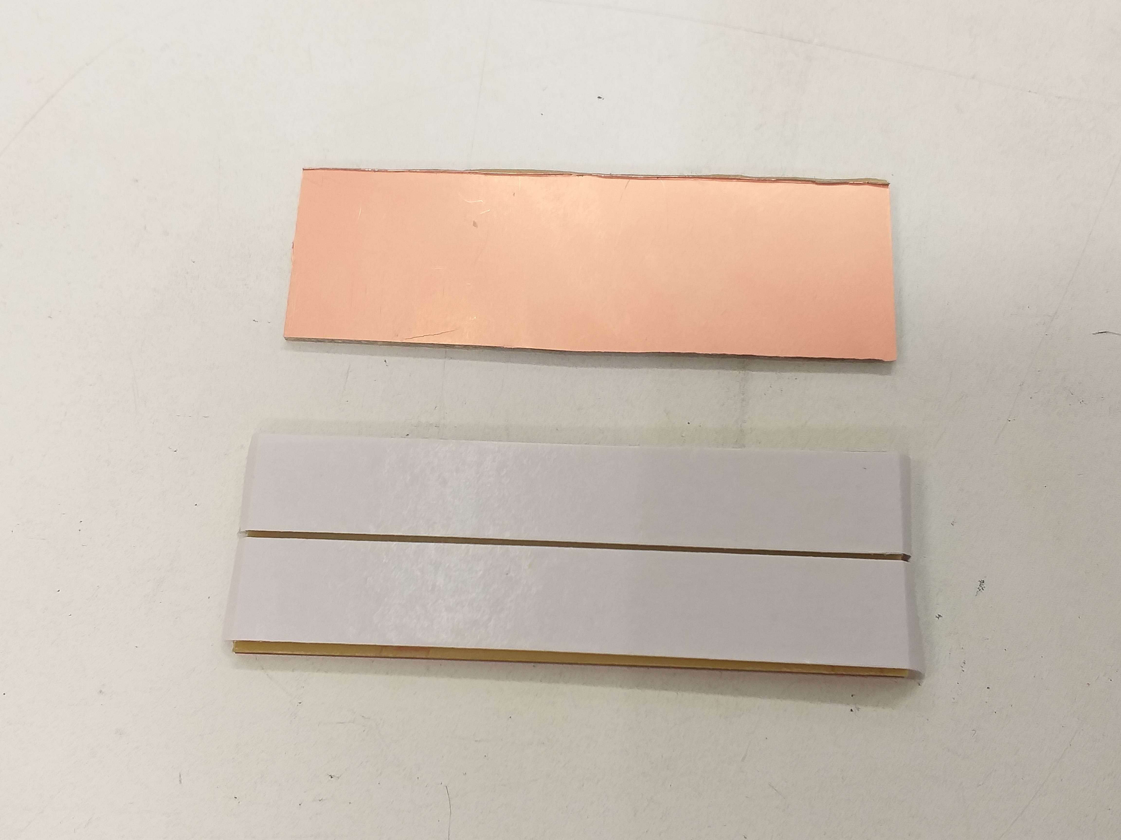
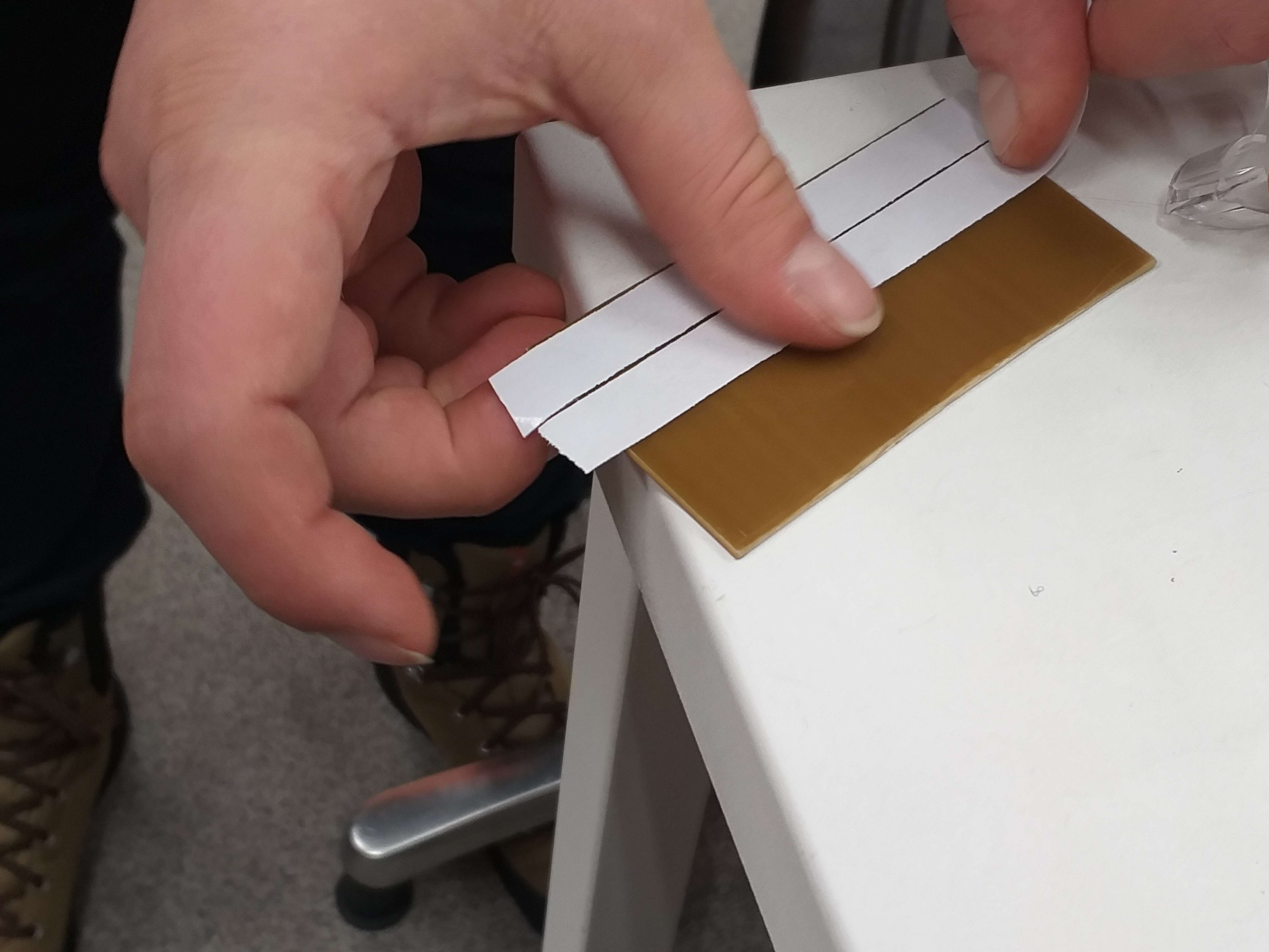
Our board should be cut from a bigger plate first. As it is shown on the image below. We should also ensure the surface is flat. In case of any differences in thickness the milling bit won't go evenly and there might be issues with short circuits. After that bottom part of the plate should be carefully taped (no overlapping lines of tape). After that we can carefully attach the milling bit inside of the machine.
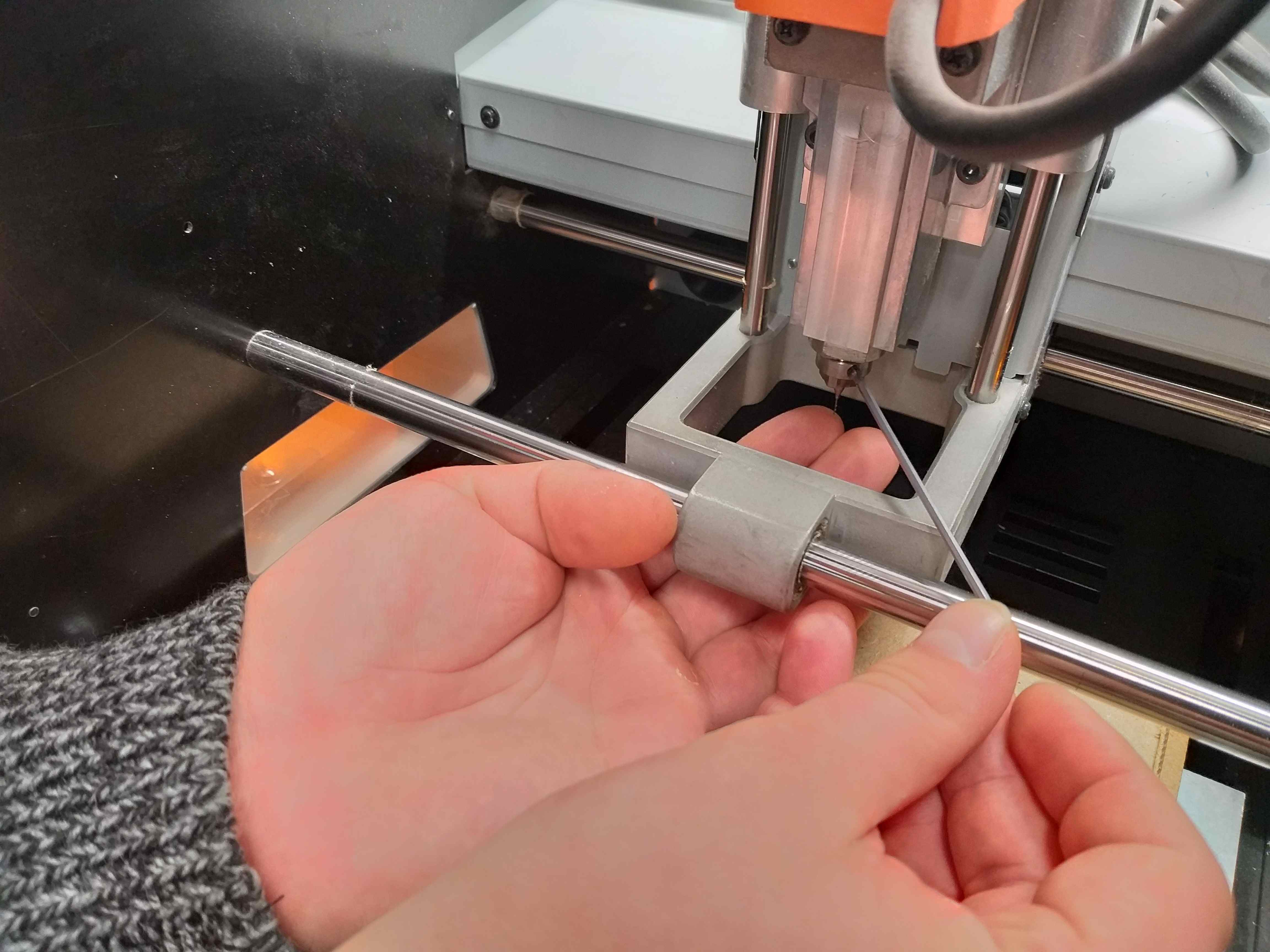
Attachment of the drill is quite important procedure. First head should be moved to some accessible position. Drill has to be attached using screwdriver. Then head should be placed down as close possible along Z-axis. Finally milling bit could be released and adjusted to slightly touch the surface and re-tightened again.
Alright, at this point all mechanical parts are adjusted. What is left is playing with the software and setting correctly all values. Below, there is screenshot from the Roland dedicated software (VPanel). First of all it is necessary to position the drill over the substrate.
The beginning position can be adjusted with X/Y and Z buttons marked with red rectangle. X - is moving the table, where Y and Z are in charge for moving the head. Just below increment step might be found. This is extremely important when playing with Z- axis as this requires highest precision. Continue step must not be used with Z axis! This will most likely break the milling bit if motion will continue inside of the material! Just after finding right position in X/Y/Z plane reset the position by pressing corresponding buttons (marked by green rectangle).
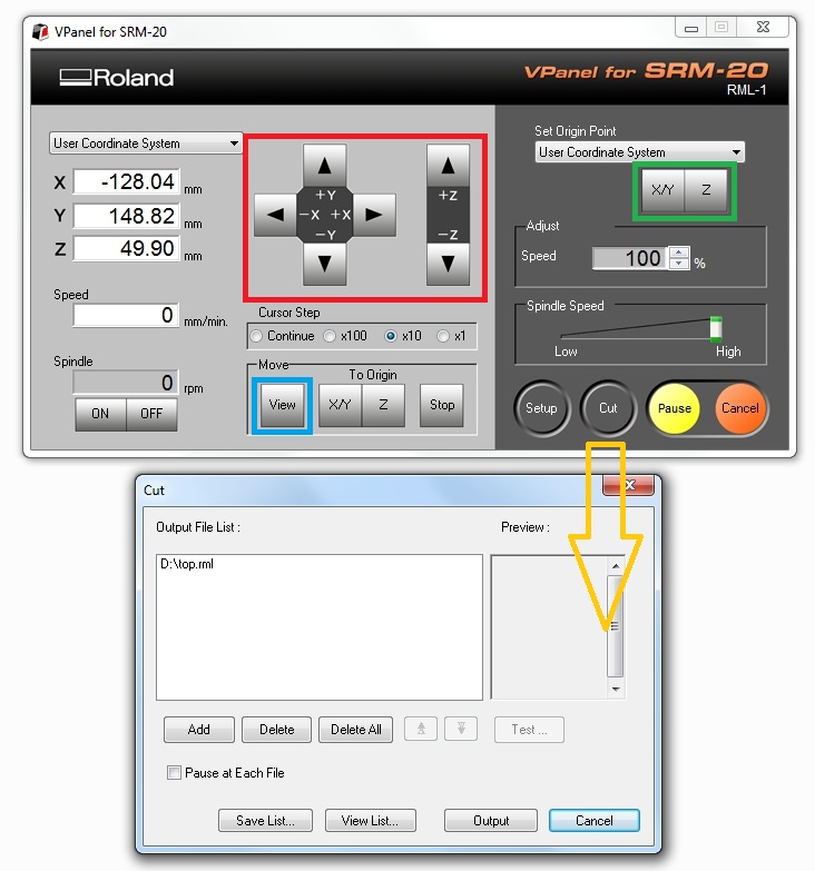
When everything is positioned and reseted correctly it is time to press cut button, marked with orange arrow. This will bring window, where desired file might be loaded. By clicking Add successive files should be added. Mistakes can be corrected with Delete button. In the end Save List has to be clicked. There could be multiple boards cut at the same time (Nevertheless, we did not use this feature). Very handy! Process should be started by clicking "Output"
Simplified procedure of fabrication/milling process of PCBs:
- Choose proper milling bit
- Find substrate
- Cut a piece with size of your board (you can check it in design Software)
- At this point I assume PCB is saved as RML
- Carefully attach drill
- Position your drill in XY-axes and set begin point
- Using VPanel set position of milling bit in Z-axis (as close to the surface as possible)
- When you are close to the surface you may unscrew milling bit and let it touch the surface, then lift it using VPanel for circa 0.5 [mm]
- Load the RML file and start milling
- Position outline and choose proper settings for milling outlines
- Move the head to comfortable position and change milling bit
- Start milling
- Remove the shavings
- Clean your board with alcohol, Isopropanol will do
- Take it off, it is ready for soldering
Limitations
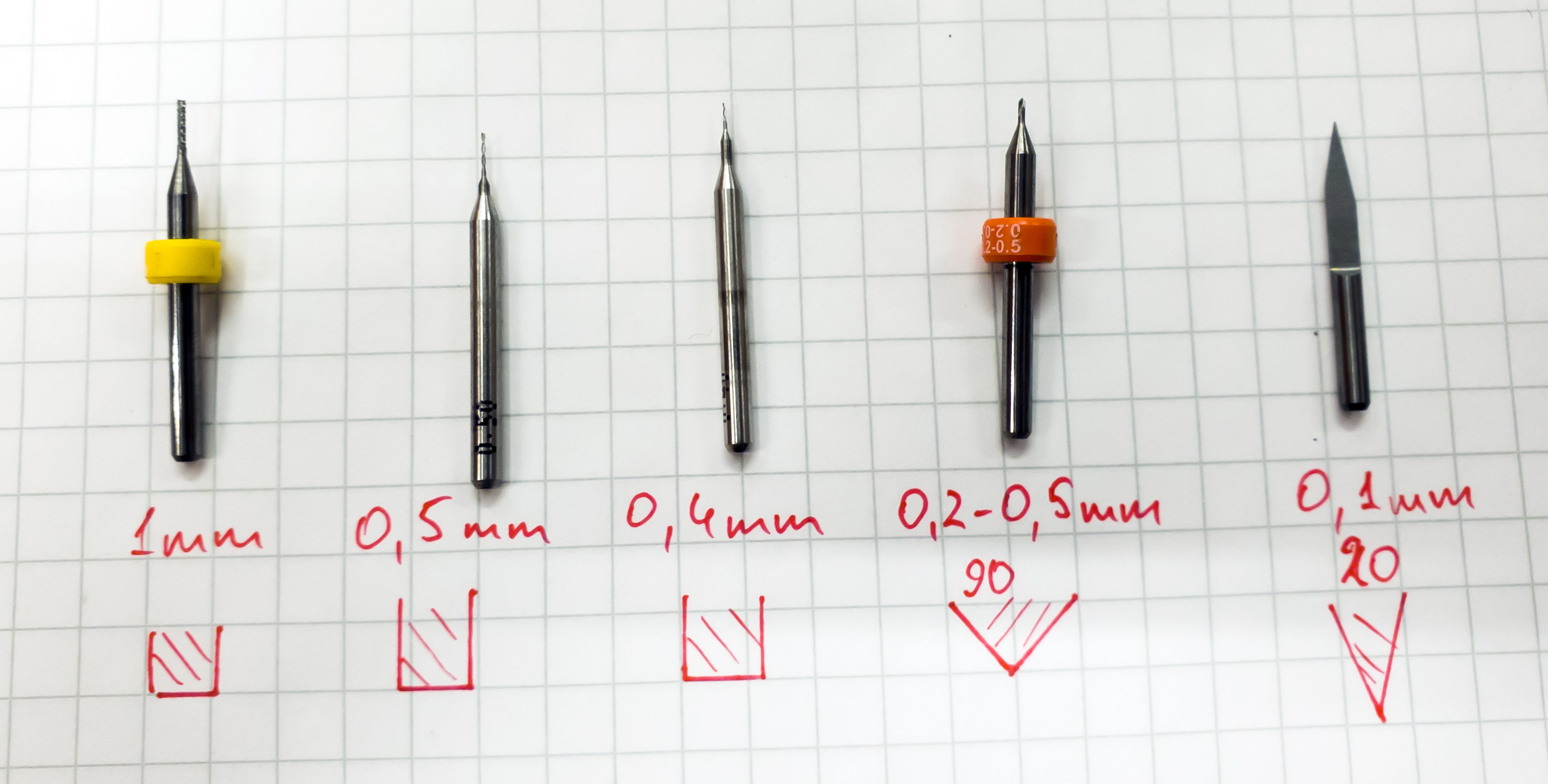
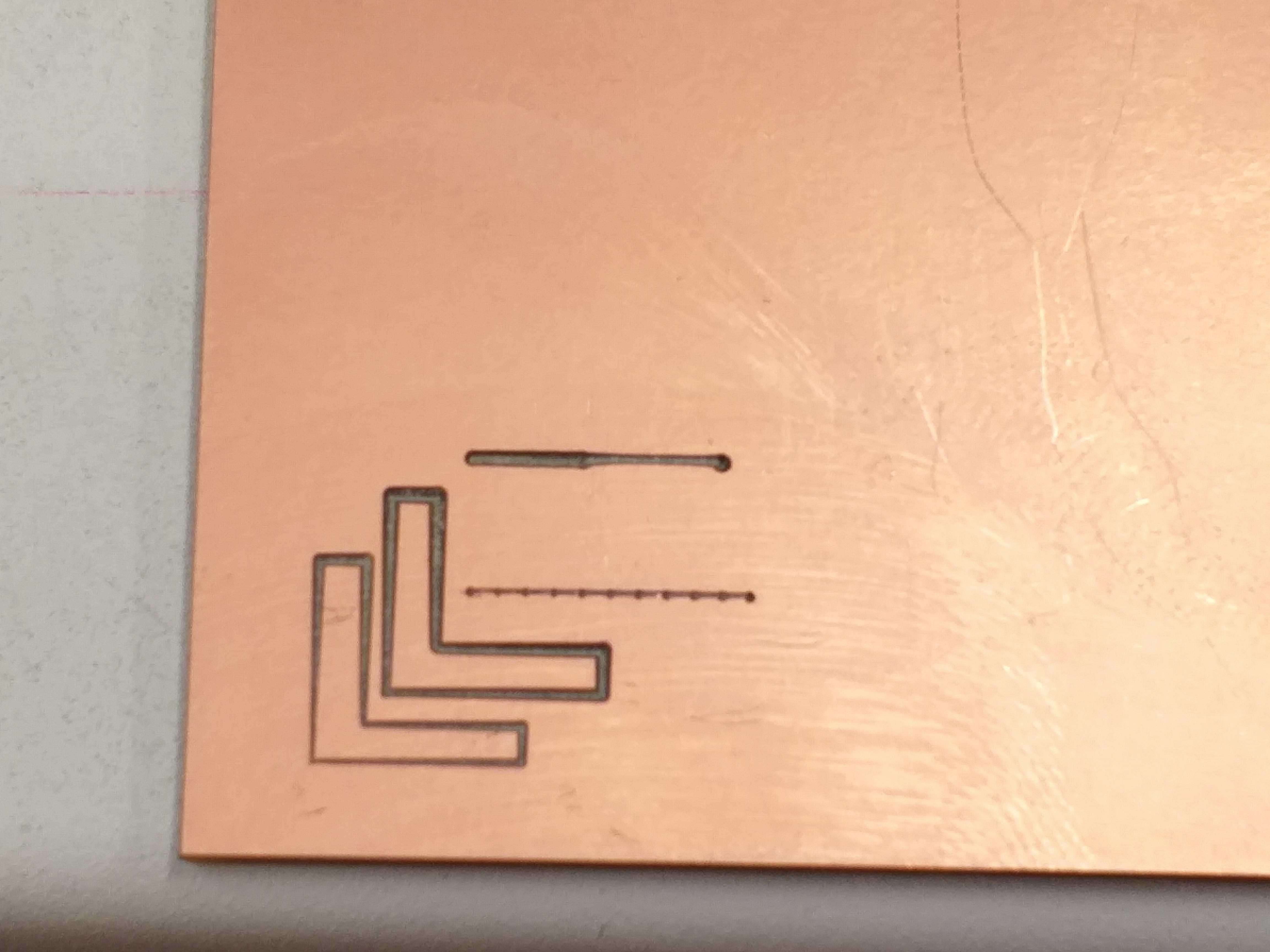
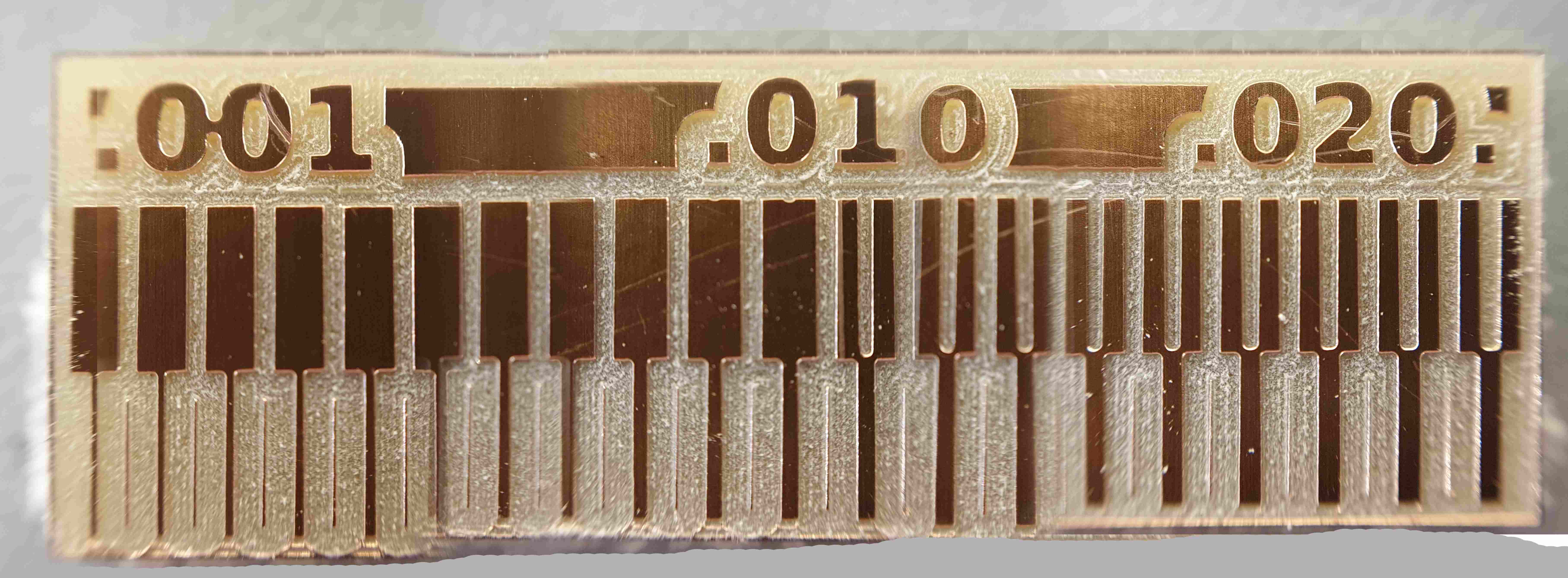
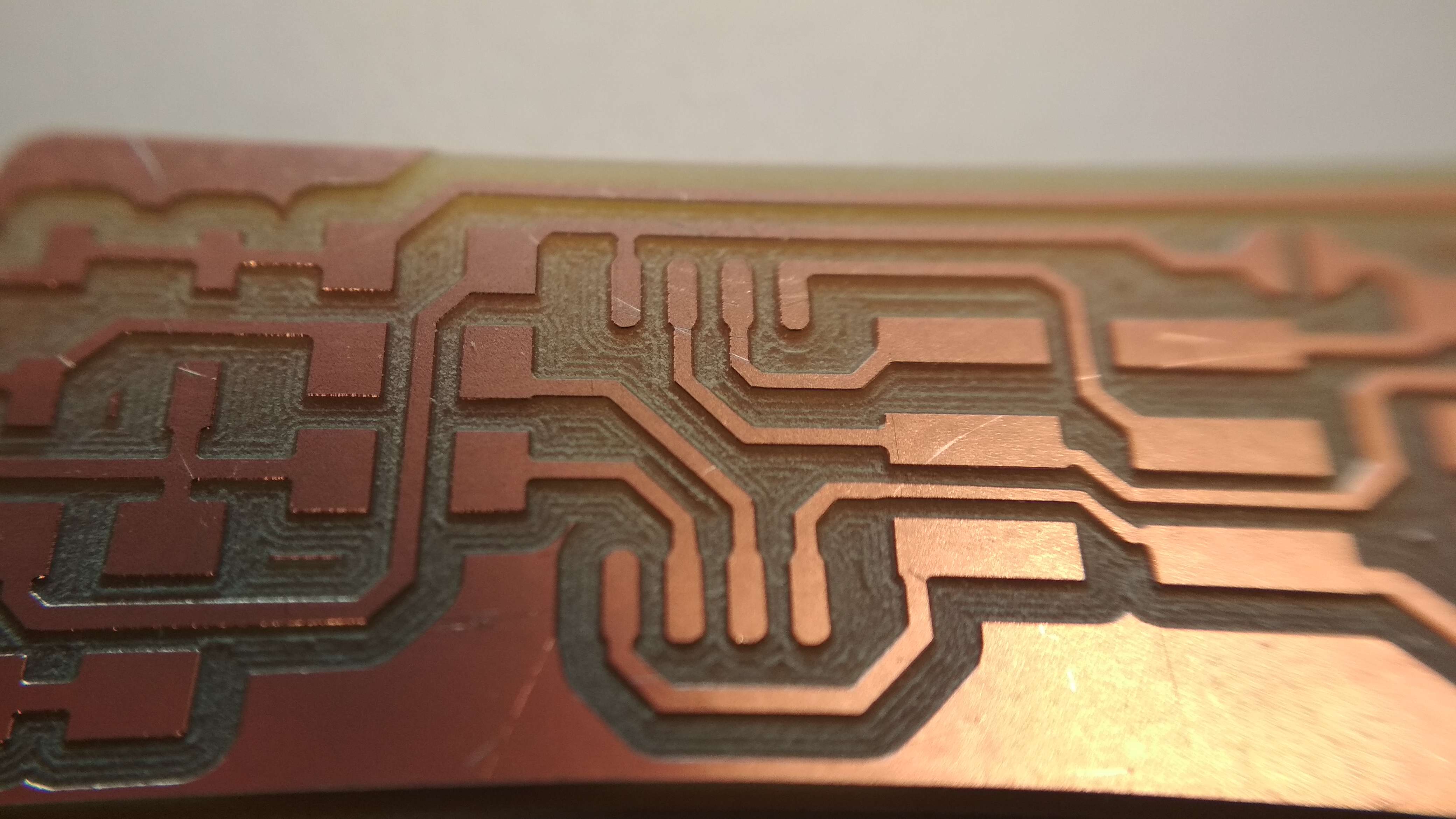
So far no problems occurred. However, there must be something, which is stopping us from creating ultra-small circuits. Something, which prevents from unbelievably precise PCBs. Unfortunately there is couple things. First of all drill size is somewhat limiting us in the milling. Second case is step of motors, this is also not finite and have some strict values. Nevertheless it is usually smaller than used drill and third factor. Even that we are using really small drill sizes, when drill routes are close to each other they will rip copper from the surface. Leaving nothing but an empty hole. We created a test drill to estimate couple constants
Drill_1: 0.2 - 0.05 [mm] 90 degree milling tip
- How close traces may be placed - size of drill head
- What is minimal width of a trace - 0.025 mm
- What is ability to drill between traces - till 0.25 mm
| Result | Drill | Sizes |
|---|---|---|
 |
 |
triangle |
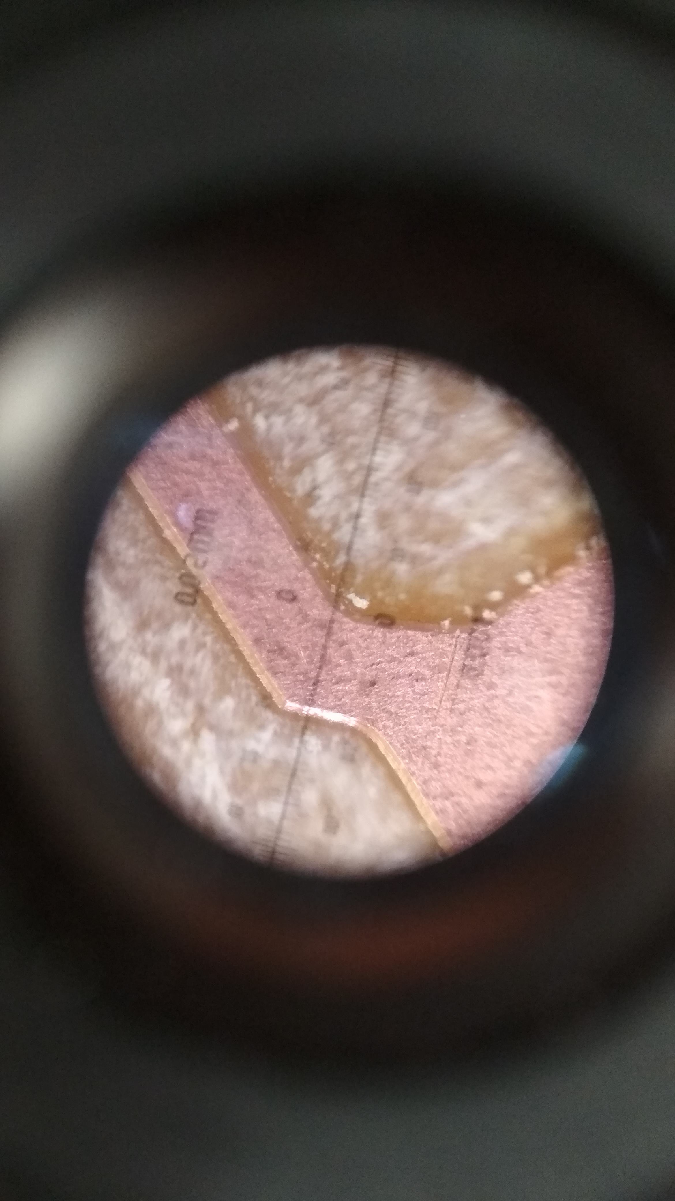
Drill_2: 0.4 [mm] flat milling tip
- How close traces may be placed - size of drill head
- What is minimal width of a trace - 0.18 mm
- What is ability to drill inside of a trace - till 0.457 mm
| Result | Drill | Sizes |
|---|---|---|
 |
 |
flat |
Individual Assignment
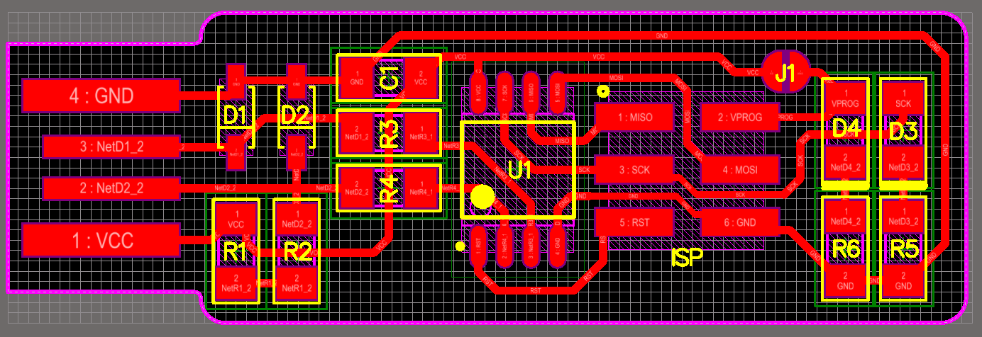
Using Brian's files and a bit of work in MOD's it was possible to cutting traces (.RML) of programmer circuit (procedure below). Using previously gained knowledge I cut it out using milling machine. It did not take a long time.
- Go to MODs
- Go to: programs/open server program/SRM-20(PCB)
- Delete WebSocket Serial module
- Create Save file module (right click): modules/open server module/file (save)
- Read your PNG file: Press select
- For milling traces choose: mill traces 1/64 for outlines mill outline 1/32
- Set origin coordinates (x, y, z) to (0, 0, 0)
- Set milling bit size (in my case it was 0.4 mm)
- Note: for milling outline different milling bit should be used, e.g. 1 mm
- Connect output Roland SRM-20 milling machine to Save file
- Define tool diameter and cut depth in mill raster 2D module
- Mill raster 2D module press: calculate
- Save the file
- Optionally it is possible to see the RML file by clicking view
In order to prepare for milling the outline, second file has to be opened. and similar procedure need to be followed. Cut depth is already defined, no need to play with this value, only if you are using non standard PCBs. After going trough both files there is a bit of work with VPanel, there is usually need to change the drill between milling the board and outline. How to properly use VPanel was described in the group work.
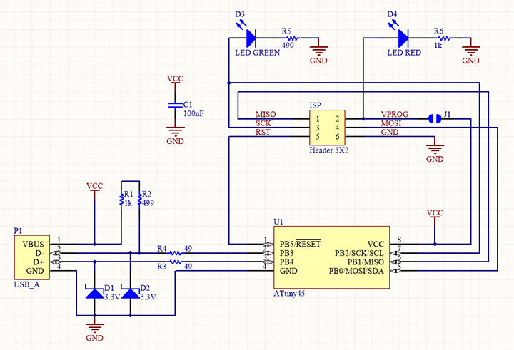
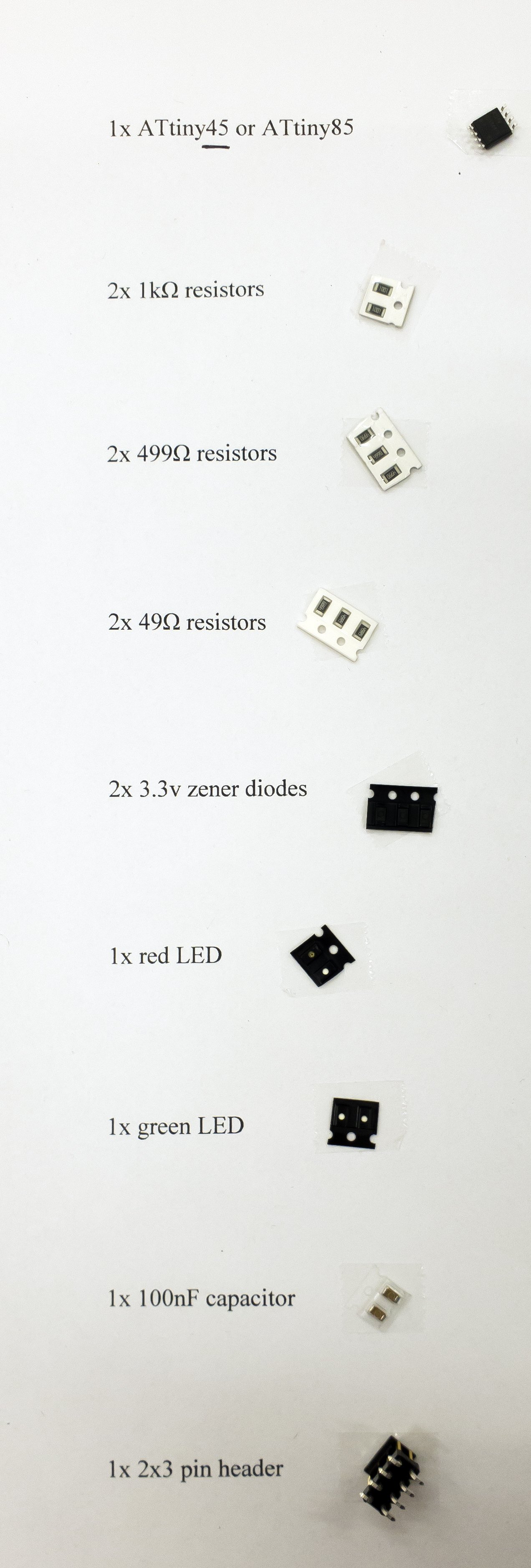
The next step is preparation of electronic components. Once again using Brian's web page I managed to find Bill of materialsand localize corresponding parts.
What is left to do is soldering. This is how soldering surrounding looks like. There is a lot of available tools beside most obvious - soldering station. Except of must-have machines such as sort of fume extractor to get rid of soldering gases and copper braid to remove short circuits there are other handy tools. An example tin sucking tube, hot air gun.

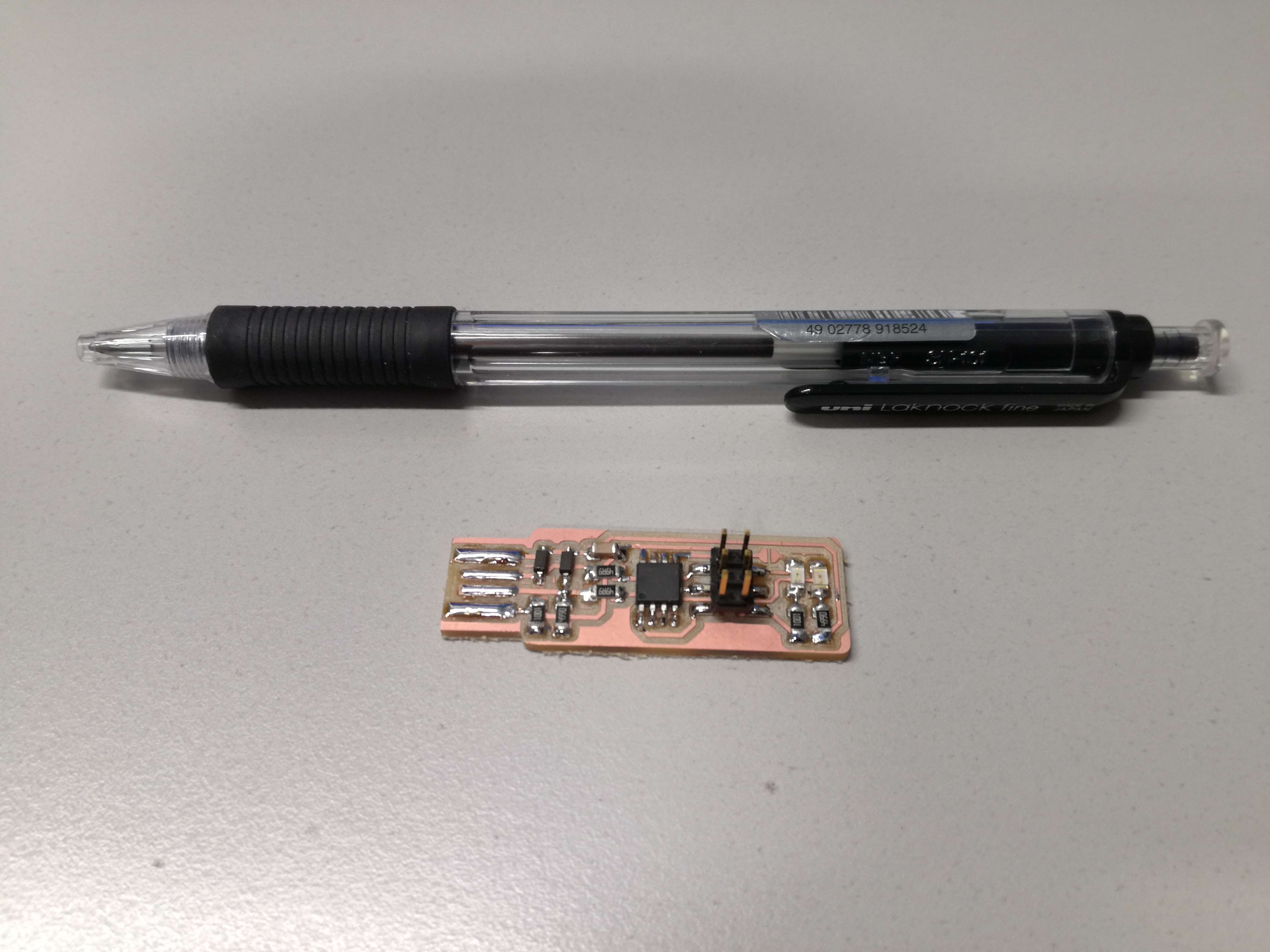
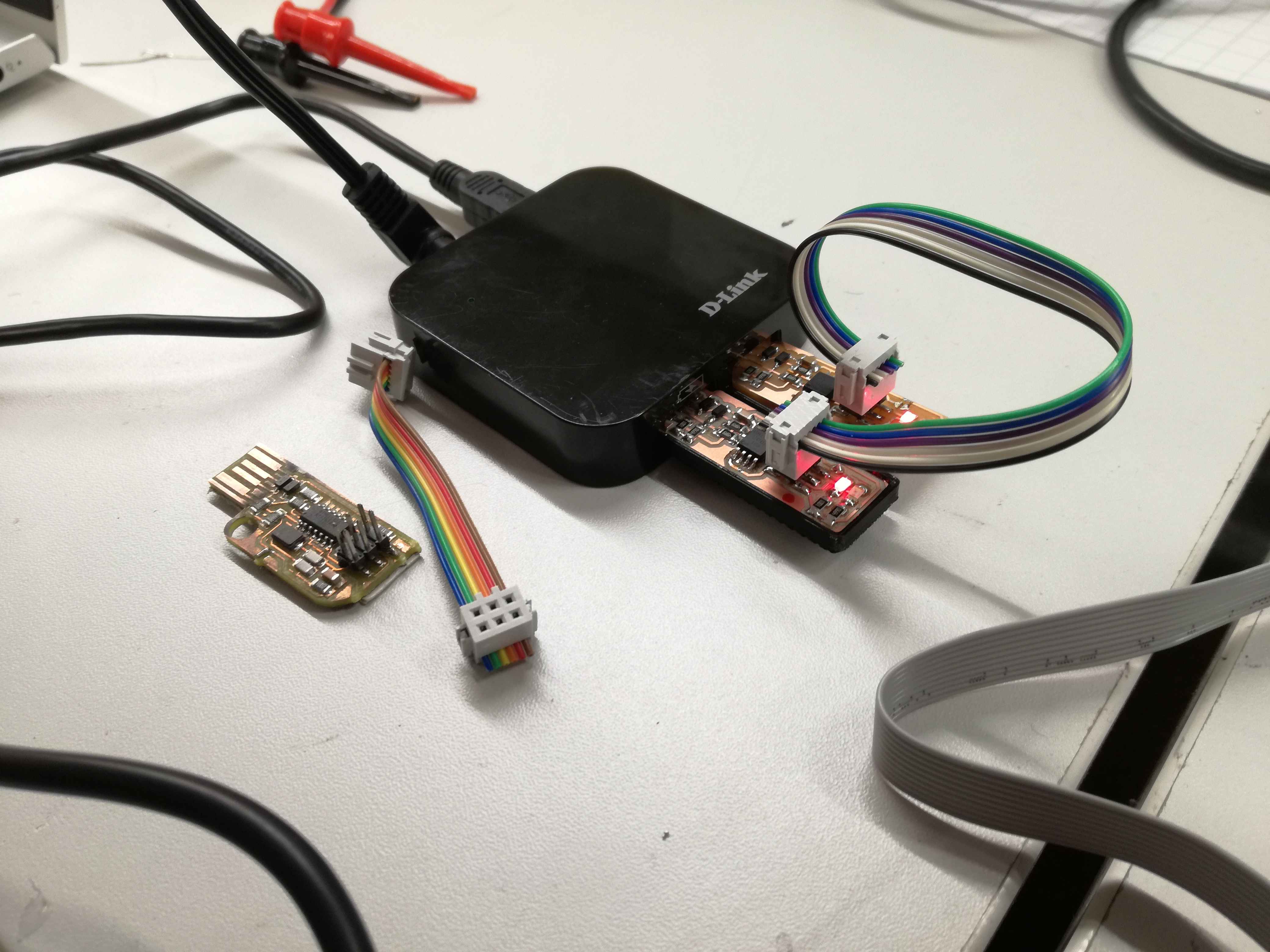
Final PCB is shown below. It is a good approach to clean it after soldering as there are drops of flux. Of course standard right now is lead free tin. This affect the temperature, in which tin is melting. In my case I was using 370 Celsius degrees, which is quite standard in my eyes. In case of bigger copper areas temperature might be adjusted. In case of soldering thick wires to big ground areas even 400 degrees for very short time.
Programming a programmer
There is one last step before my programmer will become functional tool. I need to flash it and load software onto it (The snake is eating it's own tail).
However, there is one important thing before programming. Testing connections with multimeter and ensuring no shorts. In my case there were no short circuits and everything was connected (no missing traces, etc).
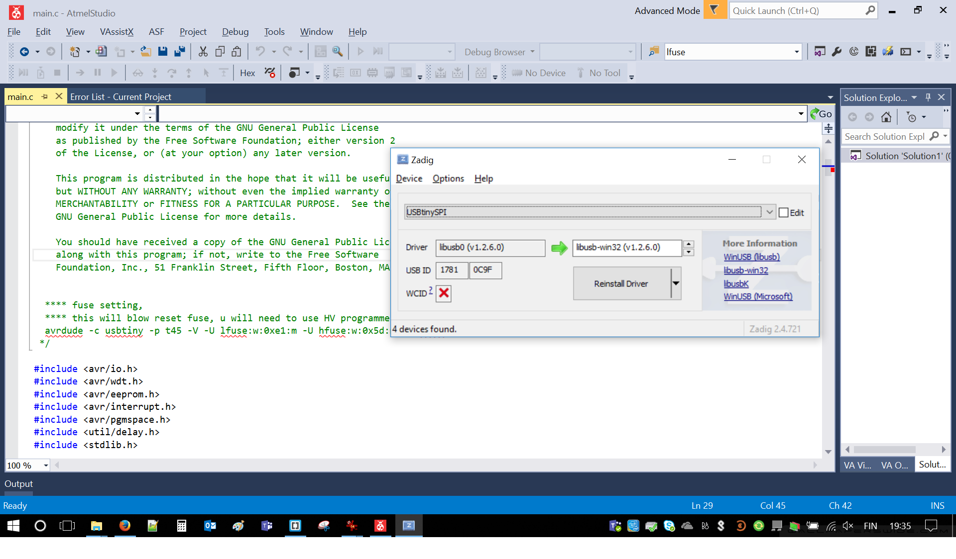
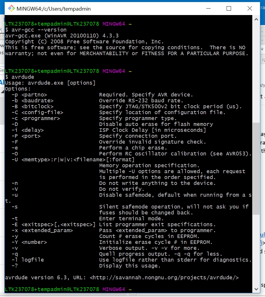
Thanks to Alok, I could use his programmer and workstation. There was quite many attempts , in which we used following software:Avrdude, Atmel studio, Zadig. I tried both available programmers: Alok's FabUSBtiny and USBasp.
Fortunately, I managed to make my programmer functional.
Everything started with Zadig, it is a software used to install the drivers. Without those, Windows is unable to recognize what kind of device is connected. Below, there is proper way to set Zadig (driver and device).
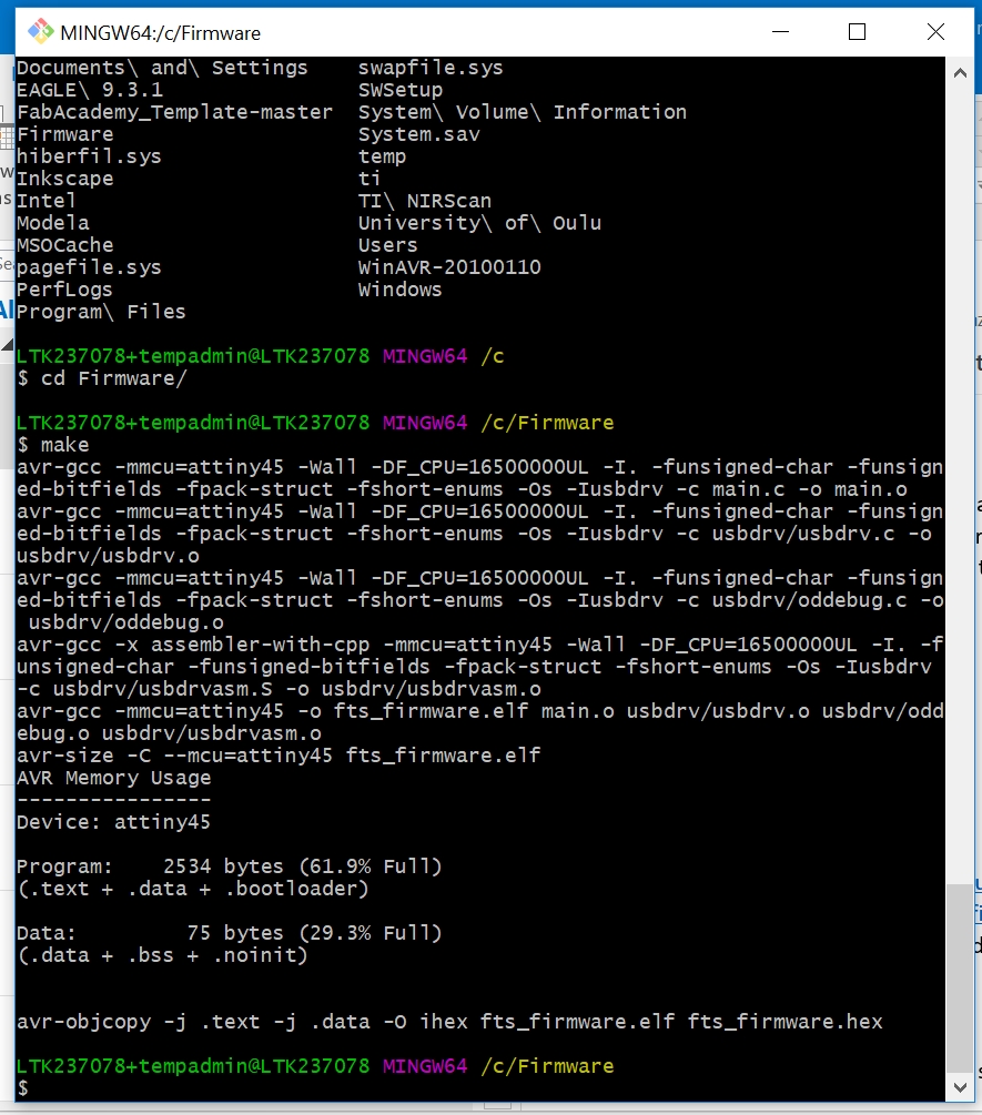
After making file with avr-gcc. I decided to use command window for programming purposes.Firstly I injected or flashed firmware onto the chip, results below. It required following code:
avrdude.exe -p attiny45 -P usb -c usbtiny -e -U flash:w:fts_firmware.hex
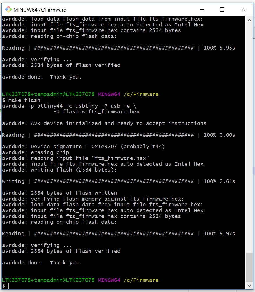
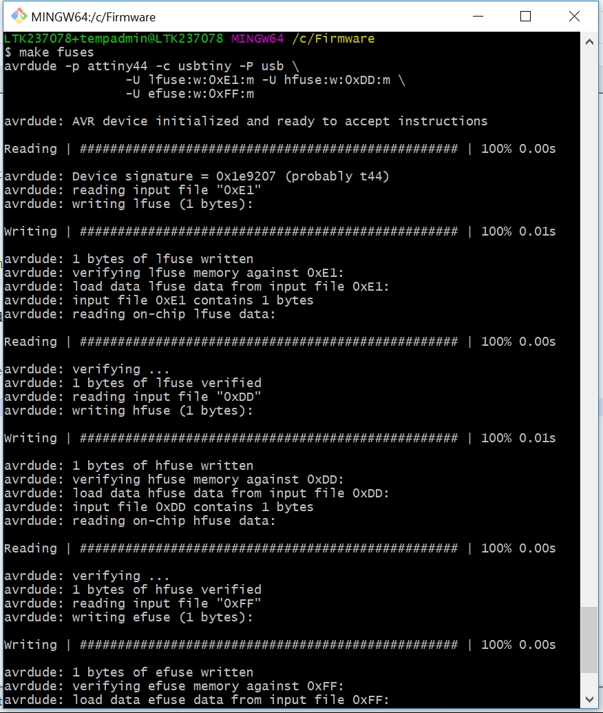
In next step, I simply flashed the fuses. This step looked very similar to previous one. This time I used following command:
avrdude.exe -p attiny45 -P usb -c usbtiny -U lfuse:w:0xe1:m -U hfuse:w:0xdd:m -U efuse:w:0xff:m
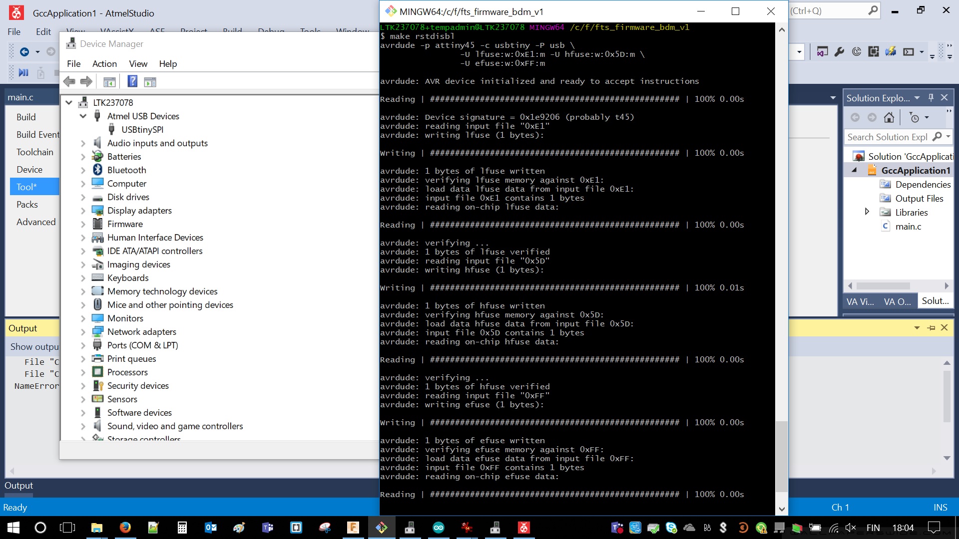
Final step was point of no return. After utilizing below code my USBtiny programmer could not be reprogrammed without using HV programmer.
avrdude.exe -p attiny45 -P usb -c usbtiny -U lfuse:w:0xe1:m -U hfuse:w:0x5d:m -U efuse:w:0xff:m
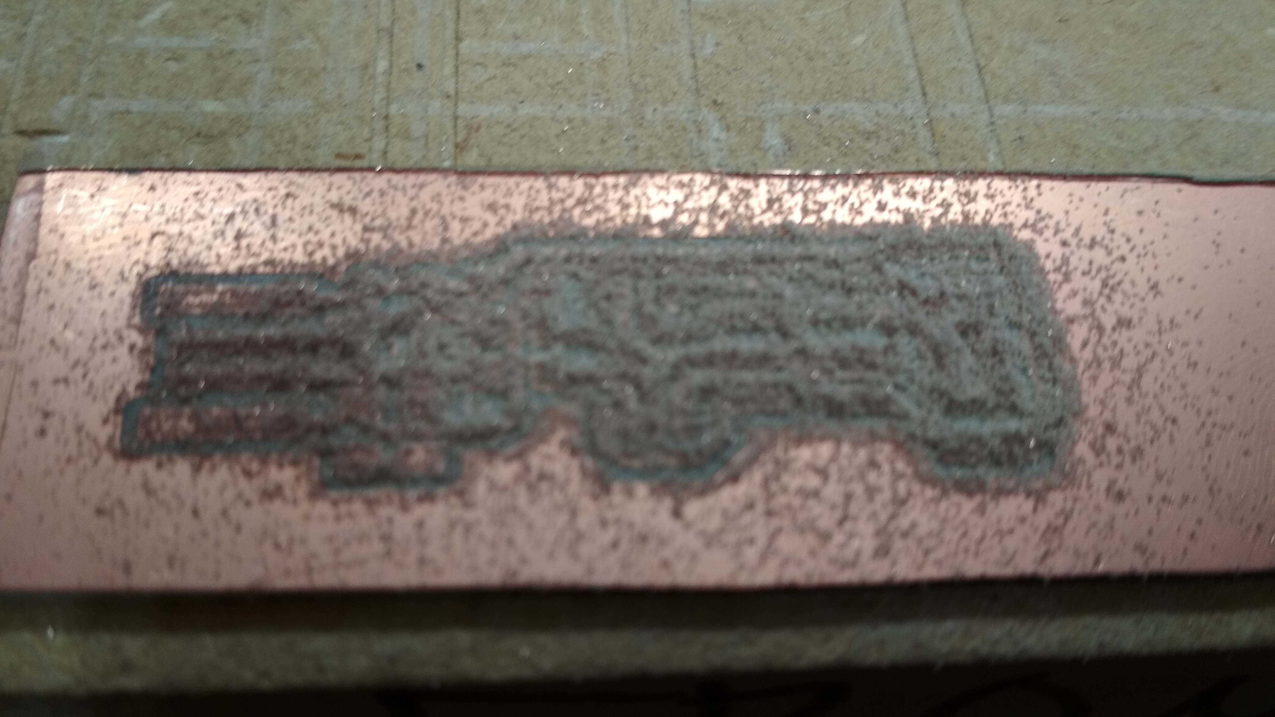
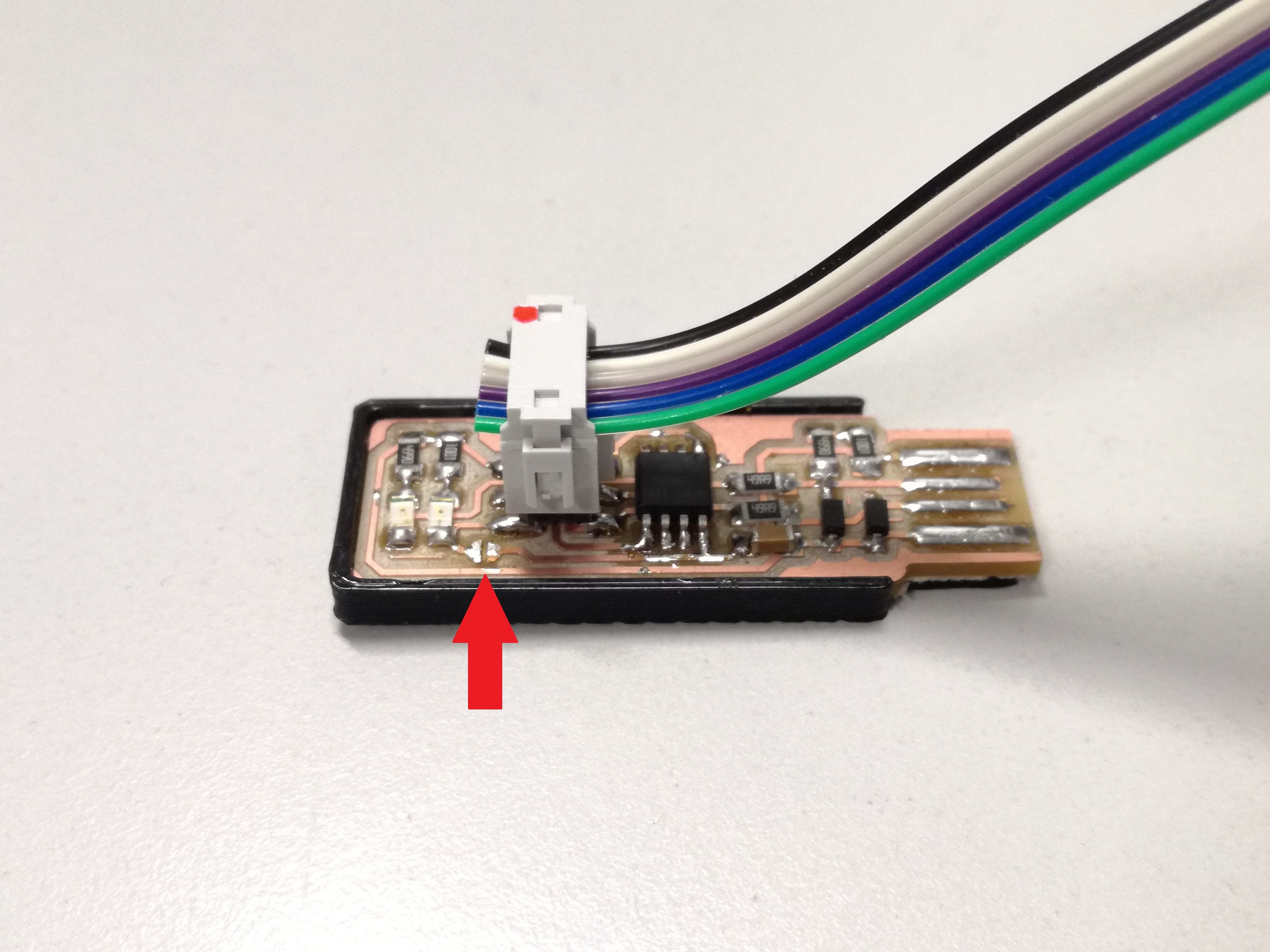
Process was fairly simple and quick. The very last operation to perform was removing bridge made with tin from the PCB. I used copper braid for that
Assignment was a success. Here a little photo (known as hero shot) of fully functional programmer. I highlighted place of ex-bridge.
Files:
Download: Atmel studio programming filesDownload: Programmer traces
Download: Programmer outline
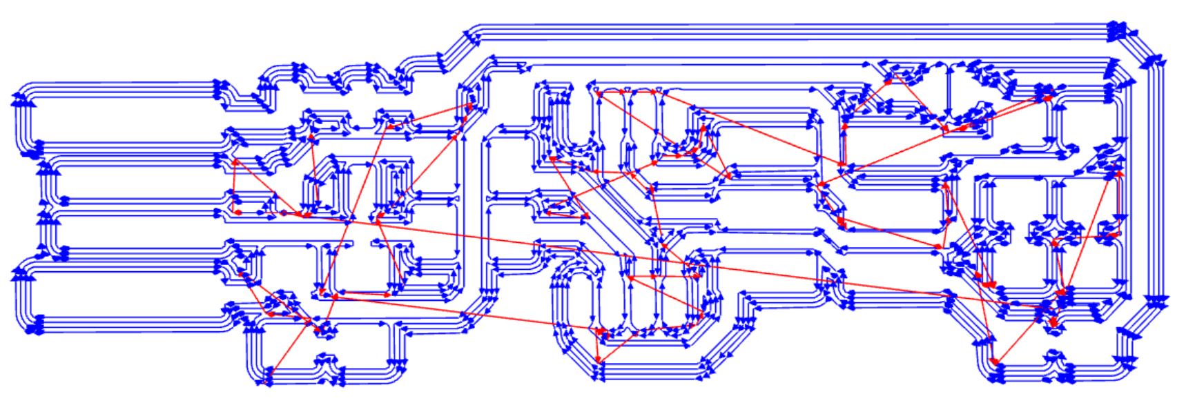
Download: Group Work traces
Download: Group Work outline